Strain-gradient mapping of semiconductor quantum dots
In the context of fast developing quantum technologies, locating single quantum objects embedded in solid or fluid environment while keeping their properties unchanged is a crucial requirement as well as a challenge to engineer their mutual interaction. Such “quantum microscopes” have been demonstrated already for NV-centers embedded in diamond Rittweger , and for single atoms within an ultracold gas Bakr . In this work, we demonstrate a new method to determine non-destructively the position of randomly distributed semiconductor quantum dots (QDs) deeply embedded in a solid photonic waveguide. By setting the wire in an oscillating motion, we generate large stress gradients across the QDs plane. We then exploit the fact that the QDs emission frequency is highly sensitive to the local material stress Trotta ; Yeo ; Montinaro to infer their positions with an accuracy ranging from nm down to nm.
Due to their atomic-like properties, semiconductor quantum dots have been widely used for solid-state cavity-quantum electrodynamics Gerard ; Lodahl , and display attractive applications in the field of quantum photonics as a key building block to realize bright quantum-light sources Claudon ; Dousse ; Munsch ; Ding and spin-photon interfaces Besombes ; Awschalom ; DeGreve ; Gao . To date, high-quality QDs are mainly obtained via a self-assembly process, which produces nano-islands that are randomly distributed in a plane. An accurate, non-destructive mapping of the QD position is thus a key capability in the general context of quantum nanophotonics. The precise location of a QD within a photonic nanostructure indeed determines the strength of light-matter coupling. The relative position of distinct QDs is also crucial to investigate their mutual coupling Wieck_2005 ; Kasprzak ; Savona_2005 ; Mermillod and collective effects such as superradiance Temnov ; Auffeves . Although impressive results have already been obtained by all-optical imaging methods Betzig_NSOM2 ; Rittweger ; Matsuda , they are not well suited for imaging quantum dots deeply embedded in photonic nanostructures.
In this work, we propose and demonstrate a non-destructive QD mapping technique whose principle is reminiscent of Magnetic Resonance Imaging (MRI) Brown ; Mamin ; Degen . By setting the structure in which the QDs are embedded into vibration, we generate across the QD plane an oscillating stress field with a large spatial gradient. The QD emission energies then display a spatially-dependent oscillation, whose amplitudes and phases are resolved by stroboscopic microphotoluminescence. By using two cross-polarized mechanical modes, we perform a 2D mapping of the QD position in the growth plane. As opposed to optical near-field techniques, this method can be used to determine the position of QDs that are deeply embedded within a solid-state microstructure, with a spatial resolution which is not bound by the laws of electromagnetism.
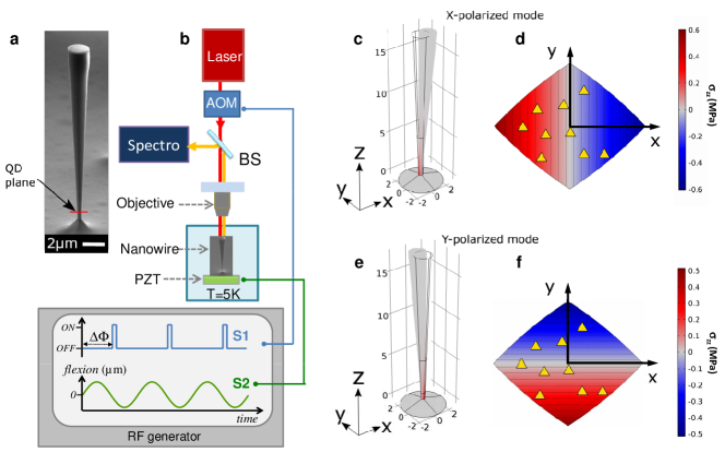
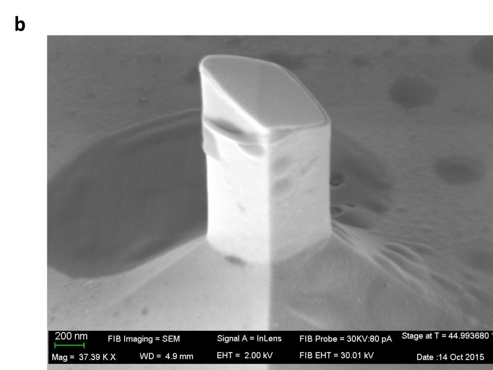
We demonstrate this technique on a tapered GaAs photonic wire antenna which embeds a single layer of InAs quantum dots (Fig.1.a). Similar photonic structures have been used recently to realize bright sources of single-photon Munsch , and hybrid opto-mechanical systems Yeo . The QDs are randomly distributed in a plane perpendicular to the wire axis, and located m above the structure base.
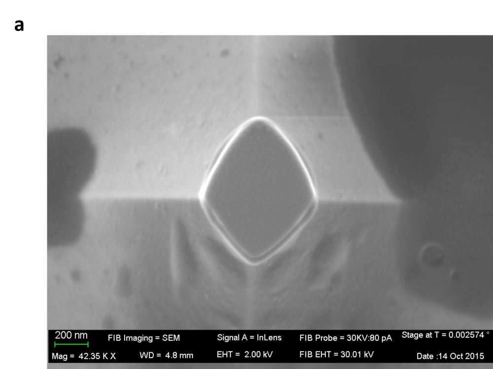
Mechanical spectroscopy of the wire vibration modes is conducted in vacuum, at cryogenic temperature (K). The wire is set into motion by a piezoelectrical transducer (PZT) attached to the back side of the sample. To perform mechanical spectroscopy, one sweeps the piezo drive frequency, while monitoring the top facet lateral displacement with an auxiliary laser and a split photodiode (SPD) Sanii ; Yeo ; Gloppe . We focus on the fundamental vibration mode, which corresponds to a flexion of the wire with a single node at its basis. Mechanical spectroscopy reveals here two low energy modes X and Y with eigen frequencies and , and a similar quality factor . The mode X (Y) corresponds to a vibration along the () axis in the laboratory frame. The observed mode splitting can be traced back to a lozenge shaped cross section of the wire base, with the longest diagonal aligned with the axis. We characterized this shape in detail by focused ion beam (FIB) milling and scanning electronic microscope (SEM) observation as illustrated in Fig.1.e (see SI, section A for details). These nanomechanical measurements are in quantitative agreement with a numerical finite element method (FEM) simulation, which involves a realistic description of the structure geometry.
In the context of QD location measurement, the splitting between modes X and Y is a precious resource: by simply tuning the excitation PZT frequency, one sets the orientation of the stress field gradient in the QD plane along the or direction. This feature is illustrated in Fig. 1d,f, which show the calculated maps of , the dominant component of the stress tensor, for the two vibration modes. Moreover, the conical wire shape leads to very large stress gradient amplitudes: for a lateral displacement of the nanowire top facet, the stress gradient typically amounts to . Like in MRI, a large gradient is a crucial asset to obtain a strongly space-dependent QD response. FEM simulations also show that the gradient is constant to better than in the QD layer. Although not mandatory to enable strain-mapping, such uniformity greatly simplifies the data analysis.
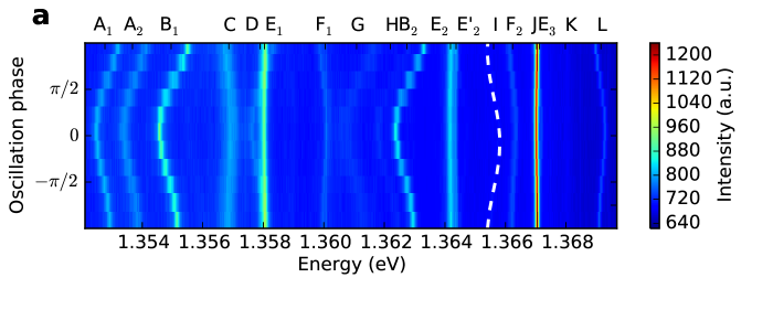
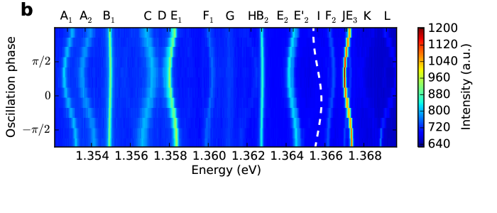
In order to detect the spatially dependent response of the QDs in this oscillating stress field, we realize a stroboscopic optical excitation and detection of the QDs photoluminescence (PL). As shown in Fig.1.b, the radio-frequency generator delivers two RF signals locked in frequency and phase. The first one is harmonic and drives the wire mechanical motion via the PZT; its frequency is chosen to match the X or Y mechanical resonance. The second one is used to gate the laser which excites the QDs PL, and features an ON time times shorter than the mechanical period. The relative phase between both signals can be continuously tuned between and and the resulting stroboscopic QD PL is sent into a high resolution optical spectrometer. By scanning , one obtains series of PL spectra showing how each QD emission frequency is modulated according to the time-dependent stress that they experience. This measurement is carried out for both mechanical polarization directions M = X and Y; the results are shown in Fig. 2.
Upon excitation of the mode M, the emission energy of a given spectral line behaves like
| (1) |
where is the unperturbed emission energy. The measurement of the modulation amplitudes and of the relative phases yields an absolute spatial localization of the QD associated with the spectral line .
As evidenced in Fig. 2, the phase can take two values: or . This phase provides a ‘which side’ information on the location of the emitter with respect to the zero-stress line of mode M. Thus, the couple allows us to place the QD unambiguously in one of the four quadrants defined by the zero-stress lines of modes X and Y (i.e., the and diagonals of the wire section).
In addition, the absolute distances with respect to the zero-stress lines can be inferred from the frequency modulation amplitudes through the relations
| (2) | ||||
| (3) |
We have introduced , the tuning slope of transition . Note that the main contribution (more than ) to the QD energy shift is caused by the component of the strain tensor, since the and components are already one order of magnitude smaller, and that moreover the QD energy shifts caused by these two latter components are times smaller than for the component (see section E of the SI). The quantities and are the (constant) in-plane strain gradients of modes X and Y corresponding to the top facet displacements and respectively. They are given by and , where and are the stress gradient per top facet displacement computed by FEM. Note that, owing to the wire shape anisotropy, we have . For the data shown in this work, we have .
To use this relation, the knowledge of each is in principle required. In the present configuration (local stress applied along the QD growth axis) it has been shown experimentally by some of us Stepanov that the relative dispersion is smaller than . We will thus assume the same for all emitters, equal to the mean value , and include the ’s variations in the location uncertainty analysis.
Interestingly, if the structure embeds a sufficient number of distinct QDs (say N > 10), mapping does not even require an a priori knowledge of . The mapping procedure then consists in two steps. One first determines the QD relative positioning using stroboscopic data (Fig.2). For the relative scaling of the and axes, the top facet vibration amplitudes ratio of both and polarizations is carefully measured. This allows us to express the frequency shift ratio corresponding to the same stress gradient on both and axis as a function of the measured frequency shifts : . In a second step, one determines the overall scaling factor between the relative map and the actual section geometry. We have checked (see section C of the SI) that QDs are optically active over the whole GaAs wire section. Knowing the shape of the waveguide section, we use as a reference the QD which is the closest to the wire sidewall. As described in section D of the SI, the normalized distance of this extremal QD to the sidewall can be determined by a statistical argument and is given by . The standard deviation associated to this estimation scales as .
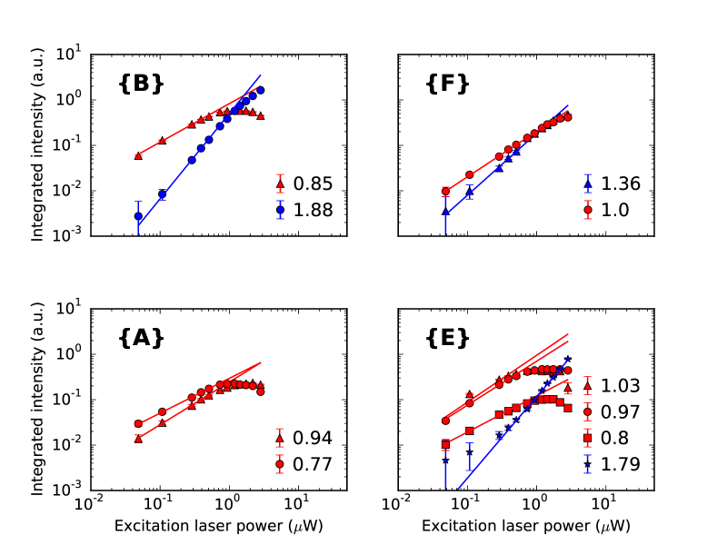
This procedure allows us to construct the map presented in Fig.3, where the labels are consistent with those used for the spectral measurements shown in Fig.2. The insets show that several emission peaks can be found at the same location. Indeed, a single QD can be responsible for one, two or three emission peaks corresponding to the neutral exciton, the charged exciton and the biexcitonic transitions Zhiming . These peaks can be discriminated from each other using their excitation power dependence as described in section B of the SI. When a peak is identified as related to a biexcitonic transition, it always coexists with a neutral or charged exciton peak within the same dot (i.e. at the same position). Note that in this analysis, we have implicitly assumed an identical tuning slope for all three aforementioned transitions. This is indeed correct since for such weak strain fields, the strain induced conduction and valence band shifts dominate over the correction of the many-body Coulomb interaction Kuklewicz ; Wu . With this analysis we could determine that distinct QDs are present in the QDs plane and within our detection spectral window.
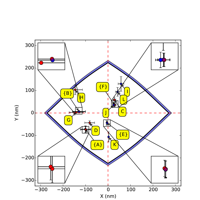
In this mapping procedure, the location of the QDs is found within a certain accuracy, which is fixed by the numerical analysis of the data, as well as by the various assumptions mentioned previously. They can be summarized into several contributions: the measurement accuracy of from the dataset of Fig.2, the statistical determination of the overall scaling factor, the measurement error on the motion amplitude ratio that impacts the relative scaling on the and axes, the non perfectly constant stress gradient , and finally, the non-exactly equal response ’s of each QDs to an equal stress. A detailed analysis of these contributions on the location accuracy of the QDs is given in section F of the SI. Note that while the total relative uncertainties vary little between QDs, the absolute uncertainties will be smaller for QDs closer to the neutral lines (see Fig.3). With this non-destructive method, we are able to determine the QDs positions inside the nanowire with an uncertainty as small as nm, when it is close to a neutral line, and of at most nm, close to the edges. This is to be compared to the diameter on the order of nm of a QD. This highest uncertainty value corresponds only to of the QD emission wavelength. Strikingly, the smallest uncertainty corresponds to as little as of the QDs emission wavelength.
It turns out that the largest source of uncertainty comes from the dispersion in the response of each QD to a given stress. However, it would be possible, with a different set-up, to measure each independently by exciting the longitudinal breathing mode (at MHz) which features a uniform strain within the QD plane. The measured energy shift of each QDi would then provide us with an in situ measurement of . Within realistic assumptions, this would reduce the errors bars down to nm close to the center and nm close to the edge.
Beyond QD devices, this very accurate non-destructive imaging method generalizes to any solid state quantum emitter sensitive to strain such as color centers like NV centers Teissier or rare earth ions Thorpe . The knowledge of quantum emitters positions with respect to each other, as well as with respect to a fixed point in space, opens up new possibilities to characterize and exploit many body quantum optics with such objects, as well as their interaction with nearby surfaces or nanostructures, engineered or unwanted.
Methods
Structure fabrication and geometry
The GaAs photonic wire used in this experiment was fabricated from a planar sample grown by molecular beam epitaxy over a GaAs [001] wafer. The photonic wires are defined by a top-down approach, which employs in particular e-beam lithography and a carefully optimized dry-etching step, conducted in a reactive ion etching chamber Munsch . From the top facet to the base waist, the length of the GaAs conical wire is . The top facet is circular and features a diameter of . Slightly different etching rates along different crystallographic directions result in a base which features a lozenge shape. Its geometry was determined by FIB milling and SEM observation (see section A of the SI). Its major diagonal, oriented along the direction, features a length of nm. The minor diameter is oriented along , with a length of nm. This shape anisotropy splits the first flexural mode into two mechanical modes X and Y of orthogonal polarization directions. The wire embeds a single layer of self-assembled InAs QDs, which is located above the bottom end of the conical wire; the structure typically embeds a few tens of quantum dots. The wire sidewalls are covered by a nm thick Si3N4 passivation layer Yeo_2011 , and the top facet is covered by a nm thick Si3N4 layer.
Mechanical spectroscopy
In order to excite and characterize the nanowire vibration, a piezoelectrical transducer (PZT) is placed at the back side of the sample-holder. The PZT is driven by a sinusoidal voltage, the frequency of which can be scanned across the mechanical resonance. Mechanical spectroscopy of the wire motion is realized by illuminating the wire top facet with a laser, and by measuring the reflected beam deviation with the difference signal from a split photodiode (SPD) Yeo ; Sanii ; Gloppe . The polarization of these mechanical modes is experimentally determined by rotating the nanowire top facet image with a Dove prism, prior to detection with the SPD.
Acknowledgements
The authors wish to thank E. Gautier for the FIB cut and images. Sample fabrication was carried out in the Upstream Nanofabrication Facility (PTA) and CEA LETI MINATEC/DOPT clean rooms. P.-L. de Assis was financially supported by the ANR-WIFO project and CAPES Young Talents Fellowship Grant number 88887.059630/2014-00, and D. Tumanov by the Rhône-Alpes Region.
References
- (1) Rittweger, E., Han, K.Y., Irvine, S.E., Eggeling, C. and Hell, S. W., STED microscopy reveals crystal colour centres with nanometric resolution. Nature Photon. 3, 144-147 (2009)
- (2) Bakr, W. S. et al., A quantum gas microscope for detecting single atoms in a Hubbard-regime optical lattice. Nature 462, 74 (2009)
- (3) Trotta, R. and Rastelli, A., Engineering of quantum dot photon sources via electro-elastic fields. in Engineering the Atom-Photon Interaction (Spinger, 2015)
- (4) Yeo, I., et al., Strain-mediated coupling in a quantum dot-mechanical oscillator hybrid system. Nature Nanotech. 9, 106 (2014)
- (5) Montinaro, M., Wüst, G., Munsch, M., Fontana, Y., Russo-Averchi, E., Heiss, M., Fontcuberta i Morral, A., Warburton, R. J. and Poggio, M., Quantum Dot Opto-Mechanics in a Fully Self-Assembled Nanowire. Nano Lett. 14, 4454-4460 (2014)
- (6) Gérard, J.-M. Sermage, B. , Gayral, B., Legrand, B., Costard, E., Thierry-Mieg, V., Phys. Rev. Lett 81, 1110 (1998)
- (7) Lodahl, P., Mahmoodian, S. and Stobbe, S., Interfacing single photons and single quantum dots with photonic nanostructures. Rev. Mod. Phys. 87, 347 (2015)
- (8) Claudon, J., Bleuse, J., Malik, N.S., Bazin, M., Jaffrennou, P., Gregersen, N., Sauvan, C., Lalanne, P., Gérard, J.M., A highly efficient single-photon source based on a quantum dot in a photonic nanowire. Nature Photon. 4, 174-177 (2010)
- (9) Munsch, M., et al., Dielectric GaAs Antenna Ensuring an Efficient Broadband Coupling between an InAs Quantum Dot and a Gaussian Optical Beam. Phys. Rev. Lett. 110 177402 (2013)
- (10) Dousse, A. et al., Ultrabright source of entangled photon pairs. Nature 466, 217 (2010)
- (11) Ding, X. et al., On-Demand Single Photons with High Extraction Efficiency and Near-Unity Indistinguishability from a Resonantly Driven Quantum Dot in a Micropillar. Phys. Rev. Lett. 116, 020401 (2016)
- (12) Besombes, L., et al., Probing the Spin State of a Single Magnetic Ion in an Individual Quantum Dot. Phys. Rev. Lett. 93, 207403 (2004)
- (13) Awschalom, D. D. et al., Quantum Spintronics: Engineering and Manipulating Atom-Like Spins in Semiconductors. Science 339, 1174 (2013)
- (14) De Greve, K. et al. Quantum-dot spin-photon entanglement via frequency down conversion to telecom wavelength. Nature 491, 421 (2012)
- (15) Gao, W. B. et al. Observation of entanglement between a quantum dot spin and a single photon. Nature 491, 426 (2012)
- (16) Unold, T. et al., Optical Control of Excitons in a Pair of Quantum Dots Coupled by the Dipole-Dipole Interaction. Phys. Rev. Lett. 94, 137404 (2005)
- (17) Parascandolo, G. and Savona, V., Long-range radiative interaction between semiconductor quantum dots. Phys. Rev. B 71, 045335 (2005)
- (18) Kasprzak, J., Patton B., Savona V., and Langbein W., Coherent coupling between distant excitons revealed by two-dimensional nonlinear hyperspectral imaging. Nature Photon. 5, 123 (2011)
- (19) Mermillod, Q., Jakubczyk, T., Delmonte, V., Delga, A., Peinke, E., Gérard, J.-M., Claudon, J. and Kasprzak, J., Harvesting, Coupling, and Control of Single-Exciton Coherences in Photonic Waveguide Antennas. Phys. Rev. Lett. 116, 163903 (2016)
- (20) Temnov, V. V. and Woggon U., Superradiance and Subradiance in an Inhomogeneously Broadened Ensemble of Two-Level Systems Coupled to a Low-Q Cavity. Phys. Rev. Lett. 95, 243602 (2005)
- (21) Auffèves, A., Gerace, D., Portolan, S., Drezet, A., and França Santos, M., Few emitters in a cavity: from cooperative emission to individualization. New J. Phys. 13, 093020 (2011)
- (22) Betzig, E., and Chichester, R. J., Single Molecules Observed by Near-Field Scanning Optical Microscopy. Science 262, 1422-1425 (1993)
- (23) Matsuda, K. et al., Near-field optical mapping of exciton wave functions in a GaAs quantum dot. Phys. Rev. Lett. 91, 177401 (2003)
- (24) Brown, R. W., Norman Cheng, Y.-C., Haacke, E. M., Thompson, M. R., and Venkatesan, R., Magnetic Resonance Imaging: Physical Principles and Sequence Design (John Wiley & Sons, New York City, 2014)
- (25) Mamin, H.J. et al., Nanoscale Nuclear Magnetic Resonance with a Nitrogen-Vacancy Spin Sensor. Science 339, 557 (2013)
- (26) Degen, C.L., Poggio, M., Mamin, H.J., Rettner, C.T., and Rugar, D., Nanoscale magnetic resonance imaging. Proc. Nat. Acad. Sci. 106, 1313 (2009)
- (27) Sanii, B., and Ashby, P.D., High Sensitivity Deflection Detection of Nanowires. Phys. Rev. Lett. 104, 147203 (2010)
- (28) Gloppe, A., Verlot, P., Dupont-Ferrier, E., Siria, A., Poncharal, P., Bachelier, G., Vincent, P., and Arcizet, O., Bidimensional nano-optomechanics and topological backaction in a non-conservative radiation force field, Nature Nanotechnology 9, 920, (2014)
- (29) Stepanov, P., Elzo-Aizarna, M., Bleuse, J., Malik, N.S., Curé, Y., Gautier, E., Favre-Nicolin, V., Gérard, J.M., and Claudon, J., Large and Uniform Optical Emission Shifts in Quantum Dots Strained along Their Growth Axis. Nano Lett. 16, 3215-3220 (2016)
- (30) Wang, Z. M., Self-Assembled Quantum Dots (Springer-Verlag, New York City, 2008)
- (31) Kuklewicz, C. E., Malein, R. N. E., Petroff, P. M., and Gerardot B. D., Electro-Elastic Tuning of Single Particles in Individual Self-Assembled Quantum Dots. Nano Lett. 12, 3761 (2012)
- (32) Wu, X., Dou, X., Ding K., Zhou, P., Ni, H., Niu, Z., Jiang, D., and Sun B., In situ tuning the single photon emission from single quantum dots through hydrostatic pressure. Appl. Phys. Lett. 103, 252108 (2013)
- (33) Teissier, J., Barfuss, A., Appel, P., Neu, E., Maletinsky, P., Strain Coupling of a Nitrogen-Vacancy Center Spin to a Diamond Mechanical Oscillator, Phys. Rev. Lett. 113, 020503 (2014)
- (34) Thorpe, M.J., Rippe, L., Fortier, T.M., Kirchner, M.S., Rosenband, T., Frequency stabilization to via spectral-hole burning, Nature Photon., 5, 688 (2011)
- (35) Yeo, I., et al., Surface effects in a semiconductor photonic nanowire and spectral stability of an embedded single quantum dot. Appl. Phys. Lett. 99, 233106 (2011)
Supplementary information
.1 Geometry of the mechanical oscillator
The fact that the first flexural mode of the photonic wire is split into two orthogonal directions with significantly different frequencies indicates that there is an intrinsic asymmetry to its shape. This is confirmed by SEM images of a wire cut by a focused ion beam (FIB), indicating a cross-section at the anchorage that can be well approximated by a lozenge with long semi-axis and short semi-axis , so that (see Supplementary Fig.4).
The transition from a lozenge at the bottom to a circle of radius at the top of the nanowire (m) means that at the level of the QDs the cross-section has a shape that can be determined by connecting every point on the bottom () to its corresponding point on the top of the wire (at m) by a straight line. This is done by parametrizing both the lozenge and the circle in polar coordinates, as functions of , so that for each line both start and end points have the same . Thus, for any given position in the axis it is possible to determine the shape of the cross-section, which we call a bulged lozenge.
At , the coordinates of the wire section are given by
| (4) | |||||
| (5) |
with
| (6) |
and
| (7) |
At an elevation , the wire section is given by
| (8) | |||||
| (9) | |||||
| (10) |
Using data from the FIB cut images and finite element simulations to compare theoretical and measured mechanical frequencies, we estimate and , so that . The QD plane is at , as determined during the epitaxial growth of the sample used to fabricate the photonic wires.
.2 Identification of emission lines
As seen in Fig.3 of the main text, many emission lines correspond to spatial location overlapping in the photonic wire. This is due to the fact that excitonic, biexcitonic and trionic lines of the same QD appear with the laser power used to perform the stroboscopic experiment.
In order to determine which emission lines correspond to excitons and which correspond to biexcitons, we recorded a series of photoluminescence spectra using a wide range of excitation-laser powers. Each line mapped in Fig.3 of the main text was then analysed with respect to the dependence of their integrated intensity with excitation power, . Excitons exhibit , with sub-linearity being attributed to charge trapping and other effects that hamper radiative recombination. It is important to note that charged excitons may also exhibit a sub-linear power dependence. Biexcitons, on the other hand, are associated with ; the inequality being due to the same kind of effects that cause a sub-linear power-dependence for excitonic emission intensity.
In Supplementary Fig.5 we show how the emission intensity depends on excitation power for the families of emission lines highlighted in the insets of Fig.3 of the main text. These families of lines are also indicated in Fig.2 of the main text.
.3 Determination of the “dead layer” thickness
The wire etching process introduces defect close to its surface. Light emission of QDs located close to the outer surface might be suppressed owing to non-radiative recombinations caused by the surface proximity. Geometrically, such a “dead layer” corresponds to all points in the QD plane that are at a distance from at least one point on the wire boundary. The measure of this dead layer thickness is important to know the effective area where active QDs are located (see section .4).
This effective boundary will have the same general shape as the outer boundary, with a scaling factor given by the ratio between and , where is the point on the axis that is at a distance from two points on the outer boundary (see Supplementary Fig.6). Given the non-circular nature of the cross section, and is given by
| (11) |
where is the angular position of the two points tangent to the circle of radius centered on in Supplementary Fig.6. In order to properly determine , we have to solve
| (12) |
where is the angle that the vector normal to the boundary at a point makes with the axis:
| (13) |
The thickness of this “dead layer” is inferred by counting the number of emission lines within a given spectral window for wires with different top radii (see Supplementary Fig.7). We have taken photoluminescence spectra of wires with different diameters, using the same spectral window and pumping non-resonantly above the saturation power of the faintest QDs, to assure that none would be ignored due to insufficient excitation.
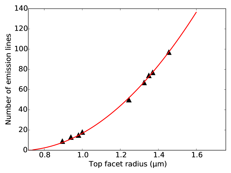
We considered all emission lines in each PL spectrum and fitted the number of lines as a function of the top facet radius, . It is possible to calculate the shape the cross section at the level of the QDs for any , by using the transformations , , and . is the top radius of a given wire and is the top radius of the one used in our experiment, for which and are known.
The fit was done using
| (14) |
with being the function that determines the inner boundary at the level of the QDs for a wire of top radius , given a “dead layer” of thickness and a QD surface density .
The two fitting parameters are the emission line surface density and the maximal radius of a photonic wire that would present no emitting QD, . The fit gives and , with uncertainties corresponding to the standard deviation of each fitted parameter.
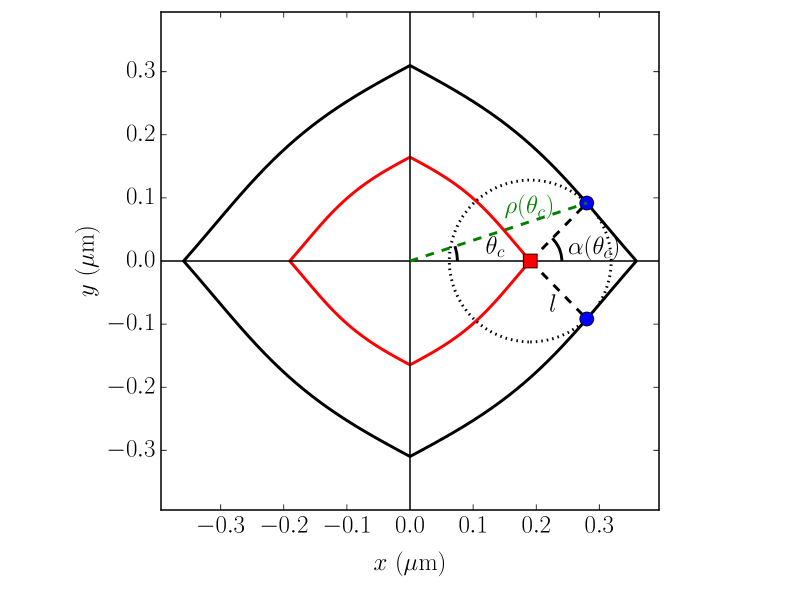
.4 Probabilistic estimation of position for the QD closest to the edge
In order to determine a scaling factor that properly converts the energy shifts caused by mechanical stress into an position, we have estimated, for QDs randomly distributed on the optically active area of the wire, the expected position of the QD located closer to the border of the dead layer. As Supplementary Fig.8 shows, this QD, called QDm, will be on a concentric bulged lozenge described by , where describes the dead layer border. The other QDs are then located inside this lozenge of area , where is the optically active surface of the QD plane (at an elevationm). The probability for a QD to be inside that lozenge is given by the ratio of the areas. The probability for QDs being inside that bulged lozenge is therefore .
The probability for finding a QD in the area between bulged lozenges parameterized by and , in the hashed region of Supplementary Fig.8, is . For finding any of the QDs in this area the probability is . The overall probability of finding a QD in this area and all the other QDs inside the region of is then given by
| (15) |
We can compute the expected value for the extremal QD, together with its standard deviation, using the definitions of the expected value and variance:
| (16) |
and the corresponding statistical uncertainty
| (17) |
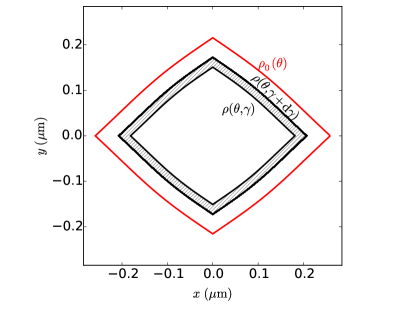
Experimentally, we measure the spectral shifts and along the and polarisations for each QD. The QD closest to an edge of the bulged lozenge will be QDm and positioned on the lozenge. This will determine the absolute position of QDm within the wire section. In our case, we find that QDm is the QD labelled H on the map given in Fig.3 of the main text. It corresponds to nm.
For the final value of , we have to account for the dead layer estimation (cf section .3 above), and we finally obtain nm.
.5 Impact of external stress on the QD emission energy
We derive here a simple analytical estimation of the impact of external stress on the emission energy of a self-assembled QD grown along the direction. To a very good approximation, the stress response is dominated by single-particle effects, i.e., by a modification of single electron and hole energy levels. The QD emission energy can then be expressed as , where is the heavy hole (hh) bandgap of the QD material; and are the energies of the confined electronic and hh levels, measured with respect to the edge of the QD material bands.
We first determine the shift of the hh bandgap induced by a ‘small’ external stress. In a self-assembled QD, the QD material experiences a large intrinsic bi-axial compressive strain, which strongly lifts the degeneracy of heavy and light hole bands. Following Ref. StepanovSI , we apply first-order perturbation theory to the Bir-Pikus Hamiltonian and obtain , with (with the convention and ) and the deformation potentials of the QD material Yu ; Vurgaftman ; and are respectively the hydrostatic and the tetragonal shear strain induced by the external stress. We use here the cubic basis ().
To estimate the shifts and of the electron and hole confined levels, we model our flat-lens QD as a quantum well of thickness . For a weakly bounded electronic level, . A similar expression is obtained for the hole level, by replacing the conduction band offset (CBO) by the valence band offset (VBO), and by . CBO, VBO, can be obtained from a modelling of the QD. and are determined with the deformation potentials: and . , and are the difference between the deformation potentials of the barrier and QD materials. Finally, .
To obtain numerical values, we consider an In0.6Ga0.4As/GaAs QD and use the QD energy levels presented in Ref. JonsSI . GaAs is treated as a mechanically isotropic material, with a Poisson ratio and a Young modulus GPa. A uniaxial stress applied along yields , and . A uniaxial stress applied along yields , and . This analysis yields several important conclusions: (i) For small stresses associated with the wire vibration, the QD emission shift is only due to the diagonal components of the stress tensor (, and ). (ii) For uniaxial stresses applied along the , and directions, the QD emission shift is dominated by the shift of the hh bandgap of the QD material. Shifts associated with confinement effects are typically times smaller. (iii) The tuning slope for uniaxial stress applied along is . It exceeds the one for a uniaxial stress applied along or (), by a factor of . Along the direction, the effects of and add constructively to induce a large hh bandgap shift. In contrast, the effect of partially cancels the one of when the stress is applied along or .
We have used a commercial finite element modelling software to compute the stress components , , and obtain the QD energy shift at any location. We find that the typical QD energy shift for a nm top facet displacement is of for QD located nm away from the zero-stress line. The linearity of the shift with respect to the distance from the zero-stress line is better than .
.6 Experimental uncertainty on the spatial coordinates
As discussed in the main text, the coordinate of the quantum dot QDi is obtained from the spectral modulation amplitude , via the following formula :
| (18) |
with
| (19) |
so that the variance is given by
| (20) |
We know from StepanovSI that . From the FEM calculation that we have performed, the uniformity of the gradient is guaranteed up to . In the first term of eq. 20, the factor of comes from the fact that and . We have seen in section .4 above that nm.
The variance of is given by
| (21) | |||||
where is the uncertainty extracted from the fit of the stroboscopic data of Fig.2 of the main text for QDi. These fits have been realized by taking into account a linear drift of the wire mechanical frequency during the acquisition of the stroboscopic spectra, leading to a linear phase drift. The quantity is the uncertainty in the and motion amplitude ratio.
The uncertainty budget is given in Supplementary Fig.9. It appears that the main contribution comes from the dispersion on QD responses .
References
- (1) Stepanov, P., Elzo-Aizarna, M., Bleuse, J., Malik, N.S., Curé, Y., Gautier, E., Favre-Nicolin, V., Gérard, J.M., and Claudon, J., Large and Uniform Optical Emission Shifts in Quantum Dots Strained along Their Growth Axis. Nano Lett. 16, 3215 (2016)
- (2) Yu, P.Y., and Cardona, M., Fundamentals of semiconductors. Springer ed. (2010)
- (3) Vurgaftman, I., Meyer, J.R., Ram-Mohan, L.R., Band parameters for III-V compound semiconductors and their alloys, J. Appl. Phys. 89, 5815 (2001)
- (4) Jöns, K.D., Hafenbrak, R., Singh, R., Ding, F., Plumhof, J.D., Rastelli, A., Schmidt, O.G., Bester, G., and Michler, P., Dependence of the Redshifted and Blueshifted Photoluminescence Spectra of Single InxGa1-xAs/GaAs Quantum Dots on the Applied Uniaxial Stress. Phys. Rev. Lett. 107, 217402 (2011)