Spatially inhomogeneous electron state deep in the extreme quantum limit of strontium titanate
Abstract
When an electronic system is subjected to a sufficiently strong magnetic field that the cyclotron energy is much larger than the Fermi energy, the system enters the “extreme quantum limit” (EQL) and becomes susceptible to a number of instabilities. Bringing a three-dimensional electronic system deeply into the EQL can be difficult, however, since it requires a small Fermi energy, large magnetic field, and low disorder. Here we present an experimental study of the EQL in lightly-doped single crystals of strontium titanate, which remain good bulk conductors down to very low temperatures and high magnetic fields. Our experiments probe deeply into the regime where theory has long predicted electron-electron interactions to drive the system into a charge density wave or Wigner crystal state. A number of interesting features arise in the transport in this regime, including a striking re-entrant nonlinearity in the current-voltage characteristics and a saturation of the quantum-limiting field at low carrier density. We discuss these features in the context of possible correlated electron states, and present an alternative picture based on magnetic-field induced puddling of electrons.
When subjected to a sufficiently strong magnetic field, the bulk properties of an electronic system change dramatically. In particular, a three-dimensional electron gas acquires very different behavior when the magnetic field becomes large enough that the cyclotron energy exceeds the Fermi energy . (Here, is the cyclotron frequency, is the reduced Planck constant, is the electron charge, is the effective electron mass, and is the electron density.) In this “extreme quantum limit” (EQL) electron motion in the directions perpendicular to the magnetic field is quantized, and all electrons occupy only the lowest Landau level. Semi-classically, one can visualize the EQL as the state in which electron trajectories are tight spirals along the field direction, with gyration radius that is much shorter than the typical inter-electron spacing.
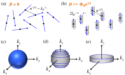
As a consequence of this quantization by magnetic field, in the EQL the electron kinetic energy retains a dependence only on the momentum parallel to the field, and the Fermi surface takes the form of two parallel rings in momentum space [see Fig. 1(e)]. For a clean, low-temperature electron gas, such a dimensionally reduced dispersion implies a number of potentially competing instabilities, including spin or valley density wave, charge density wave (CDW), and Wigner crystallization.Celli and Mermin (1965); Kaplan and Glasser (1972); Kleppmann and Elliott (1975); Halperin (1987)
Such a high-field situation, however, is difficult to realize experimentally. For a typical metal, for example, the EQL requires fields on the order of T, and is thus relevant only for extreme astrophysical settings.Lai (2001); Kaplan and Glasser (1972) Realization of the EQL in the laboratory requires a material that can exhibit metallic behavior at very low electron density .
Doped bulk strontium titanate, SrTiO3 (STO), is such a material. STO, a semiconducting perovskite oxide, has been studied intensively in recent years, with much attention devoted to its potential in thin films and heterostructure devices.Haeni et al. (2004); Ohtomo and Hwang (2004); Thiel et al. (2006); Caviglia et al. (2008); Son et al. (2010) But as a bulk material STO has attracted interest for over half a century,Cowley (1964); Barrett (1952); Frederikse et al. (1967); Yamada and Shirane (1969); Neville et al. (1972); Kahn and Leyendecker (1964); Schooley et al. (1964) largely because of its anomalous dielectric response at low temperature.Cowley (1964); Yamada and Shirane (1969); Neville et al. (1972) Indeed, STO has a static, long-wavelength dielectric constant that reaches at low temperatures (with a weak directional dependenceNeville et al. (1972)). One implication of this enormous dielectric constant is that the effective Bohr radius associated with shallow donor states becomes extremely large: nm. Consequently, in the absence of compensating acceptors, even a very small concentration of electron donors is sufficient to ensure that STO is on the conducting side of the Mott criterion, .Mott (1968) Importantly, as we discuss below, this large dielectric constant also implies a significant robustness against localization by charge disorder.
In this paper we present a clear experimental realization of a deep-EQL state in STO. Using transport measurements at low temperatures and high magnetic fields, we probe deeply into the EQL in a number of low-carrier-density samples. Our samples remain good bulk conductors throughout our measurement conditions, and at large magnetic fields they exhibit a strong, re-entrant nonlinearity in the resistivity. This nonlinearity is discussed in the context of possible correlated electron states, and an alternate picture is presented based on puddling of electrons in disorder potential wells.
Crucial to our study is the existence of a strong hierarchy of energy scales:
| (1) |
Here, is the effective Rydberg energy and is the thermal energy. The first inequality in Eq. (1) is equivalent to the large magnetic field condition explained above, while the second set of inequalities guarantees that the electron state deep in the EQL is not destroyed either by thermal excitation or by freezeout of electrons onto donor impurities. While previous high-field studies have managed to approach or even enter the EQL in doped semiconductors, simultaneously achieving both sets of inequalities in Eq. (1) has been more challenging. For example, studies of the EQL in narrow band gap semiconductors, such as -type InAs,Zeitler et al. (1994) InSb,Murzin et al. (2000); Shayegan et al. (1988); Mani (1989); Zeitler et al. (1994) and HgCdTe,Shayegan et al. (1988); Mani (1989) are generally limited to the case where and are similar in magnitude. Consequently, in these materials electrons freeze onto donor impurities shortly after the EQL is reached, and achieving a deep-EQL electron state is not possible. Previous high-field studies of STO have also generally failed to satisfy this hierarchy, either because the temperature was too high to satisfy the second inequalityKozuka et al. (2008) or because the Fermi energy was too high to satisfy the first.Allen et al. (2013); Lin et al. (2013)
In our study, we examine millimeter-sized STO single crystals (dimensions: mm), obtained from CrysTec GmbH.cry ,111This commercial product is described in this paper in order to specify adequately the experimental procedure. In no case does such identification imply recommendation or endorsement by the National Institute of Standards and Technology, nor does it imply that it is necessarily the best available for the purpose. In order to introduce a finite concentration of conduction-band electrons, the samples were heated within a vacuum chamber following the protocol described in the Supplementary Information (SI). This heating process is known to produce oxygen vacancies within the sample volume, which act as electron donors.De Souza et al. (2012); Paladino (1965),222In principle, a single oxygen vacancy acts stoichiometrically as a double-donor, but it is generally accepted that one of the two electron states remains tightly bound to the doubly-charged oxygen ion, so that the vacancy donates only a single electron to the conduction band.Janotti et al. (2014) The heating temperature was varied from one sample to another in order to produce samples with different doping levels. For the samples that are the focus of this study, the resulting carrier densities ranged from cm-3 to cm-3. (Here and below, all listed values of the experimental uncertainty correspond to confidence intervals.)
Importantly, in addition to the oxygen vacancies, as-grown STO crystals are known to have a significant concentration of additional impurities, mostly Fe and Al, that act as deep acceptors.Ensign and Stokowski (1970); Morin and Oliver (1973) Indeed, previous studies based on chemical analysis and secondary ion mass spectroscopyDe Souza et al. (2012) have shown these impurities to be present at the level of cm-3. Since this concentration is significantly larger than the measured carrier density , our samples can be described as almost-completely-compensated semiconductors, for which the number of donors and acceptors are nearly identical and thus the total concentration of charged impurities is much larger than . This relatively large concentration of impurities is also consistent with the measured zero-field mobility, which suggests an impurity concentration on the order of cm-3 (as shown in SI Sec. II). The consequences of the impurity concentration for transport are discussed in detail below.
As the magnetic field is increased from zero, the longitudinal resistivity exhibits Shubnikov-de Haas (SdH) oscillations, as higher Landau levels are pushed outside the Fermi surface with increasing field. In particular, the field at which the th Landau level becomes depopulated followsAbrikosov, Alexei A (1988)
| (2) |
where is the flux quantum, and the second equality in Eq. (2) corresponds to the usual limit of large . As shown in Fig. 2, the observed oscillations of resistivity are periodic in , suggesting a single, small electron pocket of Fermi surface.Lin et al. (2015) The position of the final () oscillation indicates that the EQL is reached at fields T to T, varying from sample to sample. Here the field is defined experimentally as the position in magnetic field of the th local maximum of resistance, counted in order of decreasing magnetic field. The identification of these maxima is facilitated by subtracting a smooth, fourth order polynomial from the vs. curve, as shown in Fig. 2(b) (see also SI Sec. IV). The period of oscillation is also confirmed by the periodicity of the first derivative of vs. [see Fig. 2(c)]. Plotting against the Landau index , as shown in Fig. 2(c), indicates unambiguously that each of our samples is well within the EQL at our largest magnetic fields. 333One can note that Eq. (2) assumes that Landau levels are not spin-degenerate. The agreement of this equation with our measurements suggests that this is indeed the case in our samples for all appreciable magnetic fields. This non-degeneracy can be expected if one assumes that the electron -factor in STO is of order unity. In this case the Zeeman energy is of order eV per Tesla of field, while the Fermi energy in our samples is in the range eV to eV, so that the conduction electrons become completely spin polarized even at relatively high Landau levels.
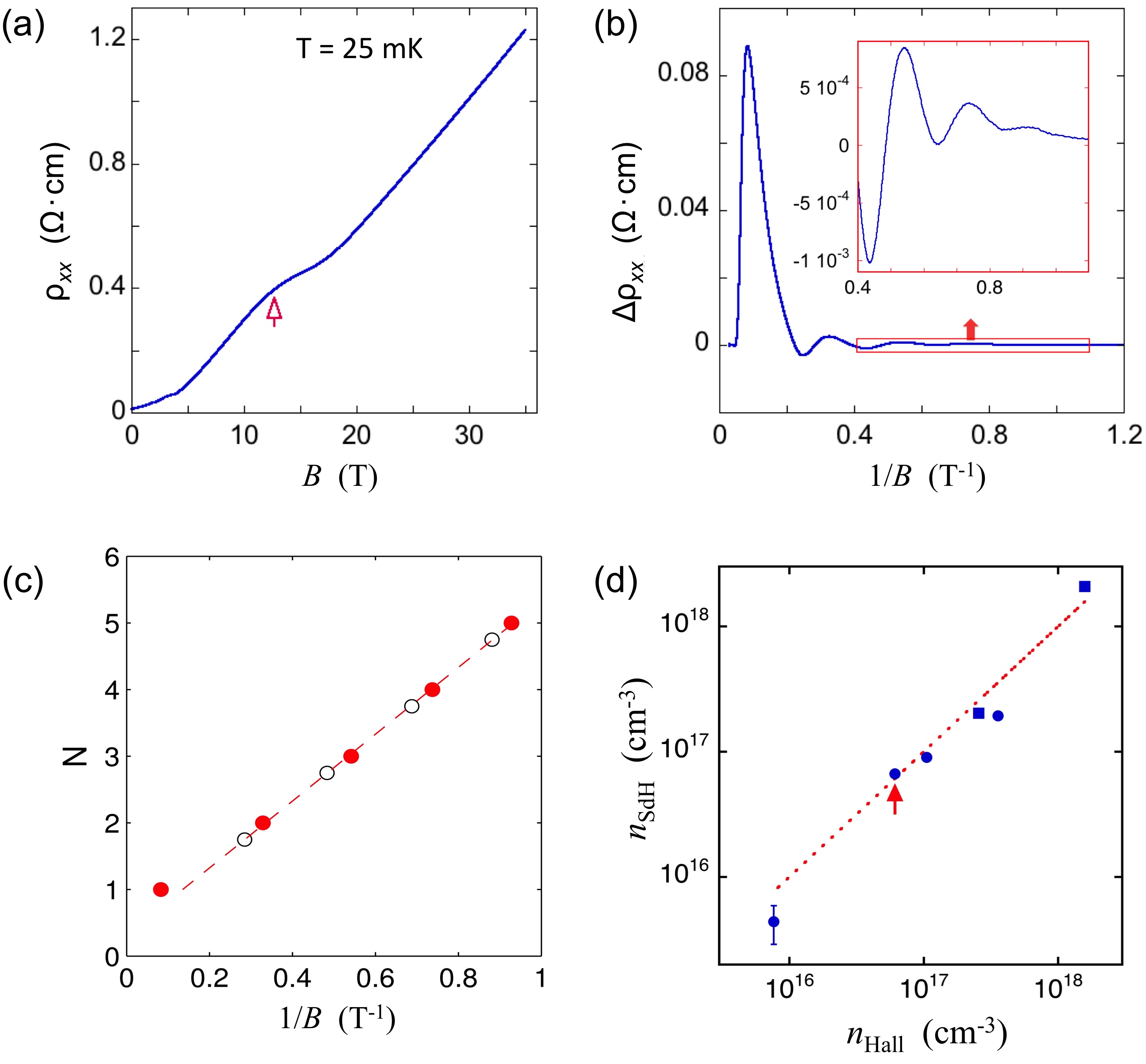
Using Eq. (2), the value of the SdH period gives a measure of the electron density . The excellent linear fit to Eq. (2) indicates that the large- approximation is appropriate for all . Further, the inferred value of closely matches the value obtained from Hall effect measurements, as shown in Fig. 2(d). The agreement between the two measures of suggests that electrons are uniformly distributed through the bulk of the STO crystal, since the SdH measurements are sensitive to the average Fermi energy of electrons in the sample, while the Hall effect observes only the thickness-averaged number of carriers. The period of the SdH oscillations is also independent of whether the magnetic field is aligned parallel or perpendicular to the current, as shown in Fig. 3(a), which confirms the three-dimensional nature of the electron system. We do, however, observe a noticeable anisotropy in the magnetoresistance (MR) at large fields, as shown in Fig. 3(b).
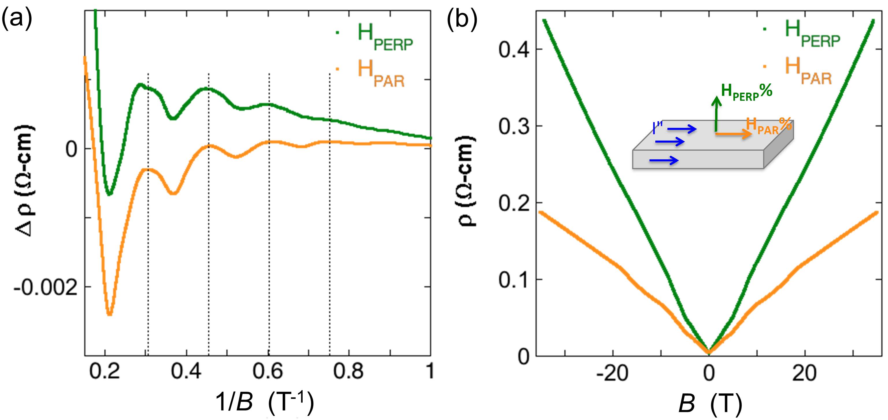
Our samples also exhibit a large linear MR in the EQL, as evidenced in Figs. 2(a) and 3(b), which show a MR ratio . Such non-saturating, linear MR is commonly associated with semi-classical drift of electron orbits along contours of a disorder potential with a long correlation length,Murzin (2000); Song et al. (2015) or with strong spatial inhomogeneity of the carrier concentration or mobility.Dykhne (1971); Parish and Littlewood (2005); Kozlova et al. (2012) Below we provide an additional comment on these possibilities.
While the Fermi energy of a three-dimensional electron gas is essentially constant at small values of the magnetic field, once the EQL is reached (after the last SdH oscillation) the Fermi energy acquires a strong dependence on the field strength. In particular, in the EQL , as constriction of electronic wave functions in the perpendicular directions reduces their quantum overlap and causes the Fermi energy to drop. In our samples, is small enough that in the EQL only the lowest band is relevant,Khalsa and MacDonald (2012); Allen et al. (2013) and this is consistent with the single frequency observed in the low field SdH measurement.444This lowest band has a slight anisotropy of the effective mass,Allen et al. (2013) resulting from the tetragonal distortion of the STO lattice at low temperature, so for the sake of making numerical estimates below we take the effective mass to be equal to the geometric mean of the three perpendicular masses, which gives , where is the bare electron mass.
As the Fermi energy decreases with increasing field, the relative strength of the Coulomb interaction grows, as described by the ratio , where is the typical strength of the Coulomb interaction between neighboring electrons in the field direction, and is the Fermi energy. Here, is the Fermi wave vector in the field direction, so that one can write . At large , a clean, low-temperature electron gas becomes unstable with respect to the formation of a CDW or Wigner crystal. In our experiments is as large as , which is two orders of magnitude larger than in previous high-field experiments in STO.Allen et al. (2013); Lin et al. (2013) At such large values of , Hartree-Fock calculations predict a CDW gap that exceeds the Fermi energy, indicating a strong instability toward a spatially inhomogeneous phase.Fukuyama (1978); Gerhardts (1980)
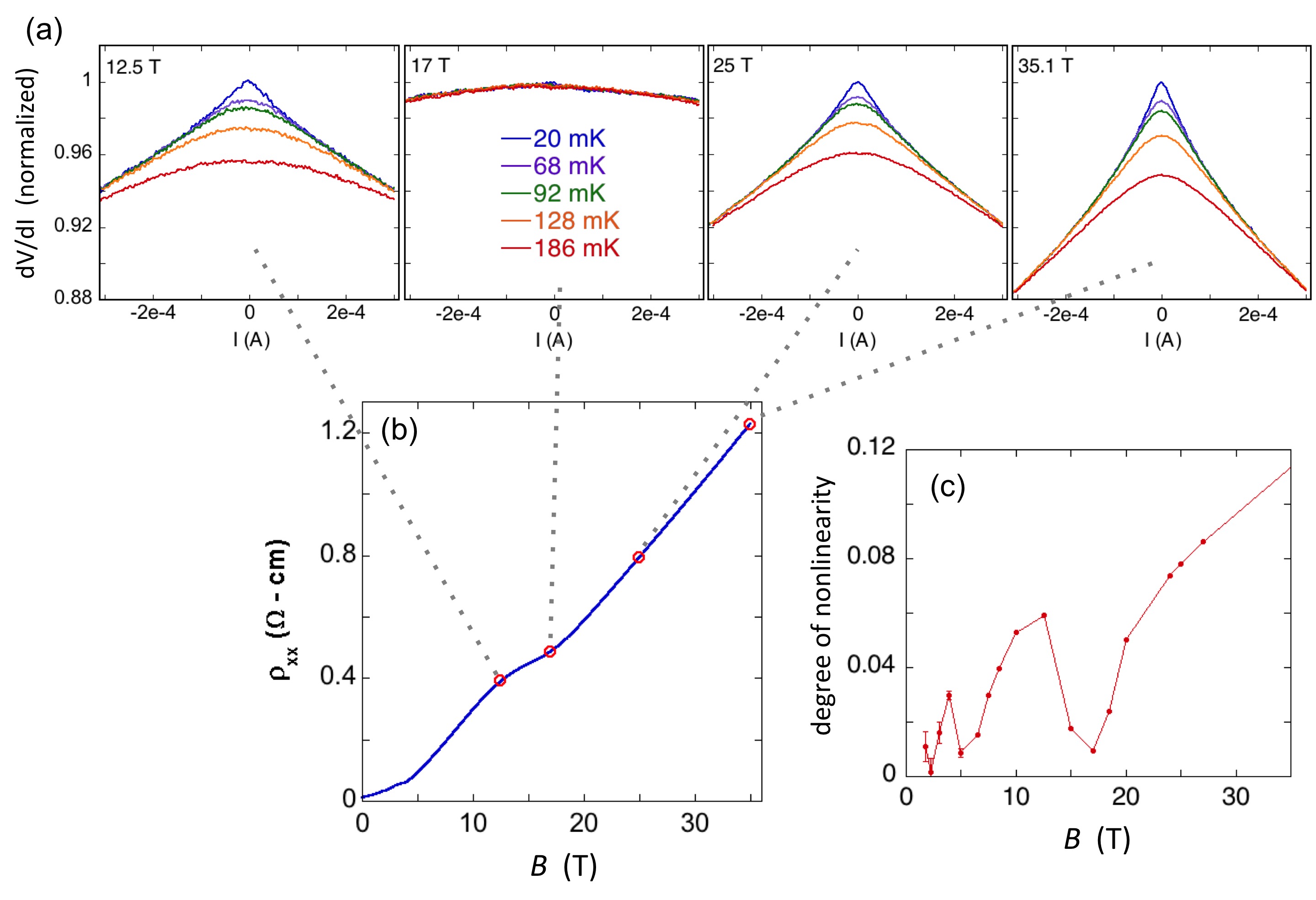
Deep within the EQL, we observe a significant nonlinearity in the current-voltage (-) characteristics, as illustrated in Fig. 4(a). Such nonlinearity typically implies “pinning” or trapping of carriers by a disorder potential. The observed nonlinearity is also weaker at higher temperatures, while the zero bias resistance is lower, implying weaker pinning as temperature is increased. A careful examination of the power dissipation at low bias confirms that the nonlinearity is not a result of Joule heating, particularly at low bias (see SI Sec. I). We also find it unlikely that the nonlinearity arises from scattering by domain walls separating tetragonal domains, which form below K as STO undergoes a transition from cubic to tetragonal crystal symmetry.Cowley (1964) The nonlinearity that we measure is clearly dependent on the magnetic field strength, while such a domain structure is -independent. We also observe no sign of any anomalies in the resistivity at K (see SI Sec. V).
Strikingly, the observed nonlinearity appears in a re-entrant way at lower magnetic fields, becoming most pronounced at relative resistivity maxima and disappearing at relative resistivity minima. This is illustrated in Fig. 4(c). It is worth noting that a similar re-entrant nonlinearity has been observed in both NbSe3 and InAs, although in both cases observations were limited to relatively high Landau levels. In NbSe3 the results were interpreted in terms of CDW physics,Richard et al. (1987) while in InAs it was explained in terms of changes in the effective electron temperature.Bauer and Kahlert (1972) A closer analysis of the nonlinearity is presented in SI Sec. V, including the scaling of the resistivity with bias voltage and magnetic field.
Strong nonlinearity in the transport is expected when electrons form a spatially-correlated state, such as a CDW or Wigner crystal, that can be easily pinned by a disorder potential.Gruner (1983) Such a spatially inhomogeneous state would also be consistent with the observed anisotropy in conductivity, and, indeed, previous studies of Hg1-xCdxTe have interpreted similar nonlinearity as evidence for a Wigner crystal.Field et al. (1986) Working against this interpretation, however, is the very small absolute magnitude of the Coulomb interaction strength between individual electrons, owing to the large dielectric constant. Indeed, theoretical estimates of the critical temperature for CDW formationFukuyama (1978); Gerhardts (1980); Heinonen and Al-Jishi (1986) suggest that mK or lower in our samples, and this is below our lowest measurement temperature of mK. Thus, if the nonlinearity in our measurements indeed arises from a CDW or Wigner crystal phase, then it likely must be understood in combination with structural distortions in the STO latticeJohannes and Mazin (2008); Cowley (1996) rather than as a simple electronic instability.
The picture of CDW-type order also ignores the role of charged impurities, which can be expected to overwhelm electron-electron interaction effects when the carrier concentration is low. An alternative picture, then, is to assume that the state of the electron system at large is dictated by fluctuations in the disorder potential. In particular, if one assumes that the impurities are arranged in a spatially uncorrelated way, then random fluctuations in their local density give rise to a disorder potential with relatively large magnitudeShklovskii and Efros (1973, 1984)
| (3) |
In our samples, is in the range eV to eV. At , this disorder represents a relatively small perturbation to the electron Fermi level, as illustrated in Fig. 5(a). Deep within the EQL, however, the Fermi energy falls dramatically, and one can expect that the electron liquid breaks up into disconnected puddles that are localized in wells of the disorder potential [see Fig. 5(b)].
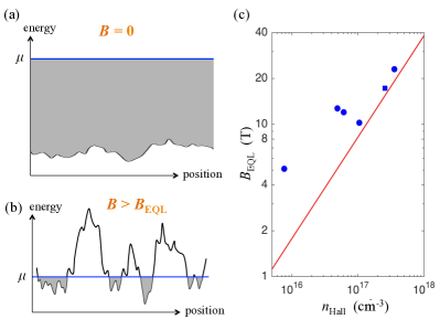
In principle, this puddled state at large corresponds to an insulator, with a finite activation energy for electron transport that is related to the amplitude of the disorder potential. However, owing to the large dielectric response and the relative ease of percolation between wells of the potential in three dimensions, for our samples the expected value of is relatively small, mK),Shklovskii and Efros (1984); Aronzon and Tsidilkovskii (1990); Skinner et al. (2012) below our lowest measurement temperatures. In this sense the picture of electron puddles is not inconsistent with the absence of a sharp upturn in the resistivity at large fields. Clear observation of a magnetic field-driven metal-insulator transition in STO may require lower temperatures or samples with lower electron concentration. It is also possible that impurity positions have some degree of spatial correlation,Merkle and Maier (2003); Szot et al. (2002); Schie et al. (2014) which would further reduce by diminishing the amplitude of disorder potential fluctuations.
Support for the picture of electron puddling at large field can be found by examining the value of the field at which the system enters the EQL. For a spinless, spatially uniform electron gas,
| (4) |
and one can therefore expect to decrease with electron density as . We find, however, that far exceeds this theoretical value for our low-density samples with cm-3, and appears to saturate at a value on the order of T. Indeed, for our lowest-density samples, the disagreement between the observed value of and the prediction of Eq. (4) is larger than times, as shown in Fig. 5(c). It should be emphasized that this disagreement is much larger than the inaccuracy that results from taking the large limit in Eq. (2), which is only when applied to .
This discrepancy between the measured and predicted values of can be explained within the picture of electron puddles, since the typical concentration of electrons within puddles in the EQL is markedly different from the volume-averaged electron concentration . Indeed, in the EQL the typical concentration of electrons within puddles takes a value that is independent of the volume-averaged electron concentrationShklovskii and Efros (1973); Aronzon and Tsidilkovskii (1990):
| (5) |
The value of is determined by statistical fluctuations of the disorder potential over length scales much shorter than the correlation length of the potential. Such fluctuations are driven by the random influence of the many impurity charges, rather than by the weak nonlinear screening from the sparse electrons, and this leads to the independence of on implied by Eq. (5).Shklovskii and Efros (1973); Aronzon and Tsidilkovskii (1990)
For our experiments, Eq. (5) suggests that is on the order of a few times cm-3 in the EQL, while the typical puddle radius is nm. One can then arrive at an estimate for by inserting from Eq. (5) into Eq. (4). This procedure gives , which for our samples is on the order of T. This is consistent with the observed value in samples with small cm-3. At larger values of the doping, the carrier concentration presumably becomes comparable to the total impurity concentration , and the electron gas becomes uniform again so that Eq. (4) is valid.
One can also rationalize the nonlinearity of the - characteristics at within the picture of electron puddles. In particular, an applied electric field facilitates the thermal activation of electrons between adjacent puddles by adding a contribution to the potential energy that varies linearly with the electron position. This picture implies a characteristic electric field scale that is consistent with the observed nonlinearity in the EQL (see SI Sec. V). The nonlinearity is also identical in both the parallel and perpendicular field directions, which is again consistent with the puddle picture (SI Sec. V). Still, the oscillatory behavior of the nonlinearity presented in Fig. 4 remains a prominent puzzle.
Finally, the picture of electron puddles is also qualitatively consistent with the observed linear MR in the EQL, since it corresponds to a landscape where both the disorder potential and the electron concentration have strong spatial fluctuations with a long correlation length. The observed anisotropy of resistivity is also typical in such situations.Shayegan et al. (1985); Aronzon and Tsidilkovskii (1990) (It should be noted, however, that many scenarios for electron transport in the EQL produce significant anisotropy,Askerov (1994) and therefore the anisotropy by itself cannot generally be used as a strong diagnostic of the electron state.)
In conclusion, this paper has presented a clear experimental demonstration of the EQL in bulk STO across a range of samples. Our experiments probe much more deeply into the EQL than previous studies of STO, and into the regime of small , for which a charge ordering instability has long been predicted to occur for a three-dimensional electron gas. While some of our measurements are consistent with the formation of such a CDW state, including in particular a striking nonlinearity in the - characteristics, it seems unlikely to us that electron-electron interactions alone are sufficient to induce such a state within the regime of our experiments. Nonetheless, it remains an open question whether a field-induced CDW state can result from the combination of electron interactions and structural distortions in the STO lattice. An alternate explanation for our measurements is that the large-field behavior is dominated by puddling of electrons in minima of the disorder potential. The observed saturation of the quantum limiting field is apparently consistent with this picture. It may be worth considering, however, whether CDW physics can coexist with an electron-puddled structure. Future studies may provide important additional insight into the electron state in the EQL, particularly if they can complement our transport measurements with thermodynamic probes like capacitance or tunneling spectroscopy, or with studies of magnetic field-driven structural transitions.
Acknowledgments.
Initial measurements of quantum oscillations in reduced STO samples were carried out at the NHMFL in Los Alamos by AB with J. Singleton and F. Balakirev. We are grateful to C. Leighton, P. B. Littlewood, A. Lopez-Bezanilla, B. I. Shklovskii, and K. V. Reich for helpful discussions. AB acknowledges the support of the U.S. Department of Energy (DOE), Office of Science, Basic Energy Sciences (BES), Materials Sciences and Engineering Division. The use of facilities at the Center for Nanoscale Materials, was supported by the U.S. DOE, BES under contract No. DE-AC02-06CH11357. Theory work by BS was initially supported at Argonne National Lab by the U.S. Department of Energy, Office of Science, under contract no. DE-AC02-06CH11357; subsequent theory work was supported as part of the MIT Center for Excitonics, an Energy Frontier Research Center funded by the U.S. Department of Energy, Office of Science, Basic Energy Sciences under Award no. DE-SC0001088. The NHMFL is supported by the NSF Cooperative Agreement No. DMR-1157490 and the State of Florida.
References
- Celli and Mermin (1965) V. Celli and N. David Mermin, “Ground State of an Electron Gas in a Magnetic Field,” Physical Review 140, A839–A853 (1965).
- Kaplan and Glasser (1972) J. I. Kaplan and M. L. Glasser, “Electron Gas in Superstrong Magnetic Fields: Wigner Transition,” Physical Review Letters 28, 1077–1079 (1972).
- Kleppmann and Elliott (1975) W. G. Kleppmann and R. J. Elliott, “The Wigner transition in a magnetic field,” Journal of Physics C: Solid State Physics 8, 2729 (1975).
- Halperin (1987) Bertrand I. Halperin, “Possible States for a Three-Dimensional Electron Gas in a Strong Magnetic Field,” Japanese Journal of Applied Physics 26S3, 1913–1919 (1987).
- Lai (2001) Dong Lai, “Matter in strong magnetic fields,” Reviews of Modern Physics 73, 629–662 (2001).
- Haeni et al. (2004) J. H. Haeni, P. Irvin, W. Chang, R. Uecker, P. Reiche, Y. L. Li, S. Choudhury, W. Tian, M. E. Hawley, B. Craigo, A. K. Tagantsev, X. Q. Pan, S. K. Streiffer, L. Q. Chen, S. W. Kirchoefer, J. Levy, and D. G. Schlom, “Room-temperature ferroelectricity in strained SrTiO3,” Nature 430, 758–761 (2004).
- Ohtomo and Hwang (2004) A. Ohtomo and H. Y. Hwang, “A high-mobility electron gas at the LaAlO3/SrTiO3 heterointerface,” Nature 427, 423–426 (2004).
- Thiel et al. (2006) S. Thiel, G. Hammerl, A. Schmehl, C. W. Schneider, and J. Mannhart, “Tunable Quasi-Two-Dimensional Electron Gases in Oxide Heterostructures,” Science 313, 1942–1945 (2006).
- Caviglia et al. (2008) A. D. Caviglia, S. Gariglio, N. Reyren, D. Jaccard, T. Schneider, M. Gabay, S. Thiel, G. Hammerl, J. Mannhart, and J.-M. Triscone, “Electric field control of the LaAlO3/SrTiO3 interface ground state,” Nature 456, 624–627 (2008).
- Son et al. (2010) Junwoo Son, Pouya Moetakef, Bharat Jalan, Oliver Bierwagen, Nicholas J. Wright, Roman Engel-Herbert, and Susanne Stemmer, “Epitaxial SrTiO3 films with electron mobilities exceeding ,” Nature Materials 9, 482–484 (2010).
- Cowley (1964) R. A. Cowley, “Lattice Dynamics and Phase Transitions of Strontium Titanate,” Physical Review 134, A981–A997 (1964).
- Barrett (1952) John H. Barrett, “Dielectric Constant in Perovskite Type Crystals,” Physical Review 86, 118–120 (1952).
- Frederikse et al. (1967) H. P. R. Frederikse, W. R. Hosler, W. R. Thurber, J. Babiskin, and P. G. Siebenmann, “Shubnikov-de Haas Effect in SrTiO3,” Physical Review 158, 775–778 (1967).
- Yamada and Shirane (1969) Yasusada Yamada and Gen Shirane, “Neutron Scattering and Nature of the Soft Optical Phonon in SrTiO,” Journal of the Physical Society of Japan 26, 396–403 (1969).
- Neville et al. (1972) R. C. Neville, B. Hoeneisen, and C. A. Mead, “Permittivity of Strontium Titanate,” Journal of Applied Physics 43, 2124–2131 (1972).
- Kahn and Leyendecker (1964) A. H. Kahn and A. J. Leyendecker, “Electronic Energy Bands in Strontium Titanate,” Physical Review 135, A1321–A1325 (1964).
- Schooley et al. (1964) J. F. Schooley, W. R. Hosler, and Marvin L. Cohen, “Superconductivity in Semiconducting SrTiO3,” Physical Review Letters 12, 474–475 (1964).
- Mott (1968) N. F. Mott, “Metal-Insulator Transition,” Reviews of Modern Physics 40, 677–683 (1968).
- Zeitler et al. (1994) U Zeitler, A G M Jansen, P Wyder, and S S Murzin, “Magneto-quantum oscillations in the hall constant of three-dimensional metallic semiconductors,” Journal of Physics: Condensed Matter 6, 4289 (1994).
- Murzin et al. (2000) S. S. Murzin, A. G. M. Jansen, and E. G. Haanappel, “Quasi-one-dimensional transport in the extreme quantum limit of heavily doped n-InSb,” Physical Review B 62, 16645–16652 (2000).
- Shayegan et al. (1988) M. Shayegan, V. J. Goldman, and H. D. Drew, “Magnetic-field-induced localization in narrow-gap semiconductors Hg1-xCdxTe and InSb,” Physical Review B 38, 5585–5602 (1988).
- Mani (1989) Ramesh G. Mani, “Possibility of a metal-insulator transition at the Mott critical field in InSb and Hg1-xCdxTe,” Physical Review B 40, 8091–8094 (1989).
- Kozuka et al. (2008) Y. Kozuka, T. Susaki, and H. Y. Hwang, “Vanishing hall coefficient in the extreme quantum limit in photocarrier-doped SrTiO3,” Physical Review Letters 101, 096601 (2008).
- Allen et al. (2013) S. James Allen, Bharat Jalan, SungBin Lee, Daniel G. Ouellette, Guru Khalsa, Jan Jaroszynski, Susanne Stemmer, and Allan H. MacDonald, “Conduction-band edge and Shubnikov-de Haas effect in low-electron-density SrTiO3,” Physical Review B 88, 045114 (2013).
- Lin et al. (2013) Xiao Lin, Zengwei Zhu, Benoît Fauqué, and Kamran Behnia, “Fermi Surface of the Most Dilute Superconductor,” Physical Review X 3, 021002 (2013).
- (26) Crys Tec Gmbh, Köpenicker Str. D-12555 Berlin, Germany. http://www.crystec.de/crystec-d.html .
- Note (1) This commercial product is described in this paper in order to specify adequately the experimental procedure. In no case does such identification imply recommendation or endorsement by the National Institute of Standards and Technology, nor does it imply that it is necessarily the best available for the purpose.
- De Souza et al. (2012) Roger A. De Souza, Veronika Metlenko, Daesung Park, and Thomas E. Weirich, “Behavior of oxygen vacancies in single-crystal SrTiO3: Equilibrium distribution and diffusion kinetics,” Physical Review B 85, 174109 (2012).
- Paladino (1965) A. E. Paladino, “Oxidation Kinetics of Single-Crystal SrTiO3,” Journal of the American Ceramic Society 48, 476–478 (1965).
- Note (2) In principle, a single oxygen vacancy acts stoichiometrically as a double-donor, but it is generally accepted that one of the two electron states remains tightly bound to the doubly-charged oxygen ion, so that the vacancy donates only a single electron to the conduction band.Janotti et al. (2014).
- Ensign and Stokowski (1970) T. C. Ensign and S. E. Stokowski, “Shared Holes Trapped by Charge Defects in ,” Physical Review B 1, 2799–2810 (1970).
- Morin and Oliver (1973) F. J. Morin and J. R. Oliver, “Energy Levels of Iron and Aluminum in ,” Physical Review B 8, 5847–5854 (1973).
- Abrikosov, Alexei A (1988) Abrikosov, Alexei A, Fundamentals of the Theory of Metals (Elsevier, New York, 1988).
- Lin et al. (2015) Xiao Lin, Benoît Fauqué, and Kamran Behnia, “Scalable T2 resistivity in a small single-component fermi surface,” Science 349, 945–948 (2015).
- Note (3) One can note that Eq. (2) assumes that Landau levels are not spin-degenerate. The agreement of this equation with our measurements suggests that this is indeed the case in our samples for all appreciable magnetic fields. This non-degeneracy can be expected if one assumes that the electron -factor in STO is of order unity. In this case the Zeeman energy is of order \tmspace+.1667emeV per Tesla of field, while the Fermi energy in our samples is in the range \tmspace+.1667emeV to \tmspace+.1667emeV, so that the conduction electrons become completely spin polarized even at relatively high Landau levels.
- Murzin (2000) Sergei S. Murzin, “Electron transport in the extreme quantum limit in applied magnetic field,” Physics-Uspekhi 43, 349 (2000).
- Song et al. (2015) Justin C. W. Song, Gil Refael, and Patrick A. Lee, “Linear magnetoresistance in metals: Guiding center diffusion in a smooth random potential,” Physical Review B 92, 180204 (2015).
- Dykhne (1971) A. M. Dykhne, “Anomalous Plasma Resistance in a Strong Magnetic Field,” Soviet Journal of Experimental and Theoretical Physics 32, 348 (1971).
- Parish and Littlewood (2005) Meera M. Parish and Peter B. Littlewood, “Classical magnetotransport of inhomogeneous conductors,” Physical Review B 72, 094417 (2005).
- Kozlova et al. (2012) N. V. Kozlova, N. Mori, O. Makarovsky, L. Eaves, Q. D. Zhuang, A. Krier, and A. Patanè, “Linear magnetoresistance due to multiple-electron scattering by low-mobility islands in an inhomogeneous conductor,” Nature Communications 3, 1097 (2012).
- Khalsa and MacDonald (2012) Guru Khalsa and A. H. MacDonald, “Theory of the SrTiO3 surface state two-dimensional electron gas,” Physical Review B 86, 125121 (2012).
- Note (4) This lowest band has a slight anisotropy of the effective mass,Allen et al. (2013) resulting from the tetragonal distortion of the STO lattice at low temperature, so for the sake of making numerical estimates below we take the effective mass to be equal to the geometric mean of the three perpendicular masses, which gives , where is the bare electron mass.
- Fukuyama (1978) H. Fukuyama, “CDW instability of electron gas in a strong magnetic field,” Solid State Communications 26, 783–786 (1978).
- Gerhardts (1980) R. R. Gerhardts, “Magnetic field induced phase transition of a three-dimensional electron gas,” Solid State Communications 36, 397–401 (1980).
- Richard et al. (1987) J. Richard, P. Monceau, and M. Renard, “Nonlinear magnetoresistance and charge-density-wave depinning at liquid-helium temperatures in NbSe3,” Physical Review B 35, 4533–4536 (1987).
- Bauer and Kahlert (1972) G. Bauer and H. Kahlert, “Low-temperature non-ohmic galvanomagnetic effects in degenerate -type inas,” Physical Review B 5, 566–579 (1972).
- Gruner (1983) G. Gruner, “Nonlinear and frequency-dependent transport phenomena in low-dimensional conductors,” Physica D: Nonlinear Phenomena 8, 1–34 (1983).
- Field et al. (1986) Stuart B. Field, D. H. Reich, B. S. Shivaram, T. F. Rosenbaum, D. A. Nelson, and P. B. Littlewood, “Evidence for depinning of a Wigner crystal in Hg-Cd-Te,” Physical Review B 33, 5082–5085 (1986).
- Heinonen and Al-Jishi (1986) Olle Heinonen and Radi A. Al-Jishi, “Electron-phonon interactions and charge-density-wave formations in strong magnetic fields,” Physical Review B 33, 5461–5464 (1986).
- Johannes and Mazin (2008) M. D. Johannes and I. I. Mazin, “Fermi surface nesting and the origin of charge density waves in metals,” Physical Review B 77, 165135 (2008).
- Cowley (1996) R. A. Cowley, “The Phase Transition of Strontium Titanate,” Philosophical Transactions of the Royal Society of London A: Mathematical, Physical and Engineering Sciences 354, 2799–2814 (1996).
- Shklovskii and Efros (1973) B. I. Shklovskii and A. L. Efros, “Localization of electrons in a magnetic field,” Soviet Journal of Experimental and Theoretical Physics 37, 1122 (1973).
- Shklovskii and Efros (1984) B. I. Shklovskii and A. L. Efros, Electronic Properties of Doped Semiconductors (Springer-Verlag, New York, 1984) available from http://www.tpi.umn.edu/shklovskii.
- Aronzon and Tsidilkovskii (1990) B. A. Aronzon and I. M. Tsidilkovskii, “Magnetic-Field-Induced Localization of Electrons in Fluctuation Potential Wells of Impurities,” Physica Status Solidi (b) 157, 17–59 (1990).
- Skinner et al. (2012) Brian Skinner, Tianran Chen, and B. I. Shklovskii, “Why Is the Bulk Resistivity of Topological Insulators So Small?” Physical Review Letters 109, 176801 (2012).
- Merkle and Maier (2003) Rotraut Merkle and Joachim Maier, “Defect association in acceptor-doped SrTiO3: case study for Fe$́{}_{\mathrm{Ti}}$V$̈{}_{\mathrm{O}}$ and Mn´´Tiv$̈{}_{\mathrm{O}}$,” Physical Chemistry Chemical Physics 5, 2297–2303 (2003).
- Szot et al. (2002) K. Szot, W. Speier, R. Carius, U. Zastrow, and W. Beyer, “Localized Metallic Conductivity and Self-Healing during Thermal Reduction of ,” Physical Review Letters 88, 075508 (2002).
- Schie et al. (2014) Marcel Schie, Rainer Waser, and Roger A. De Souza, “A Simulation Study of Oxygen-Vacancy Behavior in Strontium Titanate: Beyond Nearest-Neighbor Interactions,” The Journal of Physical Chemistry C 118, 15185–15192 (2014).
- Shayegan et al. (1985) M. Shayegan, V. J. Goldman, H. D. Drew, D. A. Nelson, and P. M. Tedrow, “Magnetic-field-induced localization in InSb and ,” Physical Review B 32, 6952–6955 (1985).
- Askerov (1994) Bahram M Askerov, Electron transport phenomena in semiconductors, Vol. 394 (World Scientific, 1994).
- Janotti et al. (2014) Anderson Janotti, Joel B. Varley, Minseok Choi, and Chris G. Van de Walle, “Vacancies and small polarons in ,” Physical Review B 90, 085202 (2014).
Supplementary Information for “Spatially inhomogeneous electron state deep in the extreme quantum limit of strontium titanate”
I Sample preparation and measurement setup
Sample Preparation: As mentioned in the main text, the SrTiO3 single crystals studied here were obtained from Crys Tec GmbH.cry On one side the samples were atomically smooth with regular unit cell high terraces, while the opposite face was unpolished. The (002) peak in all samples in this study had rocking curve full width at half maxima in the range . The samples were first cleaned with solvents (including trichloroethylene) to remove any residue or particulate and were then mounted on a stainless steel sample holder. All annealing was carried out using a SiC radiative heater. The samples were annealed in a prep chamber at C for approximately 30 min to get rid of any adsorbed water or solvents on the holder and substrate. After the pressure of the prep chamber dropped below Pa ( Torr), the sample was cooled down and inserted into the main vacuum chamber, which was typically at a base pressure between Pa and Pa ( Torr and Torr). The sample was heated to temperatures between C and C, depending on the doping level desired, at a rate of C/min to C/min. The pressure in the chamber near the end of the annealing process was Pa ( Torr), comprising mostly H2. Samples were held at the annealing temperature for exactly min, after which time the power to the heater was rapidly reduced and then turned off and the sample was allowed to cool, which took approximately min.
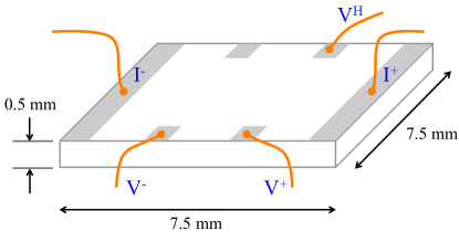
Contacts: The current contacts spanned the full width of the sample ( mm 7.5 mm), while four voltage contact tabs (with dimensions mm mm) were deposited at the edges of the sample (spaced mm apart). NiCr ( nm)/Au ( nm) contacts were sputtered on the unpolished side of the sample after Ar ion milling only the contact pad area for min ( V, mA, incident at ). All samples were typically measured within a week of annealing, as the resistivity was found to increase progressively with time.
Transport Measurements: Simultaneous measurements of the longitudinal and Hall voltages, and , respectively, were carried out in a 5-terminal Hall geometry, as illustrated in Fig. S1. Our measurements used the direct current reversal technique, and the experimental setup was an improved version of the system described in Ref. Suslov, 2010.
Utilized current sources and nanovoltmeters have a built-in option for measurements of differential conductance or differential resistance. Thus, we used the same setup for measurements of differential resistance in the 4-terminal geometry. (Elsewhere in this article, the notation is used in place of .) The differential resistance at a given bias current, , was characterized by measuring changes in voltage, , associated with small excursions in the current, , about the applied bias. During the measurements was swept through a specified range with a finite step size .
Experiments were performed at several magnet/cryostat configurations available at the National High Magnetic Field Laboratory, and the study was performed in magnetic field as high as T and at temperatures ranging from mK to mK using dilution cryostats. Care was taken to ensure that our measurements were not affected by Joule heating.
Contact resistance at low temperatures was too low to be measured reliably ( or lower). Fabrication of contacts with such low resistance was critical for carrying out low-noise voltage measurements at low temperatures, where the samples typically had resistance values in the range to . Furthermore, for measurements in the dilution fridge, the low contact resistances at the current contacts were essential for minimizing heating due to the excitation current.
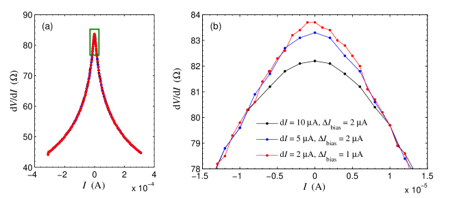
Heating: In order to characterize the effects of the excitation current on heating in the sample, and on the value of the measured resistance in our experiments, we measured for a range of currents between A and A for several values of the current step size and the excitation current . By varying these values at low we were able to substantially vary the power dissipated in a measurement. We observed that for A, the value of was independent of the utilized measurement parameters. This is shown for A, A, and A and A, A and 2A, respectively, in Fig. S2. Our estimations show that at A, current step size A, and excitation current A the power dissipated in the sample was about nW, whereas for A, A, and A this power was about nW. Thus, while corresponding values of the dissipated power differ by more than a factor of , the measurements nonetheless produce the same result for the differential resistance. Therefore, at least at low values of the current bias, the change in measured as a function of bias (Fig. 4 of the main text) is not due to heating. The disagreement at zero bias between the curves for A, A, and A in Fig. S2 can be explained by a coarse graining effect produced by the larger values near the sharp cusp-like feature at zero bias. The data for A is closest to the “intrinsic” curve.
II Zero-field mobility and estimate of impurity concentration
As mentioned in the main text, as-grown STO crystals generally have a relatively large number of impurities that act as deep acceptors.De Souza et al. (2012); Rice et al. (2014) We therefore expect that the concentration of impurities significantly exceeds the concentration of free electrons. Here we show that this expectation is consistent with measurements of the zero-field, low-temperature mobility.
In particular, at low enough temperatures that the mobility saturates at a constant value, one can expect that the electron mobility is limited primarily by scattering from ionized impurities (Rayleigh scattering). For such scattering processes, screening of the impurity potential by conduction electrons is essentially irrelevant in our samples. This can be seen by examining the Thomas-Fermi screening radius
| (S6) |
where is the electron density of states. In our samples nm, which is much longer than the distance between electrons or between charged impurities. (Here, denotes the effective Bohr radius at zero magnetic field.) Consequently, the screening of impurities can be ignored for calculating the scattering cross section. In this case,Dingle (1955)
| (S7) |
Solving Eq. (S7) for gives an estimate of the impurity concentration for a given mobility and carrier density . For the samples presented here, this estimate yields values of of a few times cm-3, which is consistent with our assumptions in the main text and with previous studies.Spinelli et al. (2010); Rice et al. (2014); De Souza et al. (2012)
Of course, this value can be considered an upper-bound estimate for , since the presence of other, short-ranged scatterers will also decrease the mobility. The Coulomb potential created by impurities is also not perfectly described by a constant dielectric function , since the dielectric function is dispersive and thus the dielectric response is not fully developed at short distances from the impurity. Hence, scattering by impurities may be somewhat stronger than implied by Eq. (S7), which would further reduce the estimate for . Theoretical estimates for the dispersive nature of the dielectric function, however, suggest that this effect is not too large for isolated monovalent charges.Reich et al. (2015)
III Hall Resistance
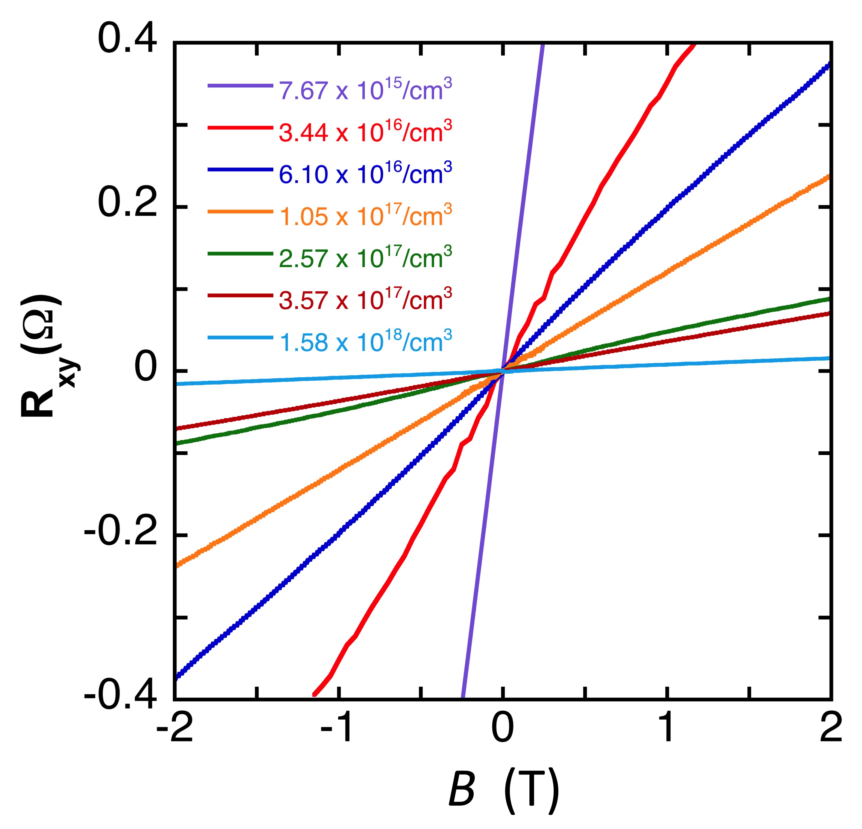
In Fig. S3 we present Hall resistance measurements for the samples studied in this work.
IV Shubnikov-de Haas Analysis
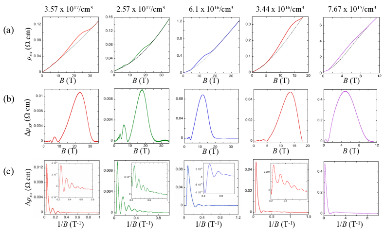
In the main text are presented the results of a Shubnikov-de Haas (SdH) analysis of our doped STO samples. In particular, in this analysis we identify oscillations of the longitudinal resistivity that are periodic in . As mentioned in the main text, this is done by subtracting a smooth, fourth-order polynomial from the curve and identifying the field values corresponding to the maxima of the background-subtracted curve .
In Fig. S4 we show full details of this data analysis procedure for five of our studied samples, each of which is driven into the extreme quantum limit at large field. In particular, for each sample we show the raw curve , the background-subtracted curve , and the same data plotted against the inverse field .
V Nonlinear transport
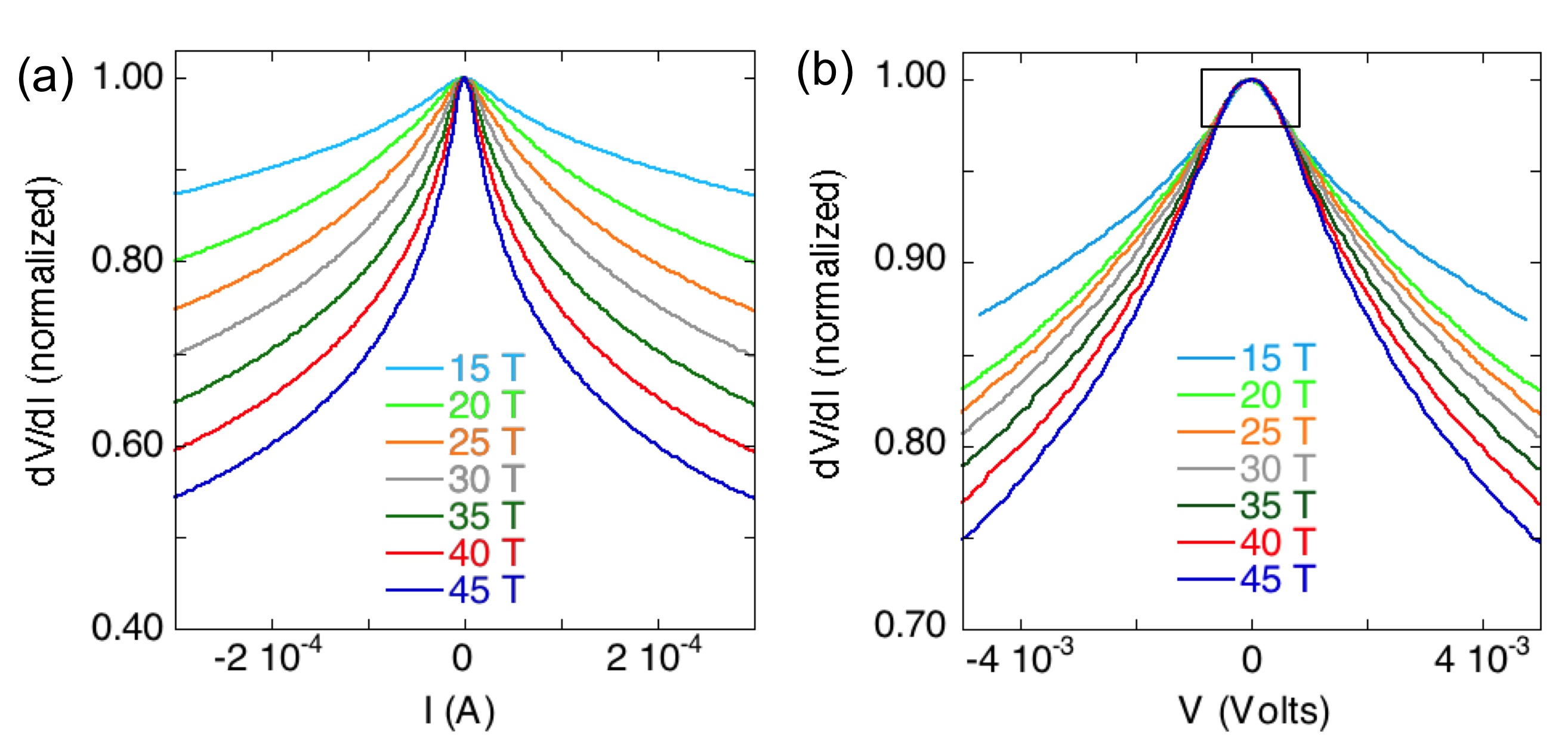
Resistivity Scaling: At high magnetic fields, the resistivity exhibits a significant nonlinearity, such that is a function of both the bias voltage and the magnetic field . We observe that the resistivity can in fact be scaled in such a way that different curves for the differential resistance, , as a function of collapse on top of each other at small . This is shown in Fig. S5(b). The collapse of the curves suggests that one can write , where and are scaling functions.
From the data in Fig. S5 one can extract a characteristic electric field scale for the nonlinearity in multiple different ways. For example, one can define as the value of the electric field above which the scaling shown in Fig. S5(b) is lost. This definition gives mV/cm. Alternatively, one could define as the value for which the differential resistance drops to half its value. Such a definition gives on the order of mV/cm, depending on the value of .
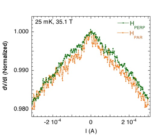
Nonlinearity in the perpendicular versus parallel field directions: Our analysis of the nonlinearity has largely focused on the case where the magnetic field direction is perpendicular to the current direction. Here we briefly show results for the case where the magnetic field and current directions are co-linear. As one can see in Fig. S6, the two cases give essentially identical results for the nonlinear differential resistance.
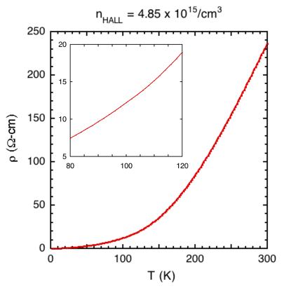
Tetragonal domain walls: At temperatures below K, STO is known to undergo a transition from cubic to tetragonal crystal symmetry.Cowley (1964) Consequently, at K the sample contains domain walls between differently-oriented tetragonal domains, and these can potentially influence the electron transport. (For example, such influence has recently been studied at the STO-LaAlO3 interface.Kalisky et al. (2013); Honig et al. (2013)) These domains are typically tens of microns in size, and the domain walls have a width of about nm and are associated with an electronic energy scale of about meV.Cao and Barsch (1990)
In our experiments, however, we find it unlikely that these domain walls are related to the observed nonlinearity in the electron transport. Most tellingly, the features we observe in the electron transport are strongly magnetic field-dependent, while the domain structure at fixed low temperature is completely insensitive to magnetic field. In addition, we see no sign of any anomalies in the resistivity at K, at which the structural transition occurs. This is shown in Fig. S7.
Nonlinearity in the Electron Puddle Picture: In the picture of “electron puddles” presented in the main text, there is a natural electric field scale for the nonlinearity of the resistivity, which can be derived as follows.
For an almost-completely-compensated semiconductor in the EQL, electrons become localized in wells of the disorder potential with typical radiusAronzon and Tsidilkovskii (1990)
| (S8) |
and typical concentration given by Eq. (4) of the main text. One can estimate the typical distance between puddles by noting that the total number of electrons within a puddle is equal to , and therefore the volume-averaged concentration of electrons is . Rearranging this expression for gives a typical distance between puddles .
In the absence of a bias electric field, the typical activation energy between neighboring puddles is , where is the typical amplitude of the disorder potential [see Eq. (2) of the main text] and is a numerical factor that is typically .Skinner et al. (2012) One can define the typical field scale as the value of the electric field for which the difference in electric potential between puddles due to the applied field becomes equal to the activation energy . In other words, . Rearranging this equation for and substituting gives
| (S9) | ||||
where the second equality is reached by substituting Eqs. (4) and (S8) into Eq. (S9).
For our samples, Eq. (S9) gives mV/cm to mV/cm for between T and T. This range can be compared to the empirical values of , which are between mV/cm and mV/cm.
References
- (1) Crys Tec Gmbh, Köpenicker Str. D-12555 Berlin, Germany. http://www.crystec.de/crystec-d.html .
- Suslov (2010) A. V. Suslov, “Stand alone experimental setup for dc transport measurements,” Review of Scientific Instruments 81, 075111 (2010).
- De Souza et al. (2012) Roger A. De Souza, Veronika Metlenko, Daesung Park, and Thomas E. Weirich, “Behavior of oxygen vacancies in single-crystal SrTiO3: Equilibrium distribution and diffusion kinetics,” Physical Review B 85, 174109 (2012).
- Rice et al. (2014) W. D. Rice, P. Ambwani, M. Bombeck, J. D. Thompson, G. Haugstad, C. Leighton, and S. A. Crooker, “Persistent optically induced magnetism in oxygen-deficient strontium titanate,” Nature Materials 13, 481–487 (2014).
- Dingle (1955) R.B. Dingle, “Scattering of electrons and holes by charged donors and acceptors in semiconductors,” Philosophical Magazine 46, 831–840 (1955).
- Spinelli et al. (2010) A. Spinelli, M. A. Torija, C. Liu, C. Jan, and C. Leighton, “Electronic transport in doped : Conduction mechanisms and potential applications,” Physical Review B 81, 155110 (2010).
- Reich et al. (2015) K. V. Reich, M. Schecter, and B. I. Shklovskii, “Accumulation, inversion, and depletion layers in ,” Physical Review B 91, 115303 (2015).
- Cowley (1964) R. A. Cowley, “Lattice Dynamics and Phase Transitions of Strontium Titanate,” Physical Review 134, A981–A997 (1964).
- Kalisky et al. (2013) Beena Kalisky, Eric M. Spanton, Hilary Noad, John R. Kirtley, Katja C. Nowack, Christopher Bell, Hiroki K. Sato, Masayuki Hosoda, Yanwu Xie, Yasuyuki Hikita, Carsten Woltmann, Georg Pfanzelt, Rainer Jany, Christoph Richter, Harold Y. Hwang, Jochen Mannhart, and Kathryn A. Moler, “Locally enhanced conductivity due to the tetragonal domain structure in LaAlO3/SrTiO3 heterointerfaces,” Nature Materials 12, 1091–1095 (2013).
- Honig et al. (2013) M. Honig, J. A. Sulpizio, J. Drori, A. Joshua, E. Zeldov, and S. Ilani, “Local electrostatic imaging of striped domain order in LaAlO3/SrTiO3,” Nature Materials 12, 1112–1118 (2013).
- Cao and Barsch (1990) Wenwu Cao and Gerhard R. Barsch, “Landau-Ginzburg model of interphase boundaries in improper ferroelastic perovskites of symmetry,” Physical Review B 41, 4334–4348 (1990).
- Aronzon and Tsidilkovskii (1990) B. A. Aronzon and I. M. Tsidilkovskii, “Magnetic-Field-Induced Localization of Electrons in Fluctuation Potential Wells of Impurities,” Physica Status Solidi (b) 157, 17–59 (1990).
- Skinner et al. (2012) Brian Skinner, Tianran Chen, and B. I. Shklovskii, “Why Is the Bulk Resistivity of Topological Insulators So Small?” Physical Review Letters 109, 176801 (2012).