Spin polarized Charge Trapping and Transfer at a HgTe Topological Insulator Quantum Dot
Abstract
This work presents theoretical demonstration of a carrier trap unit formed by dual topological insulator constrictions (TIC) on the HgTe/CdTe quantum well (QW) with inverted band structures. The sample of HgTe/CdTe QW is patterned into a Hall bar device and a topological quantum dot is created by adding split gate electrodes closely on the QW. In sharp contrast to conventional semiconductor quantum dots, the presence or absence of topological edge states in the proposed quantum hall bar system leads to distinct propagating/insulating state of the TICs with large on/off ratio. This topological quantum dot functions as a carrier trap memory element with near perfect program/erase efficiency by proper adjusting the voltages applied to the split gates. For completeness, we also demonstrate that the Rashba spin orbit interaction in the quantum dot does not destroy the topological edge states and have negligible impact on the conductance of the quantum hall bar. The rapid oscillations in conductance can be suppressed when applying a perpendicular magnetic field in the quantum dot.
pacs:
72.25.-b, 71.70.Ej, 42.70.Qs,I INTRODUCTION
Manipulation of the transport properties in topological insulators (TI)Kane ; Fu ; Bernevig1 ; Hasan ; Qi , such as HgTe QWs Bernevig2 ; Yang ; Konig , Hsieh , Xia , and Chen , have attracted rapidly growing interests over the past decadeHsieh2 ; Sonin ; Cheng ; Williams ; Culcer ; Lin ; Lu ; Hong ; Siu ; Bauer ; Mani . In two dimension (2D), a topological insulator is also known as the quantum spin Hall (QSH)insulator, with insulating bulk states and gapless helical edge states. The QSH insulator state was predicted to occur in HgTe QWs with inverted band structureBernevig2 ; Yang and was experimentally demonstrated.Konig These gap-less helical edge states are robust against non-magnetic impurities, crystalline defects, and distortion of the surface, et.al, due to the protection of time-reversal symmetry and non-zero topological invariant.Kane ; Sheng ; Xu ; Wu ; Fu2 These robust helical edge states provide new functional units for the construction of future nano-electronic devices.
The observation of conductance quantization of a nano-scaled constriction in 2DEG, the so-called quantum point contact (QPC), was a hallmark of mesoscopic transport physics.Wees ; Wharam The constriction can be created by etching or adding split gate electrodes on top of the sample. Since then, constrictions in various systems have been studied extensively in various systems. Such constrictions are important building blocks of quantum dots and qubits for many potential device applications e.g., single-electron transistors, quantum computers.Loss ; Imamoglu ; Hanson ; Kastner ; Galindo After the recent discovery of the aforementioned new state of quantum matter, i.e., TI, the topological insulator constrictions in QSH system are of particular interest and offering an elegant way to control the spin and charge transport. Currently, most works focus on the properties of a single TIC under different modulation mechanisms Zhou ; Teo ; Strom ; Krueckl ; Zhang ; Huang ; Klinovaja . It is highly desirable to study the impact of dual/multiple TICs configurations or more complex hybrid structures on the modulation, so as to achieve more functionable electric control of the carrier transport related with the topological helical edge states.
In this work, we investigate theoretically the carrier transport properties in experimentally realizable QSH system. We propose a topological quantum dot formed in between dual TICs in HgTe/CdTe QW with inverted band structure. The TICs are created by proper shaped split gate electrodes on top of the QW. The applied voltages determine the extension of the depletion regions underneath the split gates, making it possible to effectively tune the width of each TIC independently. Rich transmission features will show up with changing the widths of the TICs or the Fermi energy. A minigap can be openned by the finite size effect at TICs, where the edge modes get coupled, results in a conductance dip. This feature enables us to switch on/off the edge channel by changing TIC widths, i.e., tuning the split gate voltages. This configuration of a quantum dot isolated by dual TICs can be used as a basic element in electronic storage devices. Utilizing robust topological edge channels as well as a distinct switch between the QSH edge state and bulk insulator state of TICs, give rise to superior device reliability, endurance, power consumption in the new proposed devices. And bellow context will illustrate these benefits in more detail. We also observed Fano-like or Fabry-Pérot-like resonances arising from the interference in the quantum dot between two TICS. For the additional reference of non-electric modulation, the RSOI modulation considered in this work has a minor influence on the conductance. When applied a perpendicular magnetic field in the quantum dot, more conductance dips come out in the system, and the backscattering process plays a crucial role at high magnetic field regime.
The paper is organized as follows. In Sec. II, we present the theory of electron tunneling through dual TICs structures. In Sec. III, we show the transmission, conductance, charge distribution of QSH bar system according to charge trapping and propagation states to illustrate the role of edge states in electronic storage devices. Finally, we give a brief conclusion in Sec. IV.
II THEORETICAL MODEL
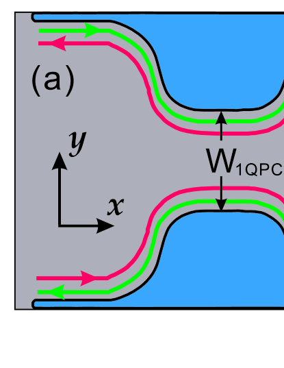
We consider a quantum dot with two TICs formed in a HgTe QSH bar, as shown schematically in Fig. 1(a). Desired inverted band structures of HgTe QW in the low-energy regime are guaranteed by BHZ model, i.e., a four-band Hamiltonian obtained from the eight-band Kane model by neglecting the light-hole and spin-split bands.[] The size confinement of the QW is treated by a hard-wall potential , for and for or , where and denote the lower and upper boundaries of the QSH bar. Allowing the presence of an perpendicular magnetic field, Zeem energy splitting and vector potential are induced. The Landau gauge, = is adopted in our calculation. Finally with including the RSOI, such a single-particle under the modulation of electric potential and magnetic field can be described by a 4 X 4 Hamiltonian in the basis ,
| (1) |
where is the in-plane momentum of electrons, , , , , is the RSOI strength, and and are the parameters describing the band structure of the HgTe/CdTe QW. Note that the QSH state and band insulator state are characterized by the sign of the parameter , which is determined by the thickness of the HgTe/CdTe QW.Bernevig; Konig For negative (positive) M, the QW is in QSH (bulk insulator) state, respectively. For a quasi-one-dimensional (Q1D) QSH bar system shown in Fig. 1(a), the transport property can be obtained by discretizing the Q1D system into a series of transverse strips along the transport direction with sharply narrowed widths at TICs controlled by the split-gate modulation. By means of scattering matrix theory,Zhang2 the transmission amplitude from the m-th input mode to n-th output mode are obtained. We can get the total conductance of the QSH system at zero temperature from the Landauer-Büttiker formula,Buttiker
| (2) |
where the summation is over all propagation modes in the input/output leads which are to the left/right of the quantum dot, is the conductance unit. At a finite temperature T, the ballistic conductance can be written as
| (3) |
where is the Fermi-Dirac distribution.
III RESULTS AND DISCUSSION
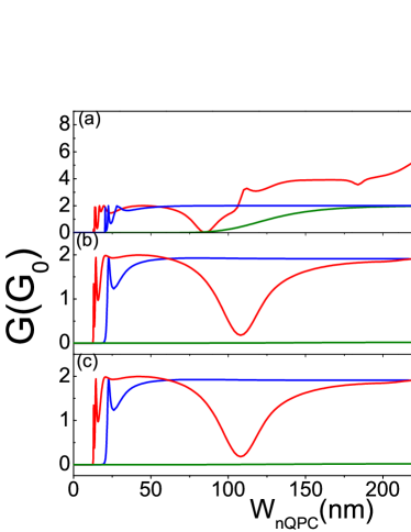
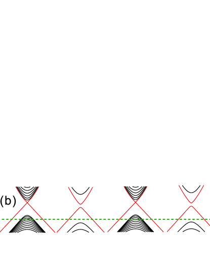
We start by investigating the carrier transport properties in the QSH bar system without RSOI nor magnetic field. Fig. 2 shows the conductance variations with the dual TICs width modulations in three different ways. Due to the finite size effect,Zhang ; Klinovaja a finite gap can be opened in the energy spectra [see Fig. 1(b)] and the gap keeps increasing when reducing the width of TIC. If the Fermi energy locates in this opened energy gap, there is no available propagating mode in the TIC region. Instead, carriers move in evanescent modes that decay rapidly in the TIC region, leading to the suppression of transmission. For extreme narrow TICs, we can always observe vanished conductance as shown in Fig. 2(a) regardless the incident Fermi energy we choose, since the gap is very large. For the green curve, i.e., meV, the Fermi energy is close to the Dirac point of the QSH TI state. Even though only a small gap is opened when the width of TICs is just bellow 100 nm, the Fermi energy has already located in this gap in consistent with the conductance drop. For the blue curve, i.e., meV, the Fermi energy lies far from the Dirac point of the QSH TI state, but still does not touch the edge of subbands (bulk propagating modes) even when TICs are as wide as the leads. Therefore, we need much larger gap in the TICs region with further reduced width to block the edge channel. In the above two cases, only the edge state contributes to the transport and thus the conductance saturates to the value of 2G0 as we relax the TICs. Note that, when the incident energy is fixed to meV, the Fermi level is so apart from the Dirac point that it is able to cross several bulk propagating subbands as the widths of TICs get larger [see Fig. 1(b)]. As we expect, the conductance does not saturate with the width of TICs but exhibits a step-like feature, which corresponds to the opening new bulk propagating modes in TICs regions as they become wider. Furthermore we can observe a dip in conductance curve around nm. The conducting channels come from both the QSH TI edge states and the bulk propagating states, the wave functions of the QSH TI states are squeezed in the central quantum dot region and couple with the bulk states in the narrow TICs. Due to the destructive quantum interference when the charge carriers transmit or reflect at TICs, carriers are localized in the quantum dot without transmission. In Fig. 2(b) and (c) we confirm that each single TIC can effectively block the carrier transport, making our proposed TI quantum dot be possible to work as a electronic storage device as we will discuss in more detail later.
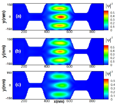
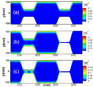
To test the analytical prediction of carrier localization, we plot the density distribution of both topological edge states and bulk states for three cases in Figs. 3(a)-(c), corresponding to the dips in Figs. 2(a)-(c) respectively. The Fermi energy is -15 meV, the widths of dual TICs are as follows, 1) nm, 2) nm, nm, 3) nm, nm. Our calculations demonstrate the localized bound states in the quantum dot. Carriers can be confined in these coupling quantum states with appropriate TICs widths and Fermi energy. Despite the similarity of charge trapping phenomenon as compared to conventional quantum dot, the physical content is different in our system, i.e., the bound states arise from the coupling between the topological edge states and the the bulk states rather than the common quantum confinement due to potential barriers. We can adiabatically change the Fermi energy to approach such condition of charge trapping. It provides the possibility of storing information in these coupling quantum states. However, 1) it is subtle to broke the edge channel by coupling, 2) the transition from trapping phase to transfer phase is rather smooth, and 3) The new mechanism of bound states in the quantum dot does not give rise to some functional benefits. For the purpose of making an electronic storage element, very sharp transition is requested to boost device performance, e.g., quick switch on/off, low standby power, et.al.
To find possible solution, we consider the carrier transport purely in helical edge channels by tuning the Fermi energy to -5 meV. The bulk subband are too far from this Fermi energy to contribute to carrier transport. In the absence of RSOI and magnetic field, we obtain a block diagonal Hamiltonian leading to the time-reversal symmetry for the upper and lower blocks. Therefore we can calculate the carriers transport of spin-up or down state separately. Fig. 4 show the density distribution of the helical edge states in the system for different TICs configurations. For simplicity, we only take the spin-up carriers in to consideration. In Fig. 4(a), the TICs are adequate wide with remained edge channels in whole QSH bar device regions. The carriers propagate along the edge channel and perfectly transport through the topological quantum dot. If the second TIC is blocked as Fig. 4(b). One can see clearly that the carriers from the left incident lead can transport along the top edge into the quantum dot and be reflected to the opposite edge with the same spin orientation due to the helicity of the topological edge states. Then carriers leak out of the quantum dot easily also via the edge channels. Since the width of the first TIC is wide enough, the coupling between top and bottom helical edge stats is very weak. Carriers can transport freely in these edge channels that are well kept in the TICs. If we reduce the width of the first TIC as we did for the second TIC, the coupling between the edge states in the opposite edges become spectacular as we can see in Fig. 4(c). The maximum local probability is approximately 0.17 between the dual TICs which is significantly enlarged comparing to the configuration as shown in Fig. 4(b), in which the maximum local probability is about 0.9]. This gap indicates that the carriers can’t reflect back to left incident lead freely and tend to be stored in the quantum dot. If we keep reducing the width of the TIC, the coupling is strong enough to break the topological edge modes and the first TIC is blocked as well as the second TIC. One can first apply the pinch-off voltage on the split gate to block the second TIC, after the charges are injected from left lead via the spin-polarized helical edge channel, then block the first TIC with the same technique.
In sharp contrast to conventional semiconductor quantum dots, the quantum states in our topological quantum dot are fully spin-polarized helical edge states at a appropriate Fermi energy in the bulk gap (in our discussion, meV). The trapped charges show ringlike density distributions near the boundary as we demonstrated in Fig. 4(c). More importantly, the spin-angular momentum locking, guaranteed by the BHZ hamiltonian, gives rise to spin-polarized charge currents, i.e., the trapped spin-up carriers rotate clockwise and spin-down carriers rotate counterclockwise. Chang If we inject spin polarized currents in to the quantum dot, the polarized spin can be stored as well as the charge in form of persistent spin/charge currents accounting for the topological protected edge states, which are robust against local perturbations. This feature sheds new light on constructing charge/spin trapping memory element for both electronic and spintronic devices.
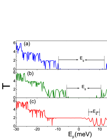
To proceed further, we examine the impact of the HgTe QW thickness, which can be characterized by a band parameter M. As we have discussed, M determines the presence of topological insulator (TI) edge state or only trivial bulk insulator (BI) state. Bernevig2 In Fig. 5, we show the transmission probability as a function of the Fermi energy with different band parameter . The different tunneling precess between BI and TI can be observed when the widths of two TICs are fixed to 100 nm. For BI system, the transmission vanishes when the incident Fermi energy located in the gap of the TICs due to the absence of propagating modes. For higher Fermi energy, transmission plateaus appear as well as many oscillations. Each plateau corresponds to a bulk subband in the TICs. The oscillations originate from the Fabry-Pérot interference between the transmitted and reflected electrons in the quantum dot. For TI system, the resonances are observed even when the Fermi energy is located in the small TI edge gap. When the incident Fermi energy located at a value in the bulk gap but not in the edge gap of the TICs, the transmission is nearly perfect accounting for the helical edge channels. The oscillation of the transmission is smeared out since the backscattering process is suppressed, i.e., few Fabry-Pérot mode are formed. This observation provides us additional way to controlling the carrier transport properties in the proposed HgTe QSH bar device.
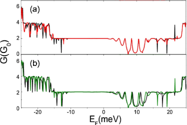
So far, we have studied the carrier transport through proposed QSH bar system exclusively under the electric modulations. For completeness, we further investigate the carrier transport through the HgTe QSH bar in the presence of RSOI or magnetic filed in the quantum dot. Fig. 6(a) shows the conductance as a function of the incident Fermi energy in the presence/absence of RSOI. Since the topological edge states are immune to perturbation of RSOI, the conductance curves of different RSOI strength and meV are almost the same in the energy region meV meV. The conducting channels only come from topological edge states. If the Fermi energy locates out of the bulk band gap, i.e., meV or meV, the bulk modes are opened in the quantum dot. The RSOI would induce a spin splitting of the bulk subbands, resulting in different Fermi wave vectors () for spin-up and spin-down carriers. However the spin splitting is quite small, so one can expect that this spin splitting only leads to slight different behaviors comparing to the case without RSOI in the QD, which is clearly reflected in Fig. 6(a). Finally, we consider an external magnetic field applied perpendicularly to the HgTe quantum dot. Fig. 6(b) shows the conductance as a function of the incident Fermi energy for T and T . Interestingly, we find that the positions of resonance conductance peaks are obviously shifted in a finite magnetic filed of T. Because the magnetic field breaks the time-reversal symmetry and shifts the Dirac point in the energy spectra. Chang Beyond the energy range with only topological edge state, the conductance behaviors are completely different when we apply a finite magnetic field (). More oscillations and sharp dips are observed in our calculation. These dips indicate strong backscattering in the quantum dot. It can be understood by the semiclassical picture: The magnetic field can bend the trajectory of the carriers in favor of cyclotron motion. Charge carriers have more chance to meet with each other before transmit through the quantum dot. Therefore it will enhance the interference between different modes in the quantum dot. If the magnetic field is very large, cyclotron orbit radius is smaller than the size of the quantum dot. The conductance can be fully suppressed. For small RSOI and magnetic field as we employed in above simulation, the topological edge states are well preserved. All the aforementioned features needed to make a spin-polarized charge trapping device element are kept in the proposed quantum dot even in presence of small RSOI and/or magnetic field.
IV CONCLUSIONS
In summary, we have theoretically investigated the carrier transport through a topological quantum dot formed by dual TICs in HgTe QWs with inverted band structures. The conductance of the system can be tuned by changing the width of the TICs or the Fermi energy. we find that the transmission of carriers can be nearly perfect through the system even when Fermi energy is located in both the edge and bulk gap, which would not happen in BI system. The transmission exhibits a series of Fano resonances originating from the Fabry-Pérot modes localized in the quantum dot between dual TICs by adjusting the Fermi energy . with certain TICs configurations and proper incident Fermi energies, carriers can be trapped in the quantum dot in two different forms: 1) in the bulk bound states, 2) in the helical edge states. Espatially for the second case, it may pave a new path of constructing charge/spin trapping memory element for both electronic and spintronic devices. Finally we demonstrate that the proposed topological quantum dot memory element is immune to small RSOI or magnetic filed, as well as some other local perturbations.
References
- (1) C. L. Kane and E. J. Mele, Phys. Rev. Lett. 95, 146802 (2005); 95, 226801 (2005);
- (2) L. Fu, C. L. Kane, and E. J. Mele, Phys. Rev. Lett. 98, 106803 (2007).
- (3) B. A. Bernevig and S. C. Zhang, Phys. Rev. Lett. 96, 106802 (2006).
- (4) M. Z. Hasan and C. L. Kane, Rev. Mod. Phys. 82, 3045 (2010).
- (5) X. L. Qi and S. C. Zhang, Rev. Mod. Phys. 83, 1057 (2011).
- (6) B. A. Bernevig, T. Hughes, and S. C. Zhang, Science 314, 1757 (2006).
- (7) M. König, S. Wiedmann, C. Brüne, A. Roth, H. Buhmann, L. W. Molenkamp, X. L. Qi, and S. C. Zhang, Science 318, 766 (2007).
- (8) W. Yang, K. Chang and S. C. Zhang, Phys. Rev. Lett. 100, 056602 (2008).
- (9) D. Hsieh, D. Qian, L. Wray, Y. Xia, Y. S. Hor, R. J. Cava, and M. Z. Hasan, Nature 452, 970 (2008).
- (10) Y. Xia, D. Qian, D. Hsieh, L. Wray, A. Pal, H. Lin, A. Bansil, D. Grauer, Y. S. Hor, R. J. Cava, and M. Z. Hasan, Nature Phys. 5, 398 (2009).
- (11) Y. L. Chen, J. G. Analytis, J. H. Chu, Z. K. Liu, S.-K. Mo, X. L. Qi, H. J. Zhang, D. H. Lu, X. Dai, Z. Fang, S. C. Zhang, I. R. Fisher, Z. Hussain, and Z. X. Shen, Science 325, 178 (2009).
- (12) D. Hsieh, Y. Xia, D. Qian, L. Wray, J. H. Dil, F. Meier, J. Osterwalder, L. Patthey, J. G. Checkelsky, N. P. Ong, A. V. Fedorov, H. Lin, A. Bansil, D. Grauer, Y. S. Hor, R. J. Cava, and M. Z. Hasan, Nature 460, 1101 (2009).
- (13) E. B. Sonin, Phys. Rev. B 82, 113307 (2010).
- (14) M. Cheng, Phys. Rev. B 86, 195126 (2012).
- (15) J. R. Williams, A. J. Bestwick, P. Gallagher, Seung Sae Hong, Y. Cui, Andrew S. Bleich, J. G. Analytis, I. R. Fisher, and D. G. Gordon, Phys. Rev. Lett. 109, 2056803 (2012).
- (16) D. Culcer, PHYSICA E 44, 860 (2012).
- (17) L. Z. Lin, F. Cheng, L. B. Zhang, D. Zhang, and W. Yang, Phys. Rev. B 87, 245311 (2013).
- (18) H. Lu, A. Zhao, and S. Shen, Phys. Rev. Lett. 111, 146802 (2013).
- (19) S. Hong, Y. Zhang, J. Cha, X. Qi, and Y. Cui, Nano Lett. 14, 2815 (2014).
- (20) Z. Siu, M. Jalil, and S. Tan, Scientific Reports 4, 5062 (2014).
- (21) S. Bauer, and C. Bobisch, Nature Communications 7, 11381 (2016).
- (22) A. Mani, C. Benjamin, Phys. Rev. Appl. 6 014003 (2016)
- (23) D. N. Sheng, Z. Y. Weng, L. Sheng, and F. D. M. Haldane, Phys.Rev. Lett. 97, 036808 (2006).
- (24) C. Xu and J. E. Moore, Phys. Rev. B 73, 045322 (2006).
- (25) C. J. Wu, B. A. Bernevig, and S. C. Zhang, Phys. Rev. Lett. 96, 106401 (2006).
- (26) L. Fu and C. L. Kane, Phys. Rev. B 76, 045302 (2007).
- (27) B. J. van Wees, H. van Houten, C. W. J. Beenakker, J. G. Williamson, L. P. Kouwenhoven, D. van der Marel, and C. T. Foxon, Phys. Rev. Lett. 60, 848 (1988).
- (28) D. A. Wharam, T. J. Thornton, R. Newbury, M. Pepper, H. Ahmed, J. E. F. Frost, D. G. Hasko, D. C. Peacock, D. A. Ritchie, and G. A. C. Jones, J. Phys. C 21, 209 (1988).
- (29) Daniel Loss and David P. DiVincenzo, Phys. Rev. A 57, 120 (1998).
- (30) A. Imamoglu, D. D. Awschalom, G. Burkard, D. P. DiVincenzo, D. Loss, M. Sherwin, and A. Small, Phys. Rev. Lett. 83, 4204 (1999).
- (31) R. Hanson, L. P. Kouwenhoven, J. R. Petta, S. Tarucha, and L. M. K. Vandersypen, Rev. Mod. Phys. 79, 1217 (2007).
- (32) M. A. Kastner, Rev. Mod. Phys. 64, 849 (1992).
- (33) A. Galindo and M. A. M. Delgado, Rev. Mod. Phys. 74, 347 (2002).
- (34) K. Chang and W. Lou, Phys. Rev. Lett. 106, 206802 (2011).
- (35) B. Zhou, H. Lu, R. Chu, S. Shen, and Q. Niu, Phys. Rev. Lett. 101, 246807 (2008).
- (36) J. C. Y. Teo and C. L. Kane, Phys. Rev. B 79, 235321 (2009).
- (37) A. Strom and H. Johannesson, Phys. Rev. Lett. 102, 096806(2009).
- (38) V. Krueckl and K. Richter, Phys. Rev. Lett. 107, 086803 (2011).
- (39) C. W. Huang, S. T. Carr, D. Gutman, E. Shimshoni, and A. D. Mirlin, Phys. Rev. B 88, 125134 (2013).
- (40) L. B. Zhang, F. Cheng, F. Zhai, and K. Chang, Phys. Rev. B 83, 081402(R) (2011).
- (41) J. Klinovaja and D. Loss, Phys. Rev. B 92, 121410(R) (2015).
- (42) L. Zhang, P. Brusheim, and H. Q. Xu, Phys. Rev. B 72, 045347 (2005).
- (43) M. Buttiker, Y. Imry, R. Landauer, adn S. Pinhas, Phys. Rev. B 31, 6207 (1985).