Room-temperature formation of Pt3Si/Pt2Si films on poly-Si substrates
Abstract
We propose a way of formation of thin bilayer Pt3Si/Pt2Si films at room temperature on poly-Si substrates by Pt magnetron sputtering and wet etching, obtain such film, investigate its structure and phase composition and estimate the thickness of its layers. We verify by direct x-ray photoelectron-spectroscopic measurements our previous observation of the Pt2Si layer formaton between Pt and poly-Si films as a result of Pt magnetron sputtering at room temperature. This layer likely appears due to high enough temperature of Pt ions in the magnetron plasma sufficient for chemical reaction of the silicide film formation on the Si surface. The Pt3Si layer likely forms from the Pt–Pt3Si layer (Pt95Si5), which arises under Pt film during the magnetron sputtering, as a result of Pt removal by wet etching.
Platinum silicides have attracted attention of researchers for a number of decades due to their exceptional prospectiveness in microelectronics and silicon-based microphotonics.Samsonov, Dvorina, and Rud’ (1979); Murarka (1983); *Murarka-1995 PtSi infrared detector arrays represented a qualitative breakthrough and opened a new era in the infrared imaging technology.Rogalski (2012); *Kimata_2-PtSi Now Pt silicides are considered as metals for Schottky-barrier formation to poly-Si:P in thin-film diode bolometers.Yuryev et al. (2015a, b) There is no doubt about the prospectiveness of their application as ohmic contacts and submicron lines in microelectronics especially taking into account their low formation temperatures that is very important for CMOS and especially for nanoelectronic devices.Xu et al. (1996); *Silicides_ohmic_contacts; *VCIAN2011 In addition, low-temperature silicides, e.g. Pt2Si, are expected to be suitable for formation of uniform Schottky contacts in devices of power electronics in which the sizes of contacts reach millimeters and nonuniformity of the barrier height causes a significant increase in reverse current.Komarov et al. (2011) Pt silicide ohmic contacts as well as Schottky barrier formation on polycrystallineColgan, Gambino, and Hong (1996) or amorphous silicon is of special interest for photovoltaic and sensor technology.Yuryev et al. (2015b) So, this class of materials should be considered as one of the most friendly ones to silicon technology. However, as the used silicide films become thinner and reach tens or even units of nanometers their resistivity becomes of primary importance. In this connection Pt3Si, which has the lowest sheet resistance among the Pt silicides (18.9 in comparison with 2.6 of Pt, 31.8 of Pt2Si and 57.6 of PtSi),Streller et al. (2016) starts to play the main role. So, the development of simple processes of formation of thin Pt3Si films becomes more and more important.
This letter presents a simple CMOS compatible process of a thin bilayer Pt3Si/Pt2Si film formation at room temperature on a polycrystalline silicon substrate.
A 35-nm thick film of platinum was deposited by magnetron sputtering at room temperature on a 125-nm thick poly-Si:P layer formed on a Si3N4/SiO2/Si(001) artificial substrate (Fig. 1). After deposition, platinum was removed by chemical etching in a warm aqueous solution of aqua regia (H2O : HCl : HNO3 [4 : 3 : 1]).111 The reaction is 3Pt + 18HCl + 4HNO 3H2[PtCl6] + 4NO + 8H2O. Details of the sample preparation process can be found in Ref. Yuryev et al., 2015a.
The samples were studied by means of the X-ray photoelectron spectroscopy (XPS). The measurements were carried out using a cylindrical mirror electron energy analyserHafner, Arol Simpson, and Kuyatt (1968) (Riber EA 150) installed in the ultrahigh-vacuum chamber; the residual gas pressure in the chamber did not exceed Pa. Non-monochromatic Al Kα x-rays ( eV) were used for photoexcitation of electrons. Survey spectra were scanned at the resolution (FWHM) better than 1.8 eV; high resolution spectra of specific elements were obtained at the resolution not worse than 0.96 eV. XPSPEAK 4.1 peak fitting program was utilized for treatment of spectra. It was taken into the account during peak deconvolution that the Al Kα band consists of two lines, K and K, with energy difference of eV. Shifts of peaks related to elements in chemical compounds were compared with the NIST X-ray Photoelectron Spectroscopy (XPS) Database.Lee et al. (2002); Naumkin et al. (2012) Relative concentrations of atoms were estimated from ratios of normalized areas under corresponding peaks. Inelastic mean free path (IMFP) was estimated using TPP-2M equation and the NIST Database.Powell and Jablonsky (2010a, b) The spectrometer was calibrated against the Si4+ signal ( eV) since the C 1 XPS peak recorded at high resolution had low signal-to-noise ratio (Fig. 2) that did not allow us to obtain reliable data on its energy position.
The scanning transmission electron microscopy (STEM) image was obtained using the Carl Zeiss Libra-200 FE HR transmission electron microscope; the WSxM software was used for image processing.Horcas et al. (2007)
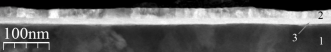
Fig. 1 demonstrates a STEM image of the as-deposited Pt/poly-Si structure. This structures was previously analysed in details using STEM, x-ray diffraction and reflection, and XPS. It is composed by a poly-Si layer, a layer of Pt and an interfacial layer consisting of a Pt95Si5 layer formed on a layer of Pt2Si.Yuryev et al. (2015a) This structure was subjected to wet etching to remove Pt.
Photoelectron peaks of Pt, Si, O and C are observed in the survey photoelectron spectrum of the film obtained after Pt removal (Fig. 2). Monotonic growth of signal is observed in the spectrum on the right (at the higher side) of the Pt 4 doublet that is explained by inelastic scattering of the photoexcited 4 electrons of Pt. This allows us to make a conclusion that the film containing Pt is overlaid by a layer of another composition in which the inelastic scattering happens.Tougaard (1996)
A high-resolution photoelectron spectrum of Pt 4 consists of three components (Fig. 3a). The first one is described by a doublet with eV and distance between peaks eV which may be attributed to Pt3Si; the next one with eV and eV obviously corresponds to Pt2Si.Naumkin et al. (2012); Streller et al. (2014, 2015); Fryer and Lad (2016) The third component lays at higher energies ( eV, eV) and may be attributed to both platinum oxide PtOx ( to 74.6 eV)222 Likely PtO, eV, Ref. Naumkin et al., 2012. and PtCl2 ( eV)Naumkin et al. (2012) or [Pt(NH3)2(NO2)2]333 CAS Registry No. 14286023, Ref. Naumkin et al., 2012. ( eV)Naumkin et al. (2012) which may arise as a result of Pt etching in the aqua regia solution. The ratio of peak areas for Pt3Si, Pt2Si and PtOx is .
The main contribution to the signal of silicon (Fig. 3b) is made by Si4+ ( eV) obviously related to silicon dioxide. In addition, a Si3+ peak can be detected by deconvolution which can be explained by superposition of photoelectron peaks related to Pt3Si, Pt2Si ( eV) and SiOx compounds having a broad range of binding energy values ( to 103.6 eV)Naumkin et al. (2012). An estimate of contribution of Si atoms contained in Pt3Si and Pt2Si to this peak made in assumption of uniformity of the upper film and taking into account empirical sensitivity factors of platinum and silicon gives the value of %.
Notice that an additional cycle of etching in the aqua regia solution changed neither a ratio of the photoelectron peak intensities nor their energy positions.

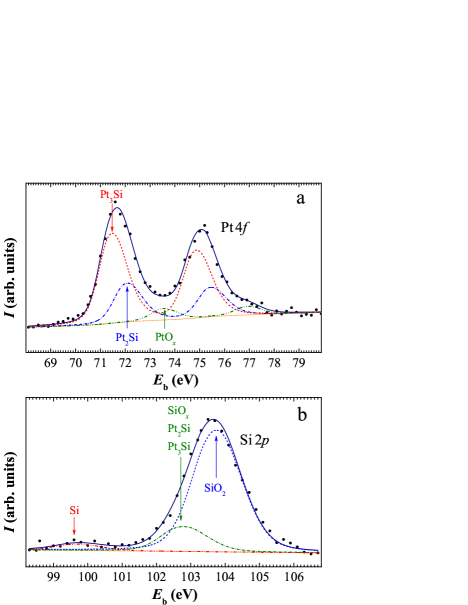
It should be noted also that a small photoelectron peak at eV is also observed in the Si 2 spectrum; it corresponds to pure Si of the polycrystalline substrate that allows us to roughly estimate the thickness of the formed film by 3 to 5 values of inelastic mean free path of electrons, i.e. by the value from 5 to 10 nm.
More accurate estimation of the film thickness can be made from the ratio of areas under the Pt 4 peaks of Pt3Si and Pt2Si . Let us suppose that the Pt3Si layer overlays the Pt2Si one. (This assumption is based on the x-ray phase analysis according to which the Pt2Si and Pt95Si5 layers, 5.6 and 10 nm thick, respectively, arise between poly-Si and Pt as a result of Pt sputtering.)Yuryev et al. (2015a) Considering the IMFP valuePowell and Jablonsky (2010b) of Pt3Si we obtain the thickness of the Pt3Si layer from the values of densities and molar weights of Pt3Si and Pt2Si, and the thickness of the Pt2Si layer :444 The value of is calculated from a recursive equation: , where is the inelastic mean free path of electrons in Pt3Si,Powell and Jablonsky (2010b) , , and are molar weights and densities of Pt2Si and Pt3Si, respectively. nm. So, the total thickness of the bilayer Pt-silicide film nm that is in good agreement with the above rough estimate.
Now, if we assume that the Pt95Si5 layer previously detectedYuryev et al. (2015a) under Pt is a mixture of Pt and Pt3Si (16Pt + Pt3Si) we may suppose also that Pt is etched away from this layer during processing in the aqua regia solution and the Pt3Si layer is deposited atop Pt2Si. We can estimate from the thickness of Pt95Si5 and the densities of Pt, Pt95Si5 (20.5 g/cm3)Yuryev et al. (2015a) and Pt3Si: nm. Thus, the silicide film thickness estimate of 8.0 nm obtained from the x-ray phase analysisYuryev et al. (2015a) corresponds with that obtained from XPS.
In summary, we can make the following conclusions. (i) We have verified our previous observation of Pt2Si formation in between Pt and poly-Si films as a result of Pt magnetron sputtering at room temperature.Yuryev et al. (2015a) This phenomenon probably occurs due to high enough kinetic energy of Pt ions reaching the Si surface sufficient to give rise to chemical reaction of the silicide film formation. It opens a pathway to room-temperature process of formation of thin Pt silicide films on Si. (ii) We have proposed a way of formation of thin bilayer Pt3Si/Pt2Si films on poly-Si substrates at room temperature by magnetron sputtering of Pt followed by etching in a warm aqueous solution of aqua regia and obtained such films using this completely CMOS compatible process. (iii) Using the x-ray photoelectron spectroscopy we have verified the structure and composition of the formed Pt3Si/Pt2Si films; we have estimated the thickness of the Pt3Si layer of the films and found it to be equal to nm; the thickness of the Pt3Si/Pt2Si films has been found to be nm. The obtained estimates practically coincide with those made on the basis of our previous data of the x-ray phase analysis.Yuryev et al. (2015a) (iv) We assume that the Pt3Si layer is formed from the Pt95Si5 layer, which appears under Pt film during the magnetron sputtering,Yuryev et al. (2015a) as a result of Pt removal by wet etching.
This research was funded by RFBR (grant No. 16-32-00854). Equipment of the Center for Collective Use of Scientific Equipment of GPI RAS was used for the study. We thank Ms. N. V. Kiryanova for her contribution to management of this research, Mr. O. V. Uvarov for obtaining the STEM images and Ms. L. A. Krylova for chemical treatments of the samples.
References
- Samsonov, Dvorina, and Rud’ (1979) G. V. Samsonov, L. A. Dvorina, and B. M. Rud’, Silicides (Metallurgia, Moscow, 1979) in Russian.
- Murarka (1983) S. P. Murarka, Silicides for VLSI Applications (Academic Press, New York, 1983).
- Murarka (1995) S. P. Murarka, Intermetallics 3, 173 (1995).
- Rogalski (2012) A. Rogalski, Opto-Electron. Rev. 20, 279 (2012).
- Kimata (2001) M. Kimata, in Infrared Detectors and Emitters: Materials and Devices, edited by P. Capper and C. T. Elliott (Kluwer Adamic Publishers, Dordrecht, 2001) Chap. 4, pp. 77–98.
- Yuryev et al. (2015a) V. A. Yuryev, K. V. Chizh, V. A. Chapnin, S. A. Mironov, V. P. Dubkov, O. V. Uvarov, V. P. Kalinushkin, V. M. Senkov, O. Y. Nalivaiko, A. G. Novikau, and P. I. Gaiduk, J. Appl. Phys. 117, 204502 (2015a).
- Yuryev et al. (2015b) V. A. Yuryev, K. V. Chizh, V. A. Chapnin, and V. P. Kalinushkin, Proc. SPIE 9519, 95190K (2015b).
- Xu et al. (1996) D.-X. Xu, J. P. McCaffrey, S. R. Das, G. C. Aers, and L. Erickson, Appl. Phys. Lett. 68, 3588 (1996).
- Gambino and Colgan (1998) J. Gambino and E. Colgan, Mater. Chem. Phys. 52, 99 (1998).
- Yuryev and Arapkina (2011) V. A. Yuryev and L. V. Arapkina, Nanoscale Res. Lett. 6, 522 (2011).
- Komarov et al. (2011) F. Komarov, O. Milchanin, T. Kovalyova, J. Solovjov, A. Turtsevich, and C. Karwat, in 9th International Conference “Interaction of Radiation with Solids”, September 20–22, 2011 (Minsk, Belarus, 2011) pp. 365–367.
- Colgan, Gambino, and Hong (1996) E. G. Colgan, J. P. Gambino, and Q. Z. Hong, Mater. Sci. Eng., R 16, 43 (1996).
- Streller et al. (2016) F. Streller, Y. Qi, J. Yang, F. Mangolini, A. M. Rappe, and R. W. Carpick, J. Phys. Chem. Lett. 7, 2573 (2016).
- Note (1) The reaction is 3Pt + 18HCl + 4HNO 3H2[PtCl6] + 4NO + 8H2O.
- Hafner, Arol Simpson, and Kuyatt (1968) H. Hafner, J. Arol Simpson, and C. E. Kuyatt, Rev. Sci. Instrum. 39, 33 (1968).
- Lee et al. (2002) A. Y. Lee, D. M. Blakeslee, C. J. Powell, and J. R. Rumble, Jr., Data Science Journal 1, 1 (2002).
- Naumkin et al. (2012) A. V. Naumkin, A. Kraut-Vass, S. W. Gaarenstroom, and C. J. Powell, NIST X-ray Photoelectron Spectroscopy Database. NIST Standard Reference Database 20, Version 4.1 (National Institute of Standards, Gaithersburg, MD, USA, 2012).
- Powell and Jablonsky (2010a) C. J. Powell and A. Jablonsky, J. Electron Spectrosc. Relat. Phenom. 331, 178 (2010a).
- Powell and Jablonsky (2010b) C. J. Powell and A. Jablonsky, NIST Electron Inelastic-Mean-Free-Path Database. Version 1.2, SRD 71 (National Institute of Standards, Gaithersburg, MD, USA, 2010).
- Horcas et al. (2007) I. Horcas, R. Fernandez, J. M. Gomez-Rodriguez, J. Colchero, J. Gomez-Herrero, and A. M. Baro, Rev. Sci. Instrum. 78, 013705 (2007).
- Tougaard (1996) S. Tougaard, J. Vacuum Sci. Technol. A 14, 1415 (1996).
- Streller et al. (2014) F. Streller, G. E. Wabiszewski, F. Mangolini, G. Feng, and R. W. Carpick, Adv. Mater. Interfaces 1, 1300120 (2014).
- Streller et al. (2015) F. Streller, R. Agarwal, F. Mangolini, and R. W. Carpick, Chem. Mater. 27, 4247 (2015).
- Fryer and Lad (2016) R. T. Fryer and R. J. Lad, J. Alloys Compd. 682, 216 (2016).
- Note (2) Likely PtO, eV, Ref.\tmspace+.1667em\rev@citealpnumNIST_XPS_Database.
- Note (3) CAS Registry No.\tmspace+.1667em14286023, Ref.\tmspace+.1667em\rev@citealpnumNIST_XPS_Database.
- Note (4) The value of is calculated from a recursive equation: , where is the inelastic mean free path of electrons in Pt3Si,Powell and Jablonsky (2010b) , , and are molar weights and densities of Pt2Si and Pt3Si, respectively.