∎
Tunable Electronic Properties of Multilayer Phosphorene and Its Nanoribbons ††thanks: The work was primarily supported by the NSF (DMR-1121288) through the UW-Madison MRSEC seed project. Supplementary funds were provided by the Splinter Professorship in Electrical and Computer Engineering. The work was performed using the resources of the UW-Madison Center for High Throughput Computing (CHTC).
Abstract
We study the effects of a vertical electric field on the electronic band structure and transport in multilayer phosphorene and its nanoribbons. In phosphorene, at a critical value of the vertical electric field (), the band gap closes and the band structure undergoes a massive-to-massless Dirac fermion transition along the armchair direction. This transition is observable in quantum Hall measurements, as the power-law dependence of the Landau-level energy on the magnetic field goes from below , to at , to above . In multilayer phosphorene nanoribbons (PNRs), the vertical electric field can be employed to manipulate the midgap energy bands that are associated with edge states, thereby giving rise to new device functionalities. We propose a dual-edge-gate PNR structure that works as a quantum switch.
Keywords:
Phosphorene Edge states NEGF1 Introduction
Black phosphorus (BP) is a thermodynamically stable allotrope of phosphorus with a layered structure. The layers of covalently bonded atoms are held together by the van der Waals interaction. Similar to obtaining graphene from graphite by mechanical exfoliation, BP can be isolated to a few layers lu2014plasma ; liu91acs . The resulting structure is a recent addition to the family of two-dimensional (2D) materials called multilayer phosphorene. Monolayer phosphorene has a direct band gap of 1.45 eV liu91acs . In multilayer phosphorene, the gap decreases with increasing number of layers owing to relatively strong van der Waals interactions between the layers and remains direct zhang2014extraordinary . This makes phosphorene a promising candidate for electronic and optical applications tran2014layer ; jing2015small ; buscema2014fast ; koenig2014electric ; xia2014rediscovering ; ccakir2015significant ; ccakir2014tuning . Moreover, the phosphorene crystal structure is highly anisotropic, which gives rise to phenomena such as anisotropic electronic and thermal transport fei2014strain ; fei2014enhanced ; xia2014rediscovering ; yuan2015transport ; qin2015anisotropic ; cai2015giant , linear dichroism xia2014rediscovering ; yuan2015transport , and anisotropic plasmons Low2014Plasmons . Additionally, owing to its heavily puckered structure, phosphorene is highly tunable by strain elahi2015modulation ; fei2014strain and electric field fei2014enhanced ; das2014tunable . In particular, applying an electric field normal to the layers reduces the band gap, leading to a transition from a moderate-gap semiconductor to a semimetal kim2015observation . Applying an electric field also leads to the emergence of more exotic features of phosphorene, including nontrivial topological phases dutreix2016laser ; liu2015switching ; low2015topological . However, the transition of the Landau levels (LLs) under the influence of electric field as a trademark of the topological phase transition has not been fully understood. Furthermore, little is known about the possible practical use of electric-field modulation of the electronic characteristics of nanostructures based on phosphorene, such as nanoribbons carvalho2014phosphorene ; Guo2014JPCC ; Ali2015JPhysD ; peng2014edge .
In this paper, we investigate the effects of a vertical electric field on the electronic properties (band structure and electronic transport) of multilayer phosphorene and its nanoribbons. In multilayer phosphorene at low fields, electrons with momenta in the zigzag direction [Fig. 1(a)] have parabolic bands, but in the armchair direction they behave as massive Dirac fermions with a gap-dependent effective mass. At a critical electric field , the gap closes, and electrons exhibit a massive-to-massless Dirac fermion transition. Above , there are two Dirac points, and the band structure is that of anisotropic massless Dirac fermions. This continuous massive-to-massless Dirac fermion transition could be observed in Hall measurements, as the LL energy dependence on the magnetic field would change from linear below , to the novel 2/3-power at , to the square-root dependence above . If two-dimensional (2D) bulk phosphorene is nanostructured in one dimension (1D), the electronic properties of the resulting quasi-1D phosphorene nanoribbon (PNR) will strongly depend on the direction of confinement and the type of edge termination. In particular, metallic multilayer PNRs have twofold-degenerate bands within the bulk gap and the associated wave functions are localized near the ribbon edges. We show that the application of a vertical electric field in metallic PNRs can selectively affect electrons in these midgap bands and thereby give rise to novel functionalities. We propose a dual-edge-gate structure that affects these midgap states and drives the conducting-to-insulating transition in PNRs, thus enabling field-effect transistor action compatible with modern nanoelectronics, and potentially leading to new PNR-based devices.
2 The Tight-Binding Model
The band structure of multilayer phosphorene is described by a tight-binding (TB) Hamiltonian
| (1) |
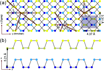
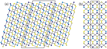
which was parametrized on the basis of first-principles calculation within the approximation rudenko2015toward ; rudenko2014quasiparticle . As the TB parametrization was benchmarked for mono-, bi- and trilayers, we restrict our study here to these three systems, but note that TB may be suitable for larger multilayers, as well. A phosphorene monolayer contains two sublayers in a puckered structure and has four atoms per unit cell. Each additional layer brings four more atoms to the unit cell (see the structure of bilayer phosphorene in Fig. 1), with odd-numbered layers aligned with other odd-numbered ones, and analogously for even-numbered layers. A unit cell for bilayer phosphorene is denoted by the shaded box in Fig. 1(a). In the nearest-neighbor approximation, there are fifteen relevant tight-binding hopping parameters (Table 1), ten intralayer and five interlayer. The multilayer phosphorene structure is highly anisotropic. Cutting phosphorene in the (horizontal) direction (see Fig. 1) would result in an armchair edge, while cutting along the (vertical) direction would result in a zigzag edge. We refer to the -direction as armchair and the -direction as zigzag.
| 1 | 6 | |||||||
|---|---|---|---|---|---|---|---|---|
| 2 | 7 | |||||||
| 3 | 8 | |||||||
| 4 | 9 | |||||||
| 5 | 10 |
3 Bulk Multilayer Phosphorene in a Vertical Electric Field
The band structure of trilayer phosphorene is depicted in Fig. 2(a); note the rectangular Brillouin zone (BZ) and its high-symmetry and points along the and directions. The band gap, , is at the point and has a value of eV. Along the zigzag direction, both the conduction band (CB) and the valence band (VB) show quadratic dependencies on the wave vector [Fig. 2(a)]. We calculate the effective masses of (CB) and (VB), where is the free-electron rest mass. In the armchair direction, however, the dispersion has an asymptotic linear trend. To describe this highly anisotropic band structure near the band gap, we propose a low-energy two-band Hamiltonian as
| (2) |
Here, are the Pauli matrices, and are the effective masses in the zigzag direction, and is the Fermi velocity in the armchair direction. In Fig. 2(b), we see that the fit from this effective two-band Hamiltonian (red dots) agrees very well with the CB and VB dispersions obtained by TB (solid curve) within eV of midgap. Finding the dispersion for from the two-band Hamiltonian (2) leads to
| (3) |
This is a characteristic dispersion of massive relativistic particles weinberg1972gravitation , where plays the role of rest energy. Upon employing the relativistic definition of the effective mass as , we obtain an effective mass for both CB and VB in the armchair direction to be , a value close to the experimentally obtained kim2015observation , which could not be explained previously based on the parabolic approximation. Thus, it is important to consider electrons in the armchair direction as massive Dirac fermions.
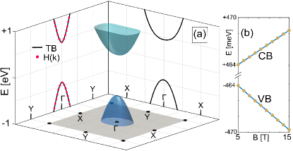
Since unbiased phosphorene is a conventional 2D electron gas, the CB and VB edges are expected to have linear dependencies on an applied vertical magnetic field zhou2015landau ; pereira2015landau ; ghazaryan2015aspects ; the CB/VB edge in a magnetic field is the lowest/highest Landau level (LL) in the CB/VB, respectively. In order to test this hypothesis, magnetic field is incorporated in the tight-binding model through the Peierls substitution, which adds a phase to the hopping term between any two sites,
| (4) |
where is the vector potential and is the magnitude of the magnetic induction in -direction. By this substitution, one will arrive at Harper’s equation Harper1955 ; Thouless1982 ; Wakabayashi1999 ; Wiegeman1984 , and LLs are obtained by numerical calculation of its eigenvalues. For unbiased trilayer phosphorene, the LLs were calculated at various magnetic fields. The CB and VB edges are shown in Fig. 2(b). Predictably, the CB and VB edge change linearly as a function of magnetic flux density . (While our calculations of LLs versus presented throughout this paper hold down to low magnetic fields, LLs are unlikely to be resolved in experiment at low fields owing to disorder ( is needed to resolve LLs, where is the electron mobility in the sample). Therefore, we present the dependence of the lowest Landau levels in the conduction and valence bands on in the experimentally relevant high-magnetic-field range that was previously used by Jiang et al. Jiang2007PRL for the Hall measurement on graphene.)
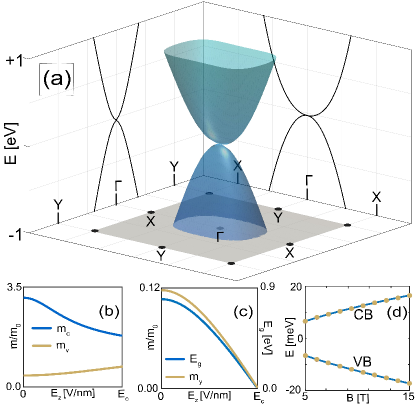
Next, we extend our model to the case of a vertical electric field [applied normal to the layers, i.e., in the -direction in Fig. 1(a)]. In the TB calculations, is accounted for by assuming a linear potential drop across the structure extending from to ( is the thickness): a potential energy is added to the diagonal terms of the TB Hamiltonian in Eq. (1) according to i-th atom’s coordinate. Figure 3(c) shows that, as increases, the CB and VB shift toward each other due to the Stark effect. The band gap closes at a critical electric field, , kim2015observation which decreases with increasing number of layers: V/Å for bilayer (also reported in yuan2016quantum ) and V/Å for trilayer phosphorene. The full band structure of trilayer phosporene at is depicted in Fig. 3(a). Electric field affects the curvature of the parabolic CB and VB bands along the zigzag direction [Fig. 3(b)]: () decreases (increases) with increasing , but for all values of , in keeping with the high hole mobility reported in experiment liu91acs .
Application of the vertical electric field and the corresponding gap reduction have a strong effect on dispersion in the armchair direction: as , drops with increasing and reaches zero at [Fig.3(c)]. Therefore, there is a smooth transition from massive to massless Dirac fermions in the armchair direction under a vertical electric field. At , the dispersion of CB and VB near the gap becomes
| (5) |
Owing to the anisotropic dispersion at the critical electric field – massless Dirac [Eq. (5)] along , parabolic along – the electron density of states (DOS) has a peculiar energy dependence: . hasegawa2006zero If such an electron system were placed in a uniform vertical magnetic field , it would exhibit a unique dependence of the LL energy on the field (stemming from the square-root energy dependence of the DOS LLCriticalFieldNote ) that has never before been observed in experiment:
| (6) |
We obtained this dependence [see Fig. 3(d)] by numerically solving Harper’s equation, as described earlier. The -power dependence is distinct from the linear dispersion in two-dimensional electron gases, [shown in Fig. 2(b)], and from the square-root dependence characteristic of Dirac fermions, . Biased multilayer phosphorene would be the first realization of this LL dispersion in a real material, though the phenomenon was thoroughly investigated on a parametric honeycomb lattice dietl2008new ; montambaux2009merging ; montambaux2009universal . While Yaun et al. yuan2016quantum , recently investigated LLs in perpendicular electric fields, they did not solve the Harper’s equation Harper1955 ; Thouless1982 ; Wakabayashi1999 ; Wiegeman1984 in an extended system, as we did here, and did not emphasize this peculiar behavior at . We propose an extension to experiment kim2015observation , where the gap is closed via doping and mimics applying : a measurement of the Hall conductance at this condition would experimentally confirm the peculiar form (6) of the LL -field dependence.
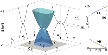
Increasing the electric field beyond the critical value () splits the Dirac point into two. The Dirac points () move away from the point along the X direction as a function of electric field [see Fig. 4(a)]. In the low-energy, two-band Hamiltonian (2), takes the form
| (7) |
where is the value of the inverted gap shown in Fig. 4(a). At each Dirac point, the Hamiltonian can be expanded in terms of , which gives us the low-energy form , a generic Dirac Hamiltonian with anisotropic Fermi velocity and ultimately the dispersion relation
| (8) |
Based on this dispersion, the Berry phase, , can be calculated by integrating the Berry potential, , over a closed path around each Dirac point; the integration path chosen here is a circle around each Dirac point, depicted in Fig. 4(a). is obtained from both the two-band low-energy and TB Hamiltonians. park2011berry ; resta2000manifestations This means that electrons in biased multilayer phosphorene carry an extra degree of freedom called the pseudospin. Dirac fermions exhibit unconventional quantum Hall effect, where LLs vary with as zhang2005experimental ; yuan2016quantum . The magnetic-field dependencies of the CB and VB edge of multilayer phosphorene biased at are shown in Figs. 4(b). As can be seen, both CB and VB (yellow circles) follow the square root power law of Dirac fermions (blue lines).
4 Metallic Phosphorene Nanoribbons in a Vertical Electric Field. Dual-Edge-Gate Device
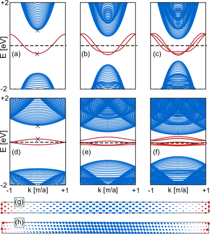
Nanoribbons are quasi-1D systems with a high length-to-width ratio, often fashioned from the ultrathin quasi-2D materials. The nanoribbon geometry is more amenable to device applications than the quasi-2D sheet geometry, and the electronic properties of ultranarrow nanoribbons are very sensitive to edge termination. Phosphorene nanoribbons, in particular, can combine the effects of band structure anisotropy and sensitivity to external fields, which characterize the underlying 2D phosphorene, with the effects of edges to give rise to unique electronic properties. Indeed, armchair and zigzag PNRs nanoribbons have been attracting a lot of attention in recent years carvalho2014phosphorene ; Guo2014JPCC ; peng2014edge ; Ramasubramaniam2014abinitio ; Ali2015JPhysD , with skewed-armchair nanoribbons having come into focus more recently grujic2016tunable . Here, we are specifically interested in metallic PNRs, which are found among skewed-armchair and zigzag PNRs [see Figs. 5(a) and 5(b), respectively]. These metallic PNRs have interesting behavior in a vertical electric field, which, as we will show, gives rise to new potential device functionalities. Other types of PNRs are insulating and will not be considered in this paper grujic2016tunable ; sisakht2015scaling ; carvalho2014phosphorene .
The calculated band structures of mono-, bi-, and trilayer zigzag PNRs are shown in Figs. 6(a)–(c) and those corresponding to skewed-armchair PNRs are shown in Figs. 6(d)–6(f), respectively. One can see the presence of midgap bands (red curves) completely detached from the bulk bands (shown in blue). For zigzag PNRs, each layer of phosphorene contributes one band of twofold-degenerate midgap states, making a total of two, four, six midgap states for mono-, bi- and trilayer PNRs, respectively. However, in the case of skewed-armchair PNRs, each layer provides two, twofold-degenerate midgap states. As a result, a total of four, eight, twelve midgap bands are present for mono-, bi- and trilayer skewed-armchair PNRs, respectively. We used the same tight-binding parameters for the PNRs as in the bulk calculation (Table 1). Of course, there is generally no guarantee that the bulk tight-binding parameters remain suitable for nanoribbons. However, there are at present no published DFT calculations for skewed PNRs against which we could benchmark tight-binding parameters. For ZPNRs, DFT calculations predict the existence of midgap bands carvalho2014phosphorene , as does tight binding. For ultranarrow ZPNRs (width below 3 nm), the dispersions of midgap bands found using DFT Guo2014JPCC differ somewhat from those predicted by the tight-binding model with bulk parameters sisakht2015scaling , but as the width of the ribbons increases and the gap between the bulk bands decreases, the results from the TB model become more consistent with the dispersions predicted by DFT Ramasubramaniam2014abinitio .
In the absence of a vertical electric field, zigzag PNRs are metallic since the Fermi level passes through all midgap bands and is far from the bulk states. In a similar manner, metallicity of skewed-armchair PNRs is caused by the two midgap states closest to the Fermi level without any contribution from the bulk states [see Figs. 6(d)-6(f)]. Therefore, near-equilibrium electronic transport in metallic PNRs is governed by midgap states. In Figs. 6(g) and 6(h), we plot the probability density for two wave functions marked in Figs. 6(a) and 6(d), respectively, one from a midgap band (shown in red) and another from the bulk CB (shown in blue). In contrast to the states from the bulk bands, whose probability density peaks near the PNR middle, the midgap state’s probability density is highest by the edges (near one edge in the top sublayer and near the other end in the bottom sublayer of a given monolayer). Therefore, electronic transport in PNRs should be tunable by the manipulation of the midgap states, confined to the edges.
Based on this finding, we propose a field-effect transistor (FET) shown in Fig. 7(a), where the conductance in PNRs via the midgap states (which are confined near the edges) is modulated locally by two edge gates, with voltages and . The width of the ribbons () is chosen to be nm, wide enough for experimental realization yet narrow enough to be computationally feasible via atomistic TB and nonequilibrium Green’s functions (NEGF) datta1997electronic . The width of each edge gate () is nm and the drain voltage () is fixed at mV. Figure 7(b) and (d) shows the band dispersion for zigzag and skewed armchair PNRs for V respectively. The applied bias strongly affects the midgap states, which have a high probability density right under the gate. The field induced by the bias shifts the bands whose wave function is localized in the upper sublayer upwards and shift the bands whose wave function is in the lower sublayer downward.
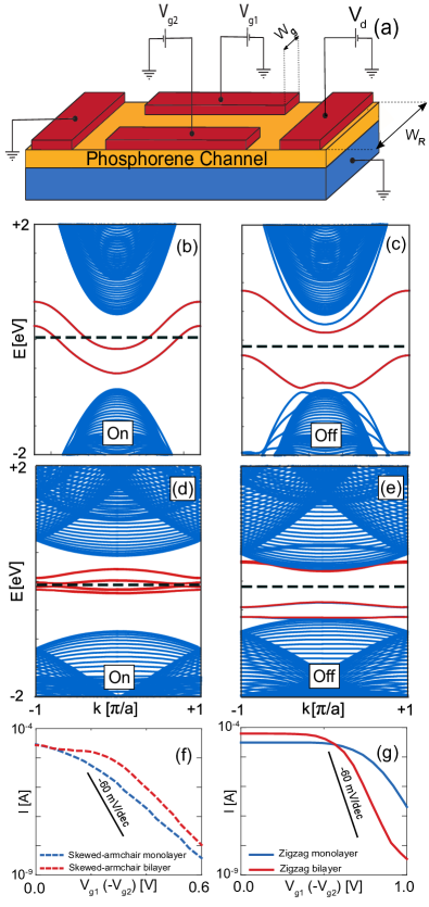
These edge gates have essentially no effect on the bulk bands. Although the midgap states have moved toward the bulk bands compared to their initial position in the gap [see Figs. 6(b) and 6(e)], the ribbon remains metallic since the Fermi level [which is fixed by the potentials on the source and drain on the left and right, Fig. 7(a)] still passes through the midgap bands. Increasing the bias voltages to V in Figs. 7(c) and 7(e) leads to a further energy separation of the midgap bands, so there are no states at the Fermi level, which denotes a transition from conducting [Fig. 6(b) and (d)] to insulating behavior [Fig. 6(c) and 6(e)].
This transition is also demonstrated by calculating the current for single and bilayer PNRs at room temperature ()) [Figs. 7(f) and (g) for skewed-armchair and zigzag PNRs] using the ballistic NEGF formalism. datta1997electronic . We implemented the low-field ballistic NEGF transport technique without self-consistent electrostatics in a fairly standard way: equilibrium Green’s functions are calculated at a given energy for the open system PNR system, where the role of contacts is incorporated in the NEGF via contact self-energies using the Sancho-Rubio iterative scheme SanchoRubio85 . The calculation of Green’s functions is performed for a dense array of energies within the transport window, i.e., over the energy range between the source and drain Fermi levels (50 meV) plus/minus several around this range ( is the Boltzmann constant). The edge gates are at potentials and with respect to the body potential, which is assumed zero, (i.e., body is grounded). The influence of the edge gates is incorporated into the relevant diagonal terms in the tight-binding Hamiltonian. It is assumed that the potential drops linearly over the PNR thickness, from the values of and at the top, underneath the gates, to zero at the bottom; in other words, the vertical field is constant under the gates. The points at the top of the PNR that are not under a gate are assigned zero potential. Finally, in the tight-binding NEGF transport calculation, the PNRs as implemented have lengths and widths in the several-nanometer range, but the actual lengths do not matter in the purely ballistic limit, as it is assumed that the edge gates go along the whole length of the PNR.
At low bias on the edge gates, the current [Fig. 7(f)] is relatively high, indicating that midgap states are crossing the Fermi level or located at the vicinity of Fermi level. As the voltage magnitude increases, the midgap states are pushed apart. Above a threshold bias on the edge gates, the current becomes vanishingly small, demonstrating a transition to an insulator [Fig. 7(f)]. This dual-edge-gate structure is compatible with current fabrication technology, as similar multigate structures were realized previously craciun2009trilayer ; williams2011gate . For single and bilayer zigzag PNRs [Fig. 7(g)], the subthreshold swing (SS) values are 115 and 80 mV/decade, respectively. In case of single layer and bilayer skewed-armchair PNRs [Fig. 7(f)], the SS values are 136 and 112 mV/decade, respectively. For reference, we also added the 60 mV/decade SS curves to Fig. 7(f) and (g), which would correspond with the turn-off theoretical limit in Si MOSFETs. The values obtained are lower than the 5 V/decade obtained for bulk-phosphorene field-effect transistors Li2014NatureNano , they are still higher than the SS in commercial silicon-based devices (70 mV/decade).
A recent calculation showed that edge functionalization can lead to a dramatic flattening of the midgap-band dispersions peng2014edge , which would significantly reduce the threshold voltage required for the conductor-to-insulator transition. As the current in the on-state is channeled by the midgap states, the SS will be dependent on the dispersion of midgap states. Edge passivation of PNRs leads to almost dispersion-free midgap states peng2014edge , and this effect could approximately be captured in the tight-binding model by setting ezawa2014topological . Indeed, our preliminary calculations with yield a SS of 15 mV/decade, which is below the theoretical limit for ideal MOSFETs Choi2007IEEE_EDL . This result hints that edge-passivated PNRs might be promising as field-effect switches.
5 Conclusion
In summary, we showed that the electron band dispersion for multilayer phosphorene transitions from parabolic in the zigzag and massive Dirac fermion in the armchair direction at vertical electric fields below to a dispersion of an anisotropic massless Dirac fermion at electric fields above . We posited that this transition would be observed in quantum Hall experiments as an electric-field-dependent change in the Landau-level energy vs : below , at , and above .
Moreover, we showed that selective tuning of midgap bands in metallic PNRs results in novel device functionalities. We proposed a structure with dual edge gates that strongly affect the edge states associated with the midgap bands, but leave the bulk ones inert. The dual-edge-gate structure can induce a transition from a conducting “on” state to an insulating “off” state by moving the midgap bands away from the Fermi level, thereby realizing field-effect transistor action on PNRs.
Electric-field modulation of phosphorene and PNRs is a versatile concept that can enable access to new physics and new functions in phosphorene-based devices.
6 Acknowledgement
The work was primarily supported by the NSF (DMR-1121288) through the University of Wisconsin Materials Research Science and Engineering Center (MRSEC) seed project. After the end of the NSF seed support, funding by the University of Wisconsin – Madison through the Patricia and Michael Splinter Professorship in Electrical and Computer Engineering (awarded to I.K.) enabled successful completion of this work. The work was performed using the resources of the UW-Madison Center for High Throughput Computing (CHTC).
References
- (1) W. Lu, et al. Plasma-assisted fabrication of monolayer phosphorene and its raman characterization. Nano Research, 7, 6, 853 (2014).
- (2) H. Liu, et al. Phosphorene: an unexplored 2d semiconductor with a high hole mobility. ACS Nano, 8, 4, 4033 (2014).
- (3) S. Zhang, et al. Extraordinary photoluminescence and strong temperature/angle-dependent raman responses in few-layer phosphorene. ACS Nano, 8, 9, 9590 (2014).
- (4) V. Tran, et al. Layer-controlled band gap and anisotropic excitons in few-layer black phosphorus. Phys.Rev.B, 89, 23, 235319 (2014).
- (5) Y. Jing, et al. Small molecules make big differences: molecular doping effects on electronic and optical properties of phosphorene. Nanotechnology, 26, 9, 095201 (2015).
- (6) M. Buscema, et al. Fast and broadband photoresponse of few-layer black phosphorus field-effect transistors. Nano.Lett, 14, 6, 3347 (2014).
- (7) S. P. Koenig, et al. Electric field effect in ultrathin black phosphorus. App.Phys.Lett, 104, 10, 103106 (2014).
- (8) F. Xia, H. Wang, and Y. Jia. Rediscovering black phosphorus as an anisotropic layered material for optoelectronics and electronics. Nature Communications, 5 (2014).
- (9) D. Çakır, C. Sevik, and F. M. Peeters. Significant effect of stacking on the electronic and optical properties of few-layer black phosphorus. Phys.Rev.B, 92, 16, 165406 (2015).
- (10) D. Çakır, H. Sahin, and F. M. Peeters. Tuning of the electronic and optical properties of single-layer black phosphorus by strain. Phys.Rev.B, 90, 20, 205421 (2014).
- (11) R. Fei and L. Yang. Strain-engineering the anisotropic electrical conductance of few-layer black phosphorus. Nano.Lett, 14, 5, 2884 (2014).
- (12) R. Fei, et al. Enhanced thermoelectric efficiency via orthogonal electrical and thermal conductances in phosphorene. Nano.Lett, 14, 11, 6393 (2014).
- (13) S. Yuan, A. Rudenko, and M. Katsnelson. Transport and optical properties of single-and bilayer black phosphorus with defects. Phys.Rev.B, 91, 11, 115436 (2015).
- (14) G. Qin, et al. Anisotropic intrinsic lattice thermal conductivity of phosphorene from first principles. Physical Chemistry Chemical Physics, 17, 7, 4854 (2015).
- (15) Y. Cai, et al. Giant phononic anisotropy and unusual anharmonicity of phosphorene: Interlayer coupling and strain engineering. Advanced Functional Materials, 25, 15, 2230 (2015).
- (16) T. Low, et al. Plasmons and screening in monolayer and multilayer black phosphorus. Phys.Rev.Lett, 113, 10, 106802 (2014).
- (17) M. Elahi, et al. Modulation of electronic and mechanical properties of phosphorene through strain. Phys.Rev.B, 91, 11, 115412 (2015).
- (18) S. Das, et al. Tunable transport gap in phosphorene. Nano.Lett, 14, 10, 5733 (2014).
- (19) J. Kim, et al. Observation of tunable band gap and anisotropic dirac semimetal state in black phosphorus. Science, 349, 6249, 723 (2015).
- (20) C. Dutreix, E. Stepanov, and M. Katsnelson. Laser-induced topological transitions in phosphorene with inversion symmetry. Phys.Rev.B, 93, 24, 241404 (2016).
- (21) Q. Liu, et al. Switching a normal insulator into a topological insulator via electric field with application to phosphorene. Nano.Lett, 15, 2, 1222 (2015).
- (22) T. Low, Y. Jiang, and F. Guinea. Topological currents in black phosphorus with broken inversion symmetry. Phys.Rev.B, 92, 23, 235447 (2015).
- (23) A. Carvalho, A. Rodin, and A. C. Neto. Phosphorene nanoribbons. EPL (Europhysics Letters), 108, 4, 47005 (2014).
- (24) H. Guo, et al. Phosphorene nanoribbons, phosphorus nanotubes, and van der waals multilayers. The Journal of Physical Chemistry C, 118, 25, 14051 (2014).
- (25) M. Ali, M. Keshtan, and M. Esmaeilzadeh. Spin filtering in a magnetized zigzag phosphorene nanoribbon. Journal of Physics D: Applied Physics, 48, 48, 485301 (2015).
- (26) X. Peng, A. Copple, and Q. Wei. Edge effects on the electronic properties of phosphorene nanoribbons. Journal of Applied Physics, 116, 14, 144301 (2014).
- (27) A. Rudenko, S. Yuan, and M. Katsnelson. Toward a realistic description of multilayer black phosphorus: From g w approximation to large-scale tight-binding simulations. Phys.Rev.B, 92, 8, 085419 (2015).
- (28) A. N. Rudenko and M. I. Katsnelson. Quasiparticle band structure and tight-binding model for single-and bilayer black phosphorus. Phys.Rev.B, 89, 20, 201408 (2014).
- (29) S. Weinberg. Gravitation and cosmology: principles and applications of the general theory of relativity, volume 1. Wiley New York (1972).
- (30) X. Zhou, et al. Landau levels and magneto-transport property of monolayer phosphorene. Scientific Reports, 5 (2015).
- (31) J. Pereira Jr and M. Katsnelson. Landau levels of single-layer and bilayer phosphorene. Phys.Rev.B, 92, 7, 075437 (2015).
- (32) A. Ghazaryan and T. Chakraborty. Aspects of anisotropic fractional quantum hall effect in phosphorene. Phys.Rev.B, 92, 16, 165409 (2015).
- (33) P. G. Harper. Single band motion of conduction electrons in a uniform magnetic field. Proceedings of the Physical Society. Section A, 68, 10, 874 (1955).
- (34) D. Thouless, et al. Quantized hall conductance in a two-dimensional periodic potential. Phys.Rev.Lett, 49, 6, 405 (1982).
- (35) K. Wakabayashi, et al. Electronic and magnetic properties of nanographite ribbons. Phys.Rev.B, 59, 12, 8271 (1999).
- (36) P. Wiegmann and A. Zabrodin. Bethe-ansatz for the bloch electron in magnetic field. Phys.Rev.Lett, 72, 12, 1890 (1994).
- (37) Z. Jiang, et al. Infrared spectroscopy of landau levels of graphene. Phys. Rev. Lett., 98, 197403 (2007).
- (38) S. Yuan, et al. Quantum hall effect and semiconductor-to-semimetal transition in biased black phosphorus. Phys.Rev.B, 93, 24, 245433 (2016).
- (39) Y. Hasegawa, et al. Zero modes of tight-binding electrons on the honeycomb lattice. Phys.Rev.B, 74, 3, 033413 (2006).
- (40) The condition for energy levels in a magnetic field is , where is the area of constant-energy surface in reciprocal space lifshitz1956theory . Since , the Landau levels are found to be for multilayer phosphorene at the critical electric field.
- (41) P. Dietl, F. Piéchon, and G. Montambaux. New magnetic field dependence of landau levels in a graphenelike structure. Phys.Rev.Lett, 100, 23, 236405 (2008).
- (42) G. Montambaux, et al. Merging of dirac points in a two-dimensional crystal. Phys.Rev.B, 80, 15, 153412 (2009).
- (43) G. Montambaux, et al. A universal hamiltonian for motion and merging of dirac points in a two-dimensional crystal. The European Physical Journal B, 72, 4, 509 (2009).
- (44) C.-H. Park and N. Marzari. Berry phase and pseudospin winding number in bilayer graphene. Phys.Rev.B, 84, 20, 205440 (2011).
- (45) R. Resta. Manifestations of berry’s phase in molecules and condensed matter. Journal of Physics: Condensed Matter, 12, 9, R107 (2000).
- (46) Y. Zhang, et al. Experimental observation of the quantum hall effect and berry’s phase in graphene. Nature, 438, 7065, 201 (2005).
- (47) A. Ramasubramaniam and A. R. Muniz. Ab initio studies of thermodynamic and electronic properties of phosphorene nanoribbons. Phys. Rev. B, 90, 085424 (2014).
- (48) M. M. Grujić, et al. Tunable skewed edges in puckered structures. Phys.Rev.B, 93, 24, 245413 (2016).
- (49) E. T. Sisakht, M. H. Zare, and F. Fazileh. Scaling laws of band gaps of phosphorene nanoribbons: a tight-binding calculation. Phys.Rev.B, 91, 8, 085409 (2015).
- (50) S. Datta. Electronic transport in mesoscopic systems. Cambridge university press (1997).
- (51) M. P. L. Sancho, et al. Highly convergent schemes for the calculation of bulk and surface green functions. Journal of Physics F: Metal Physics, 15, 4, 851 (1985).
- (52) M. Craciun, et al. Trilayer graphene is a semimetal with a gate-tunable band overlap. Nature Nano, 4, 6, 383 (2009).
- (53) J. Williams, et al. Gate-controlled guiding of electrons in graphene. Nature Nano, 6, 4, 222 (2011).
- (54) L. Li, et al. Black phosphorus field-effect transistors. Nature Nano., 9, 372 (2014).
- (55) M. Ezawa. Topological origin of quasi-flat edge band in phosphorene. New Journal of Physics, 16, 11, 115004 (2014).
- (56) W. Y. Choi, et al. Tunneling field-effect transistors (tfets) with subthreshold swing (ss) less than 60 mv/dec. IEEE Electron Device Letters, 28, 8, 743 (2007). ISSN 0741-3106.
- (57) I. Lifshitz and A. Kosevich. Theory of magnetic susceptibility in metals at low temperatures. Sov. Phys. JETP, 2, 636 (1956).