Tunable spin-orbit coupling and symmetry-protected edge states in graphene/WS2
Abstract
We demonstrate clear weak anti-localization (WAL) effect arising from induced Rashba spin-orbit coupling (SOC) in WS2-covered single-layer and bilayer graphene devices. Contrary to the uncovered region of a shared single-layer graphene flake, WAL in WS2-covered graphene occurs over a wide range of carrier densities on both electron and hole sides. At high carrier densities, we estimate the Rashba SOC relaxation rate to be and show that it can be tuned by transverse electric fields. In addition to the Rashba SOC, we also predict the existence of a‘valley-Zeeman’ SOC from first-principles calculations. The interplay between these two SOC’s can open a non-topological but interesting gap in graphene; in particular, zigzag boundaries host four sub-gap edge states protected by time-reversal and crystalline symmetries. The graphene/WS2 system provides a possible platform for these novel edge states.
Introduction. Electron pseudospin in graphene and the associated chirality yield remarkable transport consequences including the half-integer quantum Hall effect Yuanbo Zhang and Kim (2005) and intrinsic weak anti-localization (WAL) Ando et al. (1998). Physical spin, by contrast, is often largely a spectator that couples weakly to momentum due to carbon’s low mass, leading to much longer spin diffusion lengths ( at room temperature) than normal conductors Tombros et al. (2007); Han and Kawakami (2011). Graphene’s extremely weak spin-orbit coupling (SOC) clearly has merits, yet greatly hinders the observation of important spin-dependent phenomena including the quantum spin Hall effect Kane and Mele (2005) and quantum anomalous Hall effect Qiao et al. (2010). Fortunately, the open two-dimensional honeycomb structure allows tailoring the SOC strength by coupling to foreign atoms or materials Castro Neto and Guinea (2009); Weeks et al. (2011); Ding et al. (2011); Hu et al. (2012); Ma et al. (2012); Jin and Jhi (2013); Ferreira et al. (2014). Several experiments have pursued approaches of graphene hydrogenation Kaverzin and van Wees (2015); Balakrishnan et al. (2013) or fluorination Hong et al. (2011) as well as heavy-adatom decoration Jia et al. (2015); Chandni et al. (2015); these methods tend to decrease the transport quality, and moreover the induced SOC appears either difficult to reproduce Kaverzin and van Wees (2015); Balakrishnan et al. (2013) or to detect Hong et al. (2011); Jia et al. (2015); Chandni et al. (2015). A different approach has recently been employed by several groups: placing graphene on target substrates featuring heavy atoms. Proximity to the substrates not only provides desirable properties such as ferromagnetic ordering and large SOC, but also reduces adverse effects on the target materials Wang et al. (2015a); Jiang et al. (2015); Avs (2014); Wang et al. (2015b).
Here we employ magneto-conductance (MC) measurements to demonstrate enhanced SOC in graphene proximity-coupled to multilayer WS2. We quantify the spin-relaxation rate caused by Rashba SOC by fitting to WAL data, and further show that the Rashba strength is tunable via transverse electric fields. Guided by first-principles calculations, we also predict that WS2-covered graphene additionally features a prominent ‘valley-Zeeman’ SOC that mimics a Zeeman field with opposite signs for the two valleys. The interplay between these two SOC terms opens a non-topological gap at the Dirac point that supports symmetry-protected sub-gap edge states along certain boundaries. Though the gap is too small to be detected in our experiments, theory suggests that graphene/WS2 may provide a simple model system for studying such an unusual gapped phase.
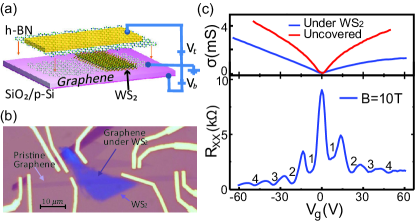
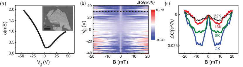
Experimental Setup. Figure 1(a) sketches the dual-gated graphene devices used in our study. Both single-layer graphene and multilayer WS2 flakes were first exfoliated from their respective bulk materials and subsequently placed onto a Si/SiO2 () wafer. Since multilayer WS2 flakes can be much thicker and are less likely deformed, we chose to transfer the WS2 flake instead of graphene to avoid trapped bubbles in between, thereby yielding a larger effective overlap area. Figure 1(b) shows an optical image of the device prior to top-gate fabrication. Notice that only part of the graphene channel directly contacts with WS2; the left uncovered channel serves as a control sample that allows direct comparison with the right part under WS2 (dark blue).
Transport measurements were performed at 2K (unless specified otherwise) using a Quantum Design’s Physical Property Measurement System. Figure 1(c), top, shows the conductivity of graphene versus the back gate voltage. Interestingly, for both top and back gate sweeps, the device does not show the conductivity saturation (up to with back gate) reported recently by other groups Avs (2014); Wang et al. (2015b). Conductivity saturation in the latter studies was attributed to saturation in carrier density from either the large density of states associated with sulfide defects Avs (2014) or screening by electrons in the WS2/SiO2 interface Wang et al. (2015b). In our WS2-covered device, the lack of conductivity saturation on either side suggests that the Fermi level resides within the band gap of WS2, consistent with our DFT calculations (see below). The absence of the carrier density saturation in graphene is verified by Shubnikov-de Haas oscillations of the WS2-covered graphene as a function of the gate voltage in a magnetic field; see Figure 1(c). On both sides, the Landau Levels are evenly spaced up to the 4th level, indicating that the carrier density is proportional to the gate voltage. This property allows us to access the high-density regions, which is important for understanding the origin of enhanced SOC and accurately determining its strength. The field effect mobility, calculated from capacitance of the SiO2 Chen et al. (2008) layer, is higher in the uncovered graphene () than the WS2-covered graphene ( on the hole side, and on the electron side). Despite the relatively low mobility, our devices manifest clear low-field magneto-conductance (MC) over a much larger carrier-density range than in previous studies Wang et al. (2015b); Avs (2014).
Rashba SOC Signature. Due to its unusual chirality, graphene with smooth disorder is predicted to exhibit WAL Ando et al. (1998). However, strong inter-valley scattering, which typically arises in ordinary-quality samples, suppresses the chirality-related WAL and generates weak localization (WL) McCann et al. (2006); Tikhonenko et al. (2008). Introducing strong Rashba SOC allows the spin relaxation rate to exceed the inelastic dephasing rate . In this case, before quantum dephasing occurs the electron spin precesses around the effective magnetic field and acquires an additional phase in the interference McCann and Fal’ko (2012)—reviving WAL due to spin. Intrinsic (Kane-Mele) and valley-Zeeman SOC terms, by contrast, break an effective time reversal symmetry and thus place the system in the unitary class (suppressed WL) McCann and Fal’ko (2012).
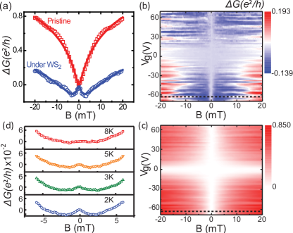
Figure 2(a) contrasts the low-temperature MC for uncovered and WS2-covered devices at approximately the same carrier density, [corresponding to the black dashed lines in Figs. 2(b) and (c)]. The uncovered graphene shows WL as expected given the modest mobility. More interestingly, in WS2-covered graphene the MC clearly exhibits the hallmark WAL feature at low fields. In both cases this behavior persists over a broad range of gate voltages as shown in Figs. 2(b) and (c). The robust WAL feature appearing only in the WS2-covered graphene—despite its lower mobility which naively further promotes WL—provides strong evidence of Rashba SOC acquired from WS2 on both electron and hole sides. This result differs qualitatively from the strongly asymmetric characteristic reported in Ref. Avs, 2014; there the induced SOC was only observed on the electron side, which was attributed to the asymmetric density-of-states due to sulfur vacancies.
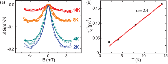
To further confirm the proximity-induced SOC, we fabricated a WS2-covered bilayer-graphene device. Unlike in single-layer graphene, WL is expected independent of inter-valley scattering strength in bilayer graphene due to its associated Berry phase Gorbachev et al. (2007). Consequently, the emergence of WAL in a bilayer graphene—which we indeed detect—gives direct evidence of Rashba SOC inherited from WS2 (i.e., the competing pseudospin interpretation disappears here). Figure 2(d) shows the observed WAL feature in a bilayer-graphene device at different temperatures. Note that we only measure a clear WAL signature when the carrier density exceeds , suggesting that the dominant dephasing mechanism in bilayer graphene is electron-electron interaction. In this scenario, increasing the carrier density suppresses dephasing, and WAL appears once the dephasing rate drops below the spin relaxation rate. The WAL feature also disappears on raising temperature, due naturally to thermally enhanced dephasing.
It is worth mentioning that the MC data shown in Figure 2 are from single field-sweep measurements, as opposed to an ensemble average Tikhonenko et al. (2009); Wang et al. (2015b) over many curves taken over a gate-voltage range corresponding to the Thouless energy. Our device length () greatly exceeds the coherence length (); hence the conductivity self-averages resulting in suppressed universal conductance fluctuations (UCF) Datta (1995).
Quantitative Analysis. When inter- and intra-valley scattering rates are much larger than the dephasing and spin relaxation rates, MC in graphene is well-described at low magnetic fields by the following expression from diagrammatic perturbation theory McCann and Fal’ko (2012):
| (1) | |||||
Here ( is the digamma function) and with the diffusion constant. The spin relaxation rate is determined by the asymmetric Rashba SOC , i.e., , while follows from those symmetric SOCs including the intrinsic SOC , and valley-Zeeman SOC . (Additional SOC terms that may be present due to the system’s low symmetry are assumed negligible for simplicity.)
The intrinsic SOC relaxation rate obeys the Elliot-Yafet mechanism Elliott (1954); Yafet (1963); Ochoa et al. (2012): , where is the momentum relaxation rate and is the Fermi energy. This rate is thus negligibly small compared to the typical dephasing rate in graphene when . Here we deliberately focus on the high-carrier-density region ( and ) where we can reasonably approximate . The coupling meanwhile is inherited from WS2 due to sublattice symmetry breaking Xiao et al. (2012). Since this term imposes an opposite Zeeman field for the two valleys, it generates non-degenerate, spin-polarized momentum eigenstates whose spin orientations do not relax (except due to the interplay with other SOCs). Thus the valley-Zeeman SOC relaxation rate is also negligible. With these assumptions only and remain in Eq. (1), and both can be extracted by fitting to the experimental data [see, e.g., blue curve in Fig. 2(a)].
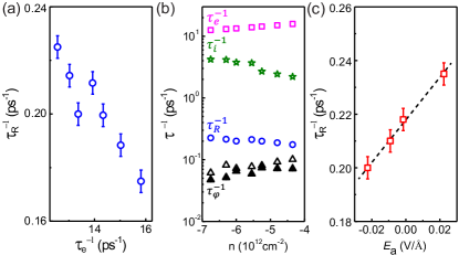
Figure 3(a) shows the resulting for WS2-covered graphene as a function of the momentum scattering rate calculated from the device mobility Rengel and Martín (2013). As increases, the Rashba SOC relaxation rate decreases almost monotonically, indicating that the spin relaxation is dominated by the Dyakonov-Perel mechanism 15. Dyakonov and Perel (1972) []. This behavior stands in marked contrast to standalone graphene, in which the Elliot-Yafet mechanism dominates spin relaxation over a broad range of carrier density Han and Kawakami (2011); Kaverzin and van Wees (2015). Furthermore, the spin relaxation rate of WS2-covered graphene () exceeds that for standalone graphene (e.g., Han and Kawakami (2011)) by two orders of magnitude—indicating strong SOC introduced by the proximity coupling with WS2.
Figure 3(b) displays the density dependence of the characteristic relaxation rates. All data correspond to WS2-covered graphene except the inter-valley scattering rate . The latter is extracted by fitting our WL data for uncovered graphene with the theory of Ref. McCann et al., 2006 instead of Eq. (1); as an example, see the red curve in Fig. 2(a). [Equation (1) can also provide a good fit for our low-field WL measurements in the absence of any SOC terms, but does not reveal .] We assume that inferred from uncovered graphene sets a lower bound for the corresponding rate in WS2-covered graphene,which is quite natural given its lower mobility. From Fig. 3(b) we then see that —a prerequisite for Eq. (1)—is indeed satisfied for WS2/graphene. Moreover, the dephasing rate can be extracted independently from the WAL, or the UCF by the autocorrelation function Lee et al. (1987) (see Supplementary Material for details), and both methods agree quite well. These facts support the applicability of Eq. (1) and suggest that the spin relaxation rates we extracted from the high-carrier density region are reliable.
Our dual-gated graphene device [Fig. 1(a)] allows us to study the influence of an applied transverse electric field on the Rashba SOC. In particular, the dual gate enables independent control of the carrier density (thus the momentum scattering rate) and the transverse electric field Sui et al. (2015). Figure 3(c) shows the spin relaxation rate extracted at fixed but at different transverse electric fields (for the field points from WS2 to graphene). Interestingly, increases monotonically with the applied field, changing by 18% over the range -60V/300nm to 60V/300nm. This increase can be interpreted as an enhancement of the Rashba SOC: The positive electric field lifts the graphene Dirac bands towards the WS2 conduction bands Yu et al. (2009); hence graphene’s orbitals acquire a stronger hybridization with the tungsten orbitals, substantially strengthening Rashba SOC.
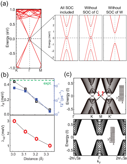
Origin and implications of SOC. To explain these experimental findings we performed density-functional theory (DFT) calculations using a large supercell in the lateral plane ( graphene on WS2) that minimizes the lattice mismatch () between these two materials. With the van der Waals correction, the optimized interlayer distance is , and a small buckling () is found in the graphene layer. The Dirac cones in Fig. 4(a) still center around the Fermi level, indicating negligible charge transfer between WS2 and graphene as seen experimentally [in all our devices the graphene is slightly p-doped (), as generally observed for substrates]. The zoom-in of the band structure reveals a sizable spin splitting and a gap at the Dirac point due to SOC and the loss of sublattice symmetry. To diagnose the origin of the SOC terms, we adjust the SOC strength of each element selectively; see rightmost panels of Fig. 4(a). When SOC of carbon is excluded, the band structure remains essentially unchanged. However, eliminating the SOC for tungsten removes the spin splitting and yields a trivial mass gap, unrelated to SOC, that simply reflects the staggered sublattice potential induced by WS2. Enhanced SOC of graphene is thus primarily induced by hybridization with tungsten atoms.
We analytically model our DFT results with the low-energy Hamiltonian
| (2) | |||||
The first line represents the standard Dirac theory supplemented by a staggered sublattice potential , while the second encodes symmetry-allowed SOC terms 111Note that inter-valley terms are excluded here even though the system is a superlattice; the supplementary material provides evidence that they are unimportant in this case.. DFT bands near the Dirac point for the optimized structure can be well-fit using Eq. (2) with the following parameters: , , and .
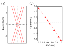
The fitted SOC strengths do, however, depend sensitively on the interlayer distance in the DFT simulations. Figure 4(b) presents the interlayer-distance dependence of the two dominant SOCs, and . The Rashba spin relaxation rates shown are calculated through , with a value ps-1 comparable to that extracted from experiment. We find that DFT for the optimized structure underestimates the Rashba coupling seen experimentally, but that this difference can be mitigated by using smaller interlayer distances. This ‘correction’ is not unreasonable given imperfections in our samples and the neglect of the weak force between graphene and WS2 in DFT calculations. The reduced distance also increases in DFT; its effect, however, is likely artificially enhanced by the use of a parallelogram supercell that breaks sublattice symmetry, which is arguably restored in an average sense by the incommensuration of real samples. On the contrary, we expect that incommensuration more weakly impacts , which only requires asymmetry.
Together, these two SOCs open a gap at the neutrality point— lifts spin degeneracy while gaps the remaining carriers via spin-flip processes. This gapped state is not a topological insulator (contrary to the reports of previous DFT studies Gmitra et al. (2016); Wang et al. (2015b)), as can be verified by the existence of an even number of counter-propagating edge states and explicit calculations of the topological invariant in a lattice model. Figure 4(c) shows the tight-binding band structure for a strip with zigzag (top) and armchair (bottom) edges, including both and SOCs. In the zigzag case two copies of edge states appear at , points due to band inversion, as observed in Ref. Gmitra et al., 2016, but two more edge states also appear at the -point. These edge states are protected by time reversal and crystalline symmetries, but do not have a topological origin. For an armchair geometry, no edge states appear.
This gapped phase, while topologically trivial, exhibits edge-state properties that differ markedly from those of the valley Hall effect driven by an ordinary mass gap Xiao et al. (2007); Sui et al. (2015). Both exhibit edge states along zigzag boundaries, but with very different spin polarizations. For the SOC gap, the -point edge states exhibit out-of-plane spin polarization while those at and exhibit in-plane polarization. In contrast, valley-Hall-effect edge modes are spin degenerate and thus do not naturally support spin currents. The nontrivial spin structure for the edge modes in our problem, combined with the prospect of electrically tuning Rashba coupling and hence the band gap, underlie tantalizing applications for spintronics that warrant further pursuit.
Conclusion. We have demonstrated a dramatic and tunable enhancement of Rashba SOC in graphene by coupling to WS2. In the high carrier-density region, we determined the Rashba coupling strength by analyzing the low-field MC. First-principles calculations indicate that the induced SOC originates from the band hybridization between graphene orbitals and tungsten states. The combination of Rashba and a theoretically predicted valley-Zeeman SOC creates novel edge states that are interesting to pursue further by engineering heterostructures with different substrates as well as improving the device mobilities.
Acknowledgments. We gratefully acknowledge Roger Mong for valuable discussions. This work was supported by the DOE BES award No. DE-FG02-07ER46351 (BY and JS) and award No. DE-FG02-05ER46237 (JW and RW); NSF through grant DMR-1341822 (MT and JA); the Caltech Institute for Quantum Information and Matter, an NSF Physics Frontiers Center with support of the Gordon and Betty Moore Foundation; and the Walter Burke Institute for Theoretical Physics at Caltech. DFT simulations were performed on the U.S. Department of Energy Supercomputer Facility (NERSC).
References
- Yuanbo Zhang and Kim (2005) H. L. S. Yuanbo Zhang, Yan-Wen Tan and P. Kim, Nature 438, 201 (2005).
- Ando et al. (1998) T. Ando, T. Nakanishi, and R. Saito, Journal of the Physical Society of Japan 67, 2857 (1998), http://dx.doi.org/10.1143/JPSJ.67.2857 .
- Tombros et al. (2007) N. Tombros, M. P. Csaba Jozsa, H. T. Jonkman, and B. J. van Wees, Nature 448, 571 (2007).
- Han and Kawakami (2011) W. Han and R. K. Kawakami, Phys. Rev. Lett. 107, 047207 (2011).
- Kane and Mele (2005) C. L. Kane and E. J. Mele, Phys. Rev. Lett. 95, 226801 (2005).
- Qiao et al. (2010) Z. Qiao, S. A. Yang, W. Feng, W.-K. Tse, J. Ding, Y. Yao, J. Wang, and Q. Niu, Phys. Rev. B 82, 161414 (2010).
- Castro Neto and Guinea (2009) A. H. Castro Neto and F. Guinea, Phys. Rev. Lett. 103, 026804 (2009).
- Weeks et al. (2011) C. Weeks, J. Hu, J. Alicea, M. Franz, and R. Wu, Phys. Rev. X 1, 021001 (2011).
- Ding et al. (2011) J. Ding, Z. Qiao, W. Feng, Y. Yao, and Q. Niu, Phys. Rev. B 84, 195444 (2011).
- Hu et al. (2012) J. Hu, J. Alicea, R. Wu, and M. Franz, Phys. Rev. Lett. 109, 266801 (2012).
- Ma et al. (2012) D. Ma, Z. Li, and Z. Yang, Carbon 50, 297 (2012).
- Jin and Jhi (2013) K.-H. Jin and S.-H. Jhi, Phys. Rev. B 87, 075442 (2013).
- Ferreira et al. (2014) A. Ferreira, T. G. Rappoport, M. A. Cazalilla, and A. H. Castro Neto, Phys. Rev. Lett. 112, 066601 (2014).
- Kaverzin and van Wees (2015) A. A. Kaverzin and B. J. van Wees, Phys. Rev. B 91, 165412 (2015).
- Balakrishnan et al. (2013) J. Balakrishnan, G. K. W. Koon, M. Jaiswal, A. H. C. Neto, and B. C. Ozyilmaz, Nat. Phys. 9, 284 (2013).
- Hong et al. (2011) X. Hong, S.-H. Cheng, C. Herding, and J. Zhu, Phys. Rev. B 83, 085410 (2011).
- Jia et al. (2015) Z. Jia, B. Yan, J. Niu, Q. Han, R. Zhu, D. Yu, and X. Wu, Phys. Rev. B 91, 085411 (2015).
- Chandni et al. (2015) U. Chandni, E. A. Henriksen, and J. P. Eisenstein, Phys. Rev. B 91, 245402 (2015).
- Wang et al. (2015a) Z. Wang, C. Tang, R. Sachs, Y. Barlas, and J. Shi, Phys. Rev. Lett. 114, 016603 (2015a).
- Jiang et al. (2015) Z. Jiang, C.-Z. Chang, C. Tang, P. Wei, J. S. Moodera, and J. Shi, Nano Letters 15, 5835 (2015), pMID: 26288309, http://dx.doi.org/10.1021/acs.nanolett.5b01905 .
- Avs (2014) Nat Commun 5, 4875 (2014).
- Wang et al. (2015b) Z. Wang, D.-K. Ki, H. Chen, H. Berger, A. H. MacDonald, and A. F. Morpurgo, Nat Commun 6, 8339 (2015b).
- Chen et al. (2008) J.-H. Chen, C. Jang, S. Adam, M. S. Fuhrer, E. D. Williams, and M. Ishigami, Nat Phys 4, 377 (2008).
- McCann et al. (2006) E. McCann, K. Kechedzhi, V. I. Fal’ko, H. Suzuura, T. Ando, and B. L. Altshuler, Phys. Rev. Lett. 97, 146805 (2006).
- Tikhonenko et al. (2008) F. V. Tikhonenko, D. W. Horsell, R. V. Gorbachev, and A. K. Savchenko, Phys. Rev. Lett. 100, 056802 (2008).
- McCann and Fal’ko (2012) E. McCann and V. I. Fal’ko, Phys. Rev. Lett. 108, 166606 (2012).
- Gorbachev et al. (2007) R. V. Gorbachev, F. V. Tikhonenko, A. S. Mayorov, D. W. Horsell, and A. K. Savchenko, Phys. Rev. Lett. 98, 176805 (2007).
- Tikhonenko et al. (2009) F. V. Tikhonenko, A. A. Kozikov, A. K. Savchenko, and R. V. Gorbachev, Phys. Rev. Lett. 103, 226801 (2009).
- Datta (1995) S. Datta, Electronic Transport in Mesoscopic Systems, 3rd ed. (Cambridge University Press, 1995).
- Elliott (1954) R. J. Elliott, Phys. Rev. 96, 266 (1954).
- Yafet (1963) Y. Yafet, Solid State Physics (Academic, New York, 1963).
- Ochoa et al. (2012) H. Ochoa, A. H. Castro Neto, and F. Guinea, Phys. Rev. Lett. 108, 206808 (2012).
- Xiao et al. (2012) D. Xiao, G.-B. Liu, W. Feng, X. Xu, and W. Yao, Phys. Rev. Lett. 108, 196802 (2012).
- Rengel and Martín (2013) R. Rengel and M. J. Martín, Journal of Applied Physics 114, 143702 (2013), http://dx.doi.org/10.1063/1.4824182.
- 15. Dyakonov and Perel (1972) M. 15. Dyakonov and V. Perel, Sov. Phys. Solid State 13, 3023 (1972).
- Lee et al. (1987) P. A. Lee, A. D. Stone, and H. Fukuyama, Phys. Rev. B 35, 1039 (1987).
- Sui et al. (2015) M. Sui, G. Chen, W.-Y. S. Liguo Ma, D. Tian, K. Watanabe, T. Taniguchi, X. Jin, W. Yao, D. Xiao, and Y. Zhang, Nat Phys 11, 1027 (2015).
- Yu et al. (2009) Y.-J. Yu, Y. Zhao, S. Ryu, L. E. Brus, K. S. Kim, and P. Kim, Nano Letters 9, 3430 (2009), pMID: 19719145, http://dx.doi.org/10.1021/nl901572a .
- Note (1) Note that inter-valley terms are excluded here even though the system is a superlattice; the supplementary material provides evidence that they are unimportant in this case.
- Gmitra et al. (2016) M. Gmitra, D. Kochan, P. Högl, and J. Fabian, Phys. Rev. B 93, 155104 (2016).
- Xiao et al. (2007) D. Xiao, W. Yao, and Q. Niu, Phys. Rev. Lett. 99, 236809 (2007).
- Altshuler et al. (1982) B. L. Altshuler, A. G. Aronov, and D. E. Khmelnitsky, Journal of Physics C: Solid State Physics 15, 7367 (1982).
- Narozhny et al. (2002) B. N. Narozhny, G. Zala, and I. L. Aleiner, Phys. Rev. B 65, 180202 (2002).
- Kresse and Joubert (1999) G. Kresse and D. Joubert, Phys. Rev. B 59, 1758 (1999).
- Blöchl (1994) P. E. Blöchl, Phys. Rev. B 50, 17953 (1994).
- Perdew et al. (1996) J. P. Perdew, K. Burke, and M. Ernzerhof, Phys. Rev. Lett. 77, 3865 (1996).
- Grimme et al. (2010) S. Grimme, J. Antony, S. Ehrlich, and H. Krieg, The Journal of Chemical Physics 132, 154104 (2010), http://dx.doi.org/10.1063/1.3382344.
I Supplementary Information
II Method and experimental setup
The target WS2 flake was identified with an optical microscope and then transferred to cover part of the long graphene channel. To promote adhesion, the wafer was annealed in O2 at for 3 hours. Standard electron-beam lithography and electron-beam evaporation were used to connect the graphene with multiple thick Au electrodes. The electrodes allow independent four-terminal resistivity measurements in the covered and uncovered areas. After fabrication of electrodes, an h-BN flake was transferred to cover the whole device to serve as a top gate dielectric, followed by the top Au gate metal fabrication with similar electron-beam lithography procedures. No additional annealing was performed thereafter.
III Reproducible WAL in a single-layer graphene on WS2 device
Here we present a second device that has the similar characteristics as the first one shown in the main text. Instead of transferring WS2 onto graphene, in this second sample we transferred graphene onto WS2, in order to show that the absence of density saturation is independent of the transfer sequence and robustness of WAL exists. Figure S 1(a) shows the conductivity of graphene versus gate voltage. This device exhibits almost the same properties as the device in the main text, despite its lower mobility ( on the hole side, and on the electron side), which is mainly due to the bubbles in the device. As clearly seen in the inset, bubbles (small black dots) appear across the graphene flake. We intentionally did not choose a bubble-free area in order to minimize the UCFs. Figure S 1(b) shows the WAL features observed in this device at different gate voltages. Compared to the first sample, MC is smallerhere. We symmetrize the data to show clearer temperature dependence, as is shown in Figure S 1(c). Just as in the first device, WAL is present on both hole and electron sides and disappears quickly as temperature increases.
IV Temperature dependence of MC
Figure S 2(a) shows the temperature dependence of the MC data of the WS2-covered graphene. Compared with the spin diffusion length and the SOC scattering rate Han and Kawakami (2011), the inelastic dephasing rate is much more sensitive to temperature at low temperatures; thus the dramatic decrease of the WAL signal can be primarily attributed to the significantly increased inelastic dephasing rate. The extracted dephasing rate as a function of temperature appears in Fig. S 2(b). We find that obeys approximately a linear temperature dependence, which can be explained by the electron-electron scattering in the diffusive regime Altshuler et al. (1982),
| (S 1) |
where is a correction coefficient equal to . If the graphene mobility is extremely high, the sample will reach the ballistic regime () and the temperature dependence of will turn parabolic Narozhny et al. (2002). Under this circumstance, Eq. (1) will also be rendered invalid since it is developed for the diffusive regime. However, since our device has a moderate mobility of , it is well in the diffusive transport regime (); therefore Eq. (1) is applicable. At low temperatures, the dephasing time appears to start deviating from the straight line. In principle, at low temperatures the electron-electron scattering may not be the dominant inelastic scattering mechanism, as compared with electron-phonon interactions, the spin-flip scattering of electrons from localized spins McCann and Fal’ko (2012), etc.
V Universal conduction fluctuations (UCF)
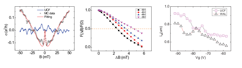
Universal conductance fluctuations can be extracted by removing the WAL background in the MC, as shown in Fig. S 3(a). The WAL curve is fitted by Eq. 1 and describes the experimental data quite well up to 50 mT. In addition to the reproducibility of the MC curves, the nearly symmetric fluctuations in conductance as a function of magnetic field provides further evidence that for UCF.
To calculate the phase coherence length from the UCF, we utilized the autocorrelation function to find the characteristic magnetic field , which is determined by . Figure S 3(b) shows the normalized autocorrelation function at different gate voltages. When the device approaches a higher carrier density, the characteristic field clearly decreases, indicating an increase in the phase coherence length due to the weaker electron-electron interaction than the Dirac region. The s extracted from UCF agree reasonably well with those extracted from WAL, as shown in Fig. S 3(c), suggesting the validity of Eq. (1) and thus the extracted spin-orbit scattering rates.
VI DFT Computational details
Our first-principles calculations were carried out using the projected augmented plane-wave method Kresse and Joubert (1999); Blöchl (1994) as implemented in the Vienna ab initio simulation package. The valence electron configuration for C, W, and S is , , and , respectively. Generalized gradient approximation of Perdew-Burke-Ernzerhof type was used for the description of exchange-correlation interactions among electrons Perdew et al. (1996). Spin-orbit coupling was included in the self-consistent calculation level. We employed -point grid for Graphene/WS2 heterostructure containing C, W and S atoms. A large supercell was adopted to minimize the lattice mismatch; most of our simulations correspond to a supercell with graphene on WS2 (see, however, the next section). Slab structures were separated by Å of vacuum along the surface normal. The energy cutoff for the plane-wave-basis expansion was set to . Positions of all atoms were fully relaxed until the convergence of total energies became better than . In order to treat the van der Waals force properly, we adopted the DFT-D3 method suggested by Ref. Grimme et al., 2010.
VII Effect of the supercell size on the low-energy states
With a graphene unit cell, the Dirac cones are folded to point. Consequently, spurious interaction between the valleys may appear in our DFT calculations. To verify that the induced SOC of graphene is not sensitive to the chosen cell size, we repeated the simulations for a different supercell. Specifically, we adopted graphene in contact with a WS2 monolayer so that the and valleys reside at distinct momenta. The lattice mismatch increases to whereas the separation between graphene and WS2 decreases to Å. Although we used a different supercell, band energies near the Dirac point remain essentially the same as shown in Fig. S 4(a). We also found that the Dirac cones are very sensitive to the SOC strength. Figure S 4(b) shows that the band order becomes inverted at the and points as SOC is turned on from zero to its physical value (we checked that the same band inversion occurs in the graphene supercell). We can therefore conclude that the enhancement of SOC is only weakly affected by the specific atomic configuration and that inter-valley coupling provides a rather minor effect even when the Dirac cones are shifted to the same momentum.
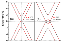
VIII Fitting the model Hamiltonian to first-principles calculations
By matching energies from the model Hamiltonian in Eq. (2) with DFT calculations, we determined the following parameters for a () graphene supercell: , , and for the () supercell. From Fig. S 5 we see that high-quality fits are possible for either interlayer separation.