Topological Dirac semimetal phases in InSb/-Sn semiconductor superlattices
Abstract
We demonstrate theoretically the coexistence of Dirac semimetal and topological insulator phases in InSb/-Sn conventional semiconductor superlattices, based on advanced first-principles calculations combined with low-energy theory. By proper interfaces designing, a large interface polarization emerges when the growth direction is chosen along [111]. Such an intrinsic polarized electrostatic field reduces band gap largely and invert the band structure finally, leading to emerge of the topological Dirac semimetal phase with a pair of Dirac nodes appearing along the (111) crystallographic direction near the point. The surface states and Fermi arc are clearly observed in (100) projected surface. In addition, we also find a two-dimensional topological insulator phase with large nontrivial band gap approaching 70 meV, which make it possible to observe the quantum spin Hall effect at room temperature. Our proposal paves a way to realize topological nontrivial phases coexisted in conventional semiconductor superlattices by proper interface designing.
pacs:
73.21.La, 73.22.Dj, 73.22.Gk, 73.20.At,Band topology of solids has attracted intensive and broad interest in the past decade due to the discovery of two-dimensional (2D) and three-dimensional (3D) topological insulators. Topological insulators posses a bulk gap and gapless boundary states protected by the topology of bulk energy bands. These materials have been intensively investigated both theoretically and experimentally in recent years because of symmetry-protected dissipationless transport property PhysRevLett.95.226801 ; RevModPhys.82.3045 ; RevModPhys.83.1057 ; S. Murakami ; A. Roth . The massless fermions emerge in topological insulator edges/surfacesRevModPhys.83.1057 ; PhysRevLett.98.106803 , and topological Dirac and Weyl semimetalsPhysRevLett.108.140405 ; PhysRevB.83.205101 ; PhysRevLett.107.127205 ; PhysRevX.5.011029 . Among the distinct topological nontrivial phases, Dirac semimetals are of particular interests, because the Dirac semimetals can be selectively driven into other topological nontrivial phases such as topological insulators and Weyl semimetals by specific symmetry breaking e.g., inversion symmetry or time-reversal symmetry. Up to date, various principles have been proposed to search and classify Dirac semimetals protected by certain symmetryncomms5898 ; PhysRevLett.115.126803 , and limited candidates such as Bi(=Na,K,Rb), have been foundPhysRevB.85.195320 ; PhysRevB.88.125427 . For deepening understanding of transitions between distinct topological nontrivial phases and broadening the application horizon of the topological phases, it is highly desirable to construct topological insulators, Weyl and Dirac semimetals by artificial designing in conventional semiconductors. The early attempts to design topological insulator phase in semiconductors were firstly proposed in the GaN/InN/GaNPhysRevLett.109.186803 and later in GaAs/Ge/GaAsPhysRevLett.111.156402 quantum wells (QWs) utilizing interface engineering. Recently, a few experimental groups observe such huge interface electric fieldnphys1814 ; PhysRevB.88.125310 and the signature of topological phase1.4902916 . Recent theoretical works also prove this interface polarization induced topological insulator phases in other systemsPhysRevLett.112.216803 ; nl5043769 ; adfm.201505357 .
In this work, we demonstrate theoretically that the Dirac semimetal phase can emerge in InSb/-Sn semiconductor superlattices (SLs). -Sn is a well-known semimetalGapless-Semiconductors ; PhysRevB.87.235307 because the s-like band is lower than the p-like band due to the relativistic mass-Darwin effect. -Sn can be tuned to be topological insulators by applying external strainPhysRevLett.111.216401 ; PhysRevLett.111.157205 . However, ARPES and spin-resolved transport measurements reveal that the Dirac-cones of the systems are buried below the Fermi surface about 100 meVPhysRevLett.111.157205 . The zinc-blende InSb is a semiconductor with a direct narrow bandgap located at point, and the lattice mismatch between InSb (6.480Å) and -Sn (6.489Å) is about 0.14%. Such a small lattice mismatch can effectively decrease defects, vacancies, and dislocations on the interfaces, and make InSb a perfect partner to resemble heterostructures with -Sn. Molecular beam epitaxy experiments reveal that InSb/-Sn/InSb [111] heterostructures can be fabricated with sharp interfaces and the interface polarization can be maintained thereinPhysRevLett.72.2596 , which makes our proposal achievable experimentally accessible.
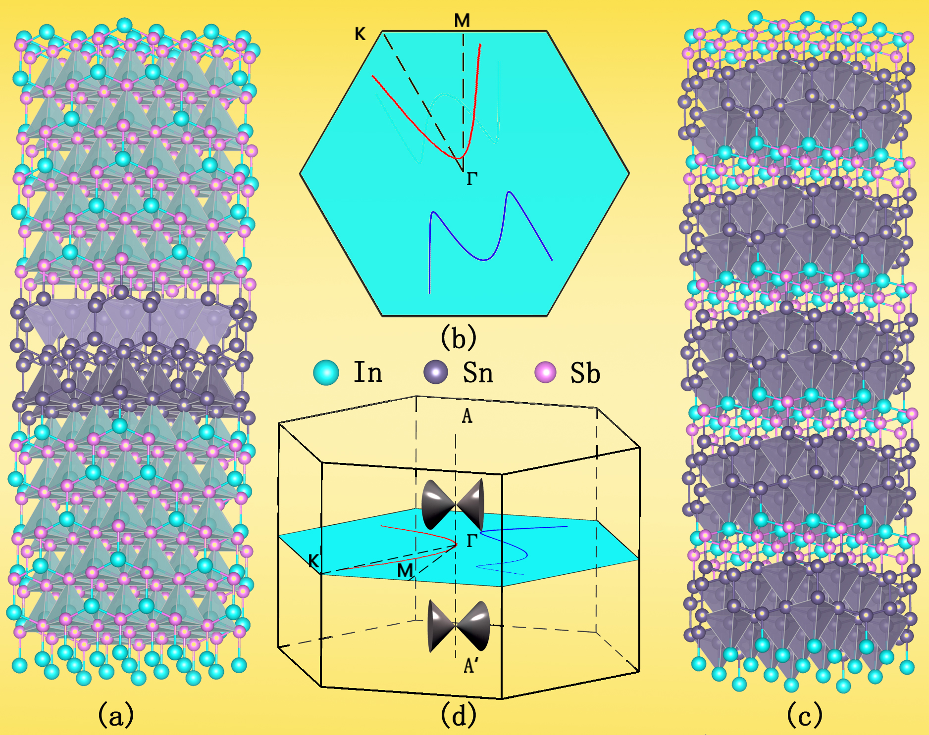
Fig. 1 shows the superlattices consisted of atomically-thin InSb and -Sn layers stacked periodically along the [111] direction of the zinc-blende bulk materials. There is a huge intrinsic polarized electric field arising from opposite charge accumulations at adjacent interfaces. This electric field can reduce the bandgap significantly and generate a strong Rashba spin-orbital coupling (SOC) effect. This field also depends sensitively on the thicknesses of -Sn and InSb layers. For the thick InSb layer, the polarized electric field decreases rapidly and the electron wave functions in each -Sn layers are decoupled and are isolated completely, in analogy to a single QW case, as illustrated as in Fig. 1(a) and (b). As the thickness of the InSb layers decreases, the overlapping of adjacent -Sn layers is no longer negligible and the energy dispersions along direction cannot be neglected, see Fig. 1(d).
In order to investigate the band structures of InSb/-Sn superlattices, we adopted the advanced first-principle calculationPhysRev.136.B864 performed by the Vienna ab initio Simulation Package (VASP)PhysRevB.54.11169 with the local density approximation (LDA)PhysRev.140.A1133 . The electron-ion interaction is described by pseudopotentials that are generated within the projector-augmented wave (PAW) methodPhysRevB.59.1758 . A plane wave basis set with a kinetic energy cutoff of 560 eV for bulk calculations and the superlattices is used. For bulk Brillouin-zone integrations, a mesh of 111111 -centered k points are usedPhysRevB.13.5188 . For the thick SLs case, we use the -centered Monkhorst-Pack scheme to sample the Brillouin zone, and the mesh of k-point sampling is 773. The convergence criterion of the self-consistency process is set to be eV. Since the accuracy of the band gap is particular importance in our study, we applied Tran-Blaha method with the modified Becke-Johnson (MBJ) semilocal exchange functional, named MBJLDA methodPhysRevLett.102.226401 to correct the underestimations of bandgap from traditional DFT-LDA. The method has been proved successful and effective in many zinc-blende compoundsPhysRevB.82.205212 ; PhysRevB.80.035203 and in our cases (see Supplementary Part ISupplement ), we find the equally setting parameter CMBJ=1.200 for InSb and -Sn could produce reliable band gaps for bulk materials and heterostures. Moreover, to capture topological phase transitions in the heterostructures, the SOC effects are taken into accounts in all the calculations.
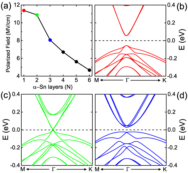
First, we calculate the electronic structures of InSb/-Sn SLs with thick InSb layers, to ensure isolation between electrons in adjacent layers, modeled by supercells consisting of 12 atomic bilayers. In order to understand the evolution of the electronic structures, we shows the energy spectra for different -Sn bilayers (N=1,2,3) in Figs. 2 (b)-(d), respectively. Considering the different atom bondings at the upper and lower interfaces in the InSb/-Sn superlattice structures shown in Fig. 1(a), Sn-Sb bonds at the upper interface and Sn-In bonds at the lower interface, negative and positive charges accumulate at upper and lower interfaces due to the charge transfer between Sn and Sb (In) atoms, respectively and create an intrinsic polarized electric field crossing the -Sn layers. From Fig. 2(a), one can find out that the polarized field can be as large as 11.2 MV/cm when there is only one bilayer Sn sandwiched in two adjacent thick InSb layers and decreases rapidly to 4.8 MV/cm for six Sn bilayers due to the charge transfer in the adjacent interfaces. At the same time, the increasing of the thickness of -Sn weakens the quantum confinement effect dramatically, as a consequence, from Fig. 2(b), one can see that the quantum confinement effect is so strong that the QW system possesses a normal band order and a trivial band gap about 100 meV even under such a huge electric field (11.2 MV/cm). When the thickness of the Sn layers increases to 3 bilayers, as illustrated in Fig. 2(d), the polarized electric field play a dominant role, the conduction and valence bands are inverted with a nontrivial band gap as large as 70 meV, which means the quantum spin Hall effect in such systems can be observed at room temperature. This nontrivial gap is much larger than the nontrivial gaps in HgTe QWs (about 10meV) and InAs/GaSb QWs (about 5meV). This topological insulator phase transition occurs because of i) the decrease of band gap caused by the interface polarized electric field; and ii) the strong intrinsic SOC in -Sn ( eV) layers and InSb ( eV) layers. Fig. 2(c) indicates the critical thickness of -Sn layer for the topological insulator phase transition. In the electronic structures of a single -Sn bilayer sandwiched by thick InSb layers. A single four-fold degenerated Dirac point emerges locating rightly at the Fermi energy, which can be viewed as a a 3D Dirac semimetal with anisotropic energy dispersion as an analogue to its 3D counterpart observed in HgCdTe semiconductor nphys2857 . This 2D Kane fermion system bridges the topological insulator phase and trivial insulator phase. The 2D Kane Fermion can maintain a 3D Dirac semimetal with anisotropic energy dispersion, e.g., quantum well case (see the on-line supplemental material, Part IISupplement ).
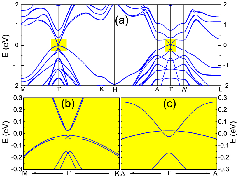
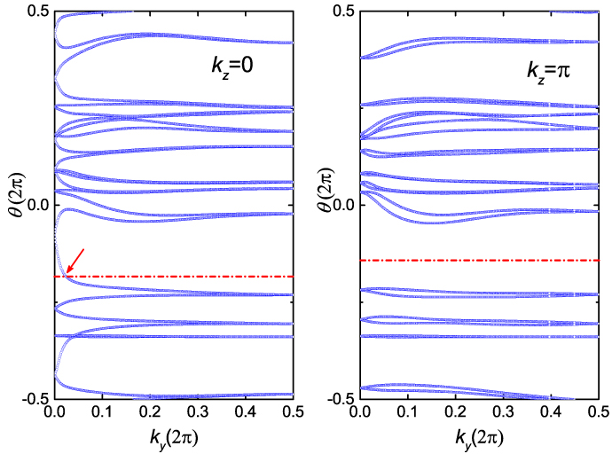
Next, we turn to search a topological Dirac semimetal phase in InSb/-Sn superlattices. We calculate the band structures of a series of short-period InSb/-Sn superlattices. Considering the shortest superlattice consisting of 3 atomic bilayers, in which two bilayers of -Sn are sandwiched by one bilayer InSb to take full advantage of polarized field and the quantum confinement effect, the first-principles calculation including the SOC reveals the SL is a semimetal. Fig. 3(a) shows the band structures is gapless in the vicinity of the Fermi energy in the full Brillouin zone. The highlighted regions in Fig. 3(a) are amplified in Figs. 3 (b) and (c), respectively. Fig. 3(b) clearly depicts a nontrivial band gap opening, i.e., the TI phase, just the same as in Fig. 2(d), but with a smaller gap. More importantly, in Fig 3(c), a pair of Dirac points emerge at time-reversal points along the axis in vicinity of point. The two touching points possessing linear dispersions and keeping unaffected in presence of SOC in companion with nontrivial index indicate Dirac semimetal phase in the superlattice. The topological indices of the InSb/-Sn superlattices are calculated by study of the evolution of the Wannier charge centers (WCCs) in =0 and = two-dimensional subsystems explicitlyWCC1 ; WCC2 , see Fig.4. The superlattice is topologically nontrivial since the number of transitions of WCC remains odd with respect to arbitrary reference lines.
Furthermore, the calculation of the Fermi surface and surface states are performed to confirm the Dirac semimetal phase. We consider that a InSb/-Sn SL can be cleaved along a certain crystallographic plane, forming a semi-infinite slab, a tight-binding Hamiltonian was obtained with maximally localized Wannier function (MLWF)PhysRevB.56.12847 ; PhysRevB.65.035109 derivated from the first-principles calculations. The surface Green’s function of the semi-infinite slab was constructed from the tight-binding Hamiltonian via iterative methods016 ; 009 , whose imaginary part corresponds to the local density of states (LDOS) at the surface.
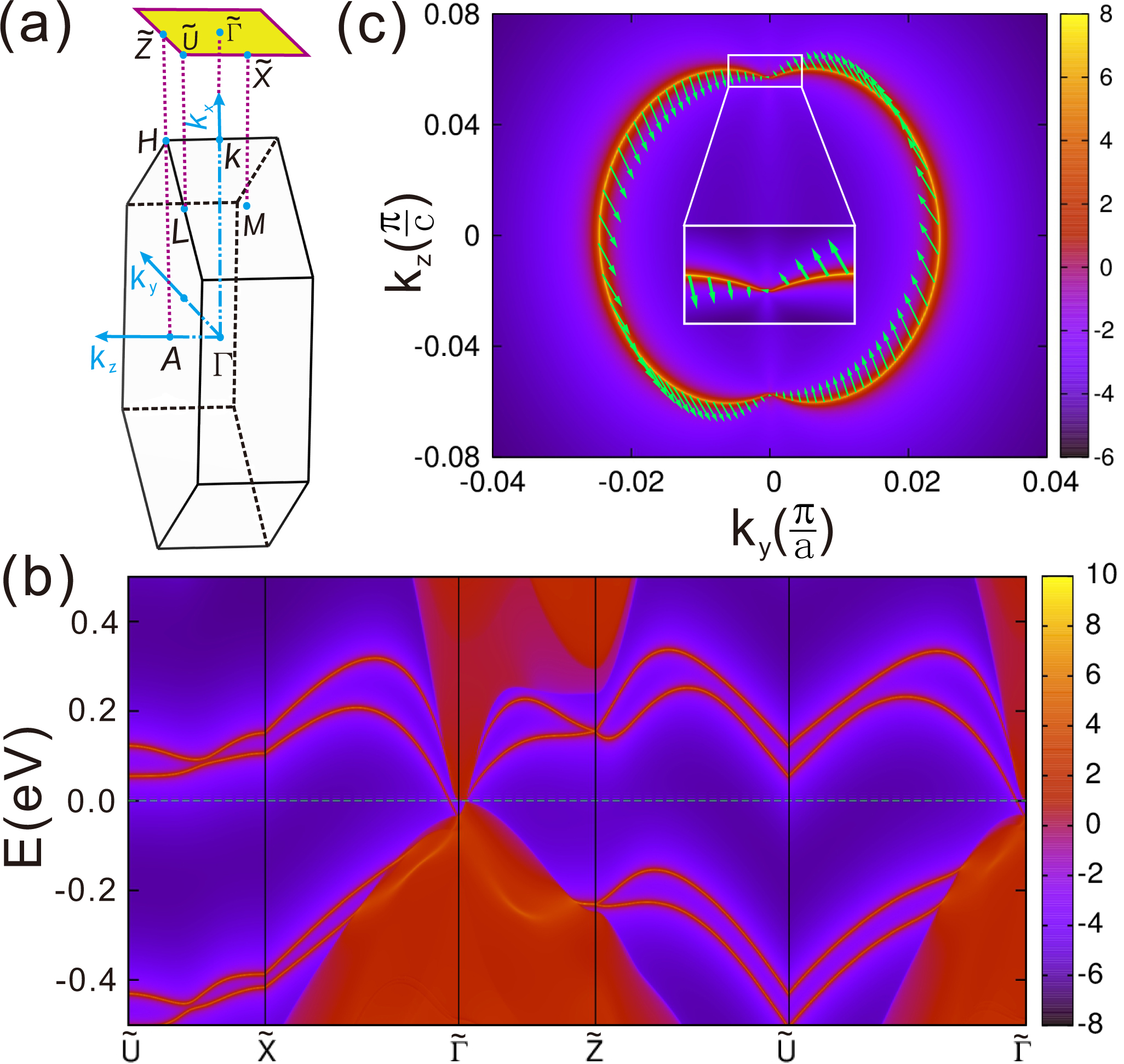
If the InSb/-Sn superlattices are cleaved along (100) crystallographic surface, the energy dispersions of the bulk and surface states in the full Brillouin zone (see Fig. 5(b)) are projected to a 2D Brillouin zone (see Fig. 5 (a)). One can clearly see a Fermi loop in Fig. 5(c), which is composed of two half-circle Fermi arcs connected by two singular points which are corresponding to Dirac points in bulk band structure of the superlattice. The spin texture is superposed on the Fermi loop by analysis of the local spin density and suggests the chirality of the Fermi loop. In addition, the dissipationless surface states are shown in Fig. 5(b). The dissipationless surface states in companion with the Fermi loop are typical fingerprints of 3D topological Dirac semimetals.
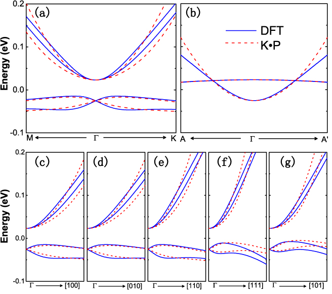
To capture the essential physics of the Dirac semimetal phase, we deviated a low-energy effective Hamiltonian. Since the first-principles calculation unveil that, the low energy states mainly origin from and orbital with two different angular momentum , we chose the four bases set of . By utilizing the theory of invariantsPhysRevB.82.045122 , the effective Hamiltonian around point reads
where . The Hamiltonian take very similar form as the model Hamiltonian for topological insulators with new off-diagonal elements. The terms containing the high order contribution is required by the threefold rotational symmetry, and the off-diagonal elements describes the SOC caused by the broken inversion symmetry. Actually, one can get an effective Hamiltonian for describing InSb/-Sn/InSb QWs by simply set =0. And on the other hand, set ==0 and diagonalize the effective Hamiltonian, one can get two Dirac points located at . For the specific superlattice in this work, we obtained the parameters in the effective Hamiltonian by fitting energy spectrum of effective model with that obtained from first-principles calculations, , where take minus signs to demonstrate the band inversion. From Fig. 6 , one can find out that, the energy dispersions calculated from the effective Hamiltonian are in good agreement with the first-principles calculations in vicinity of the point. Each fourfold degenerated Dirac point is created by band inversion, and can be classified as topological Dirac semimetals created by band inversion in previous workncomms5898 . The topological Dirac semimetal phase can be widely maintained in InSb/-Sn superlattices (see Supplementary Part III).
In summary, we studied systematically the electronic structures of InSb/-Sn superlattices. The first-principles calculations reveal the coexistence of topological insulator phase and 3D topological Dirac semimetal phases with a large nontrivial gap (70 meV) in the conventional semiconductor InSb/-Sn superlattice by utilizing polarized interfaces therein, and the topological phases could be tuned by well-developed semiconductor growth techniques. Our proposal paves a way to design topological nontrivial phases in semiconductor materials and provides a unified platform to observe topological phase transitions at room temperature.
This work was supported by Grant No. 2015CB921503 from the MOST of China and NSFC Grants No. 11504366, and No. 11434010.
References
- (1) C. L. Kane and E. J. Mele, Phys. Rev. Lett. 95, 226801 (2005).
- (2) M. Z. Hasan and C. L. Kane, Rev. Mod. Phys. 82, 3045 (2010).
- (3) X. L. Qi and S. C. Zhang, Rev. Mod. Phys. 83, 1057 (2011).
- (4) S. Murakami, N. Nagaosa, and S. C. Zhang, Science 301, 1348 (2003).
- (5) A. Roth, C. Brüne, H. Buhmann, L.W. Molenkamp, J. Maciejko, X.-L. Qi, and S.-C. Zhang, Science 325, 294 (2009).
- (6) L. Fu, C. L. Kane, and E. J. Mele, Phys. Rev. Lett 98, 106803 (2007).
- (7) S. M. Young, S. Zaheer, J. C. Y. Teo, C. L. Kane, E. J. Mele, and A. M. Rappe, Phys. Rev. Lett. 108, 140405 (2012).
- (8) X. Wan, A. M. Turner, A. Vishwanath, and S. Y. Savrasov, Phys. Rev. B 83, 205101 (2011).
- (9) A. A. Burkov and L. Balents, Phys. Rev. Lett. 107, 127205 (2011).
- (10) H. Weng, C. Fang, Z. Fang, B. A. Bernevig, and X. Dai, Phys. Rev. X 5, 011029 (2015).
- (11) B. J. Yang and N. Nagaosa, Nature Communications 5, 4898 (2014).
- (12) S. M. Young and C. L. Kane, Phys. Rev. Lett. 115, 126803 (2015).
- (13) Z. Wang, Y. Sun, X.-Q. Chen, C. Franchini, G. Xu, H. Weng, X. Dai, and Z. Fang, Phys. Rev. B 85, 195320 (2012).
- (14) Z. Wang, H. Weng, Q. Wu, X. Dai, and Z. Fang, Phys. Rev. B 88, 125427 (2013).
- (15) M. S. Miao, Q. Yan, C. G. Van de Walle, W. K. Lou, L. L. Li, and K. Chang, Phys. Rev. Lett. 109, 186803 (2012).
- (16) D. Zhang, W. Lou, M. Miao, S.-C. Zhang, and K. Chang, Phys. Rev. Lett. 111, 156402 (2013).
- (17) G. Singh-Bhalla, C. Bell, J. Ravichandran, W. Siemons, Y. Hikita, S. Salahuddin, A. F. Hebard, H. Y. Hwang, and R. Ramesh, Nat. Phys. 7, 80 (2011).
- (18) L. Zhou, E. Dimakis, R. Hathwar, T. Aoki, D. J. Smith, T. D. Moustakas, S. M. Goodnick, and M. R. McCartney, Phys. Rev. B 88, 125310 (2013).
- (19) W. Pan, E. Dimakis, G. T. Wang, T. D. Moustakas, and D. C. Tsui, Appl. Phys. Lett. 105, 213503 (2014).
- (20) H. Zhang, Y. Xu, J. Wang, K. Chang, and S.-C. Zhang, Phys. Rev. Lett. 112, 216803 (2014).
- (21) Q. Liu, X. Zhang, L. B. Abdalla, A. Fazzio, and A. Zunger, Nano Lett. 15, 1222 (2015).
- (22) Q. Liu, X. Zhang, L. B. Abdalla, A. Zunger, Adv. Funct. Mater. 26, 3259 (2016).
- (23) I. Tsidilkowski, Gapless Semiconductors—A New Class of Materials (Akademie, Berlin, 1988).
- (24) S. K̈ufner, J. Furthmüller, L. Matthes, M. Fitzner, and F. Bechstedt, Phys. Rev. B 87, 235307 (2013).
- (25) Y. Ohtsubo, P. Le Fèvre, F. Bertran, and A. Taleb-Ibrahimi, Phys. Rev. Lett. 111, 216401 (2013).
- (26) A. Barfuss, L. Dudy, M. R. Scholz, H. Roth, P. Höpfner, C. Blumenstein, G. Landolt, J. H. Dil, N. C. Plumb, M. Radovic, A. Bostwick, E. Rotenberg, A. Fleszar, G. Bihlmayer, D. Wortmann, G. Li, W. Hanke, R. Claessen, and J. Schäfer, Phys. Rev. Lett. 111, 157205 (2013).
- (27) 31 H. Omi, H. Saito, and T. Osaka, Phys. Rev. Lett. 72, 2596 (1994).
- (28) P. Hohenberg and W. Kohn, Phys. Rev. B 136, 864 (1964).
- (29) G. Kresse and J. Furthmüller, Phys. Rev. B 54, 11169 (1996).
- (30) W. Kohn and L. J. Sham, Phys. Rev. 140, A1133 (1965).
- (31) G. Kresse and D. Joubert, Phys. Rev. B 59, 1758 (1999).
- (32) H. J. Monkhorst and J. D. Pack, Phys. Rev. B 13, 5188 (1976).
- (33) F. Tran and P. Blaha, Phys. Rev. Lett 102, 226401 (2009).
- (34) Y.-S. Kim, M. Marsman, G. Kresse, F. Tran, and P. Blaha, Phys. Rev. B 82, 205212 (2010).
- (35) Y.-S. Kim, K. Hummer, and G. Kresse, Phys. Rev. B 80, 035203 (2009).
- (36) See Supplemental Material at,
- (37) M. Orlita, D. M. Basko, M. S. Zholudev, F. Teppe, W. Knap, V. I. Gavrilenko, N. N. Mikhailov, S. A. Dvoretskii, P. Neugebauer, and C. Faugeras, Nat. Phys. 10, 233 (2014).
- (38) S. Küfner, L. Matthes and F. Bechstedt, Phys. Rev. B 93, 045304 (2016)
- (39) M. Taherinejad, K. F. Garrity, and D. Vanderbilt, Phys. Rev. B 89, 115102 (2014)
- (40) N. Marzari and D. Vanderbilt, Phys. Rev. B 56, 12847 (1997).
- (41) I. Souza, N. Marzari, and D. Vanderbilt, Phys. Rev. B 65, 035109 (2001).
- (42) M. P. L. Sancho, J. M. L. Sancho, and J. Rubio, Journal of Physics F: Metal Physics 14, 1205 (1984).
- (43) M. P. L. Sancho, J. M. L. Sancho, J. M. L. Sancho, and J. Rubio, Journal of Physics F: Metal Physics 15, 851 (1985).
- (44) C. X. Liu, X. L. Qi, H. J. Zhang, X. Dai, Z. Fang, and S. C. Zhang, Phys. Rev. B 82, 045122 (2010).