A versatile rotary-stage high frequency probe station for studying magnetic films and devices
Abstract
We present a rotary-stage microwave probe station suitable for magnetic films and spintronic devices. Two stages, one for field rotation from parallel to perpendicular to the sample plane (Out-of-Plane) and the other intended for field rotation within the sample plane (In-Plane) have been designed. The sample, probes and micro positioners are rotated simultaneously with the stages, which allows the field orientation to cover from 0 to and from 0 to . and being the angle between the direction of current flow and field in a Out-of-Plane and an In-Plane rotation, respectively. The operation frequency is up to 40 GHz and the magnetic field up to 1 T. The sample holder, vision system and probe assembly are compactly designed for the probes to land on a wafer with diameter up to 3 cm. Using homemade multi-pin probes and commercially available high frequency probes, several applications including 4-probe DC measurements, the determination of domain wall velocity and spin transfer torque ferromagnetic resonance are demonstrated.
I introduction
The discovery of spin transfer torque has attracted considerable attention in the past decade.(Slonczewski, 1996; Mangin et al., 2006; Rippard et al., 2004; Houssameddine et al., 2007; Ikeda et al., 2010) Recently, manipulation of magnetic bits through spin Hall effect(Liu et al., 2012) and spin orbit torque(Yu et al., 2014) have also been demonstrated. The characteristic time for current induced magnetic switching is ns and the typical frequency of spin torque driving response is in the GHz range. These findings have made magnetic nanodevices realistic candidates for memory and microwave device applications. In response, there has been increasing demand for microwave frequency probe stations capable of characterizing magnetic films and devices.
Various probe stations with variable temperature and magnetic field are commercially available. (Lake Shore Cryotronics, Inc. and Janis Research Company for example.) However, for room temperature applications, it is imperative to have the option of changing field direction with respect to the sample. This is especially important because magnetic materials are generally anisotropic and the effect of spin torque is angle dependent. Unfortunately, only a few solutions for the field rotation probe station are available. Technically, one needs to either rotate the magnet system or the sample. The former is favorable when signal stability is a major concern. Homemade vector magnets and projected field electromagnets (GMW associates) can provide a rotating magnetic field, however, the field uniformity is poor and the field strength is usually limited to a few kOe.(GMW, ) As detailed in a recent design,(Li et al., 2012) extra care must be taken to calibrate the magnets. Besides, close loop PID control is much more complicated for applications require precise field values. A magnet with rotating base, on the other hand, only enables the field rotation along a single axis. In the latter case, the commercial products have adopted sample stage rotation design to allow 360∘ of sample rotation within the film plane.(Lak, ; Jan, ) The orientation of the probes and the corresponding positioners are fixed. For devices working at low frequency (1 GHz), the DC probes can always be landed on the pads without any issue. However, in a high frequency (10 GHz) measurement, impedance match is of primary importance. Consequently, special probes with integrated tips such as ground-signal-ground (GSG) probes and coplanar waveguide type device pads should be used.(Mellnik et al., 2014) The misalignment between the probe and the pads of the device is usually limited to 30∘ for reliable measurement.(Wang et al., 2014) Several devices with identical pattern but different orientations must be measured to obtain device parameters as a function of field direction in the range of 0 to 360∘. In reality, geometry as well as magnetic property variations among sub-100 nm devices are inevitable. Furthermore, re-landing of the probes to the device is necessary for each sample orientation, which greatly increases the testing time, causes reliability issue and hinders fully automation.
Here, we present a compact and systematic solution for building a RF probe station with relative field orientation capable of rotating from parallel to perpendicular to the sample plane (out-of-plane (OP) rotation) as well as 360∘ rotation within the sample plane (in-plane (IP) rotation). The design is based on the idea of rotating sample, probes and microwave cables simultaneously, making the angular dependent measurement convenient and efficient. The test platform is suitable for studying magnetic films and devices from DC to at least 40 GHz. We also demonstrate examples of the capabilities of the apparatus through magnetoresistance (MR) and angular magnetoresistance (AMR ) measurements on a film and two devices, the determination of domain wall velocity and a test of spin-transfer-torque ferromagnetic resonance (STT-FMR).
II apparatus
II.1 Magnet system
The electromagnet used for this probe station was purchased from Lake Shore Cryotronics, Inc.. A pair of poles with 15.2 cm face diameter were selected. The position of the poles is adjustable with a maximum gap of 17.8 cm. For a pole gap of 10 cm, the field uniformity at the center is better than 0.5% over a sphere of 2.5 cm diameter. The samples are placed approximately at the center of the sample holder to further minimize the field discrepancy during sample rotation. The magnet power supply with a current range of ±135 A is controlled by Model 475 Gaussmeter. Magnetic field as large as 1 T can be precisely applied. Our probe station described below is configured for this magnet, however, the method can be applied to other commercially available magnets as well.
II.2 Probe station with OP rotary stage
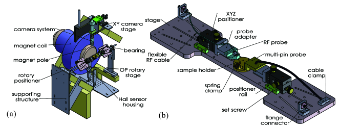
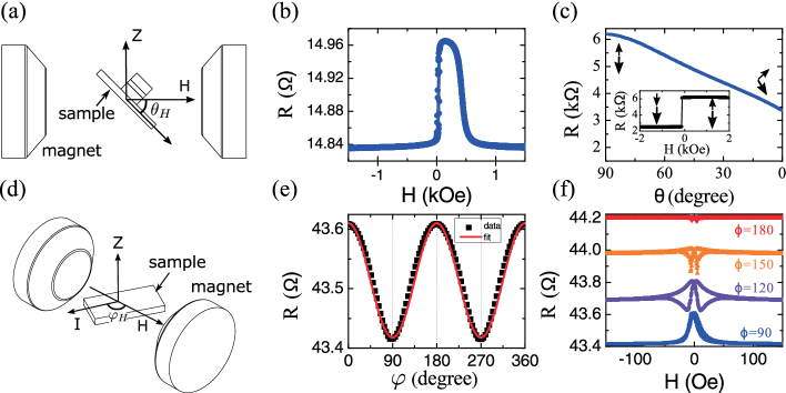
A schematic of the setup with the OP rotary stage installed is shown in Fig. 1 (a). The probe station consists of three main parts: the above mentioned magnet, a vision system and a stage assembly driven by a motorized rotary positioner. Auxiliary parts including supporting structures for the stage and Hall sensor mounting kit are also necessary. The vision system rests on a XY positioner in order to zoom in a device anywhere in a circle of 5 cm diameter. The camera and the lens provide a maximum total magnification of 70. The heavy duty rotary positioner (RM-5 Newmark systems, INC.) has a maximum output torque of 10.2 Nm. One end of the stage was mounted on the positioner and the other end with a guiding tube ran through a bearing. With this configuration, the stage can be oriented with an accuracy of .
Fig. 1 (b) is a closer view of the OP stage. The sample holder with a diameter of 4 cm is equipped with a spring-loaded clip for easy and reliable sample mounting as well as sample position adjustment. The springs are made of BeCu to avoid magnetic impurities. Due to limited space, we used low profile non-magnetic XYZ micro positioners (Quater Research and Development) which have a travel distance of 0.75 cm along each axis. The positioners are partially exposed to the magnetic field. Instead of using vacuum and magnetic mounting base, our positioners were mounted on the stage through rails and locked by set screws. This method improves the stability and allows an additional position adjustment of 2 cm. Up to 4 positioners can be mounted to the stage, which enables a standard four probe low frequency measurement. As can be seen from Fig. 1 (b), probe adapters were used to secure the preferred RF probes and the homemade multi-pin probe. Nonmagnetic flexible RF cables with appropriate length were used. To minimize the vibration of probes due to cable bending, flange connector assemblies and cable clamp at the edge of the stage is crucial. Note that we have minimized the usage of magnetic components for the stage.
The home position of the stage was set for the sample surface parallel to the applied magnetic field. (=0 as illustrated in Fig. 3 (a).) It is necessary to land the probes on the pads (with the guidance of the vision system) at the home position before performing an actual experiment.
II.3 IP rotary stage
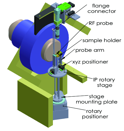
The probe station with the IP rotary stage mounted is shown in Fig. 2. The sample holder placed at the field center, the XYZ micro positioners mounted on the stage and the probes are identical to the ones used in the previous OP stage. The rotary positioner was mounted on a heavy base and the axis of rotation (Z) was aligned to the field center. The circular shape rotary stage, at a height convenient for operating the micro positioners, was mounted through three stainless steel 316 tubes. The probe arm assemblies made of Polyether ether ketone (PEEK) are of essential to reduce the pole gap. Here, with two positioners mounted, the minimum pole gap is 7.5 cm in order to perform an IP rotation. Whenever a RF probe is used, the other end of the RF cable is connected to a RF flange connector fixed at the top of an Al tube. Note that a right angle RF probe (with connector along Z axis which can further reduce the pole gap) is more favorable than the 45 degree probe illustrated in Fig. 2.
III Experimental test and applications
In this section, we present several sets of experimental data to demonstrate the capability of the apparatus. The coordinate system of the probe station is schematically shown in Fig. 3 (a) and (b). is the angle between magnetic field and the sample film plane in a OP rotation whereas corresponds to the angle between the magnetic field and the direction of current flow in an IP rotation.
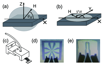
To minimize cable bending in an IP rotation, the rotary stage was configured to rotate between 0 and 180∘. The field polarity is reversed to cover in the range between 180 and 360∘. We assume that the magnetization always follows the orientation of field () in an IP rotation due to the small in plane anisotropy of our samples. Fig. 3 (c) illustrates the film level measurement using a homemade multi-pin probe. Five 45∘ Tungsten needles with 12 m tip diameter were separated by 2 mm. For device level measurement, various probe types such as GSG and ground-signal (GS) RF probes with proper pitch size can be used. Fig. 3 (d) and (e) are two examples using a GSG probe with 250 m pitch size.
III.1 Microwave responses
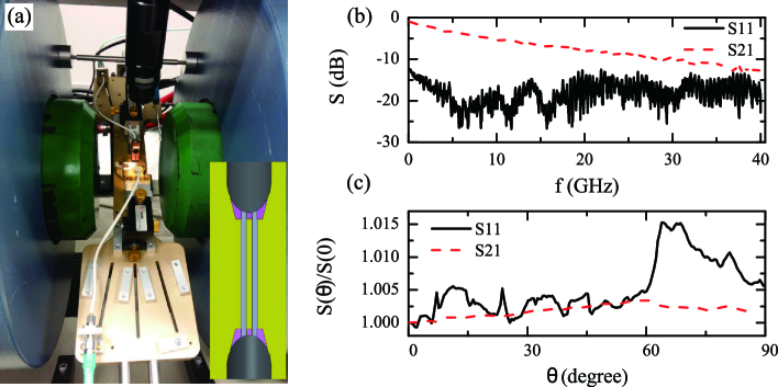
The high frequency responses of the stages including all flexible cables were characterized by a vector network analyzer. The setup configuration of the calibration is shown in Fig. 4 (a). Two-port scattering parameters (S11 and S21 being the reflection coefficient and transmission coefficient, respectively) of the OP rotary stage were measured with a 500 m long coplanar waveguide. The microwave power is 0 dBm. The magnetic field was kept at 2 kOe. Panel (b) is a plot of S11 and S21 as a function of frequency. S21 at 40 GHz is about -12.6 dB which is suitable for techniques such as ferromagnetic resonance(He and Panagopoulos, 2016) and pulse measurements for most magnetic materials. The stage rotation changes the status of cable bending, resulting in a variation in the S parameters. However, as can be seen in Fig. 4 (c), the variation in S parameters between different orientations is normally less than 1. The frequency was fixed at 10 GHz during angle sweep. Similarly, for the IP rotary stage, S11 in ST-FMR configuration only varies about 1 for in the range between 0 and 180 (not shown). Therefore, the rotating stage method causes negligible influence on the data analysis relevant to measurements of the angular dependence.
III.2 DC measurement on films and devices
For DC and low frequency measurements, a Keithley model 6221 current source is used for current injection whereas either a Keithley model 2182A nanovoltmeter or a Stanford Research model SR830 lock in amplifier is used to record the voltage drop across the sample. Fig. 5 (b) is the magnetoresistance (MR) loop taken from a film with stack structure NiTa(150)/Pt(10)/IrMn(8)/Co (3)/Cu(3)/Co(0.5)/CoIr(3)/NiTa(5)/Pt(10) (numbers are nominal thicknesses in nm). The setup configuration using the OP rotary stage is illustrated in Fig. 5 (a). The measurement also requires four adjacent tips of the multi-pin probe as shown in Fig. 3 (c). The data was taken at =0 with a DC current of 1 mA. We observe a sudden resistance jump close to zero field which corresponds to the free layer switch and a broader jump around 500 Oe related to the reference layer switch.(Baibich et al., 1988) A similar MR minor loop on a CoFeB/MgO/CoFeB(Meng et al., 2012) based magnetic tunnel junction (MTJ) device is shown in the inset of Fig. 5 (c). The loop was taken at =90∘ since the device has perpendicular magnetic anisotropy.(Ikeda et al., 2010; Sato et al., 2012) Resistance as a function of field orientation of the MTJ is shown in Fig. 5 (c). The amplitude of the field was 1.5 kOe. Note that the device was originally in the antiparallel high resistance state at =90∘. Both free layer and reference layer were gradually tilted towards the film plane upon changing field orientation, hence the observed decrease in the device resistance. Tilting a free layer is necessary to optimize the performance of a device such as a spin torque diode.(Miwa et al., 2014)
Anisotropy magnetoresistance (AMR) measurement with the IP rotary stage is also easy to perform. Shown in Fig. 5 (e) is an example of a 60 m30 m wide stripe patterned on Py(6 nm)/Pt(10 nm) film. The corresponding measurement configuration is schematically shown in Fig. 5 (d). The field was kept at 1 kOe. Clear oscillation of the resistance as a function of was observed. The solid line is the calculated curve using ,(McGuire and Potter, 1975) where the numbers are the fitting parameters. The fit gives a AMR ratio of =0.45%, smaller than in Py films(Lee et al., 2000) due to the shunting effect of Pt. MR loops of the same device at various field orientations are shown in Fig. 5 (f). Sweeping the magnetic field leads to rotation of the magnetization, which gives rise to the low-field MR and hysteresis. The features, however, are heavily dependent on the field direction which is indicative of magnetic anisotropy,(Fan et al., 2015) including the shape anisotropy of the rectangular stripe.
III.3 Pulse measurement
The bandwidth of the setup depends on the cables and probes being used. The RF cables and probes are suitable for studying the time dependent response of a magnetic device to pulses as short as 50 ps. On the other hand, using the homebuilt multi-pin probes, measurements using pulses in the ~ns range are also possible. A benefit of our design is that up to 10 signal connections are available.
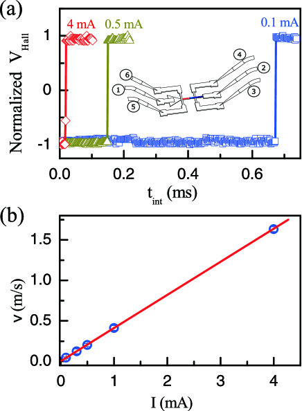
The inset in Fig. 6 (a) shows a schematic of a domain wall motion measurement using pulse current.(Parkin et al., 2008) The stack structure of the 300 nm wide nanowire device is Si/ SiO2/Ta(3)/Pd(3)/[CoFe(0.16)/Pd(0.22)]8/Ta(3), where thehe number in brackets is the thickness of the layers in nm. The nanowire was modified with a triangular contact pad and one Hall cross for magnetotransport measurements. In order to create a single DW in the nanowire, the magnetization of the device was first saturated in one direction using a large positive magnetic field (1 kOe, ). Next, a large pulse current (50 mA, 50 ns) was applied through the Au electrode ( number 5 and 6) to generate a local Oersted field. The DW was then created and pinned at the joint between the triangular contact pad and nanowire.
The DW motion in the nanowire was detected by means of the anomalous Hall effect.(Koyama et al., 2011) CoFe/Pd multilayers exhibit strong perpendicular anisotropy.(Meng et al., 2016) For relatively small magnetic field values in this study, the Hall voltage is nearly proportional to the magnetization at the Hall cross. Therefore, a sudden change in Hall voltage is an indication of magnetization reversal due to domain wall motion. A continuous sine-wave current was injected into the nanowire (electrodes 1 and 2) to measure the Hall resistance through pins 3 and 4 (inset of Fig. 6 (a)). Note that the amplitude ( i=10 A) is too small to drive the DW motion. Two steps are repeated in the measurement. First, a 1 s wide pulse current with desired amplitude from the pulse generator was injected into the nanowire to drive the DW. In a second step, the lock-in amplifier, which was locked to the frequency of i and with a time constant of 0.1 s, was used to measure the Hall resistance (R). Fig. 6 (a) shows R as a function of for three different driving currents. The sudden jump in R is clearly visible , indicating that the DW have passed through the Hall cross due to the spin polarized current. The DW velocity is therefore defined as the distance from the electrode to the Hall cross (30m) divided by the integrated time () of current pulses at which the jump was observed. The extracted averaged DW velocity () as a function of driving current (I) is plotted in Fig. 6 (b). Notably the DW velocity increases linearly with pulse current.
III.4 Spin transfer torque ferromagnetic resonance
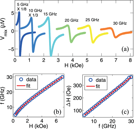
We have also tested our setup with spin transfer torque ferromagnetic resonance (ST-FMR) measurement.(Liu et al., 2011; Wang et al., 2014) The device is the same Py(6 nm)/Pt(10 nm) stripe as for Fig. 5 (c) and (d). The device, as a load, was integrated to a coplanar waveguide of nominal impedance 50 Ohm as shown in Fig. 3 (e). A bias Tee was used to inject the RF current to the device and measure the DC voltage generated in the device simultaneously.(Liu et al., 2011) The microwave output power was kept at 10 dBm while =. Shown in Fig. 7 (a) is the mixing voltage(Liu et al., 2011) as a function of magnetic field for selected microwave frequencies. Resonance peaks are clearly identified up to 30 GHz. All curves are well fitted by the equation:(Liu et al., 2011)
| (1) |
, where and represent the symmetric and antisymmetric Lorentz component of the resonance, respectively. and are the amplitudes of each component. is the resonance field and the full width at half maximum (FWHM) of a resonance spectrum. The fitted parameters are useful for determining important material parameters such as anisotropy and spin Hall angle.(Mellnik et al., 2014; Wang et al., 2014) Shown in Fig. 7 (b) is the Kittel fit to the FMR frequency as a function of resonance magnetic field. For IP magnetic field, , where is the gyromagnetic ratio. The effective magnetization 4=0.82T agrees well with the expected value for Py.(Wang et al., 2014) Furthermore, the linewidth increases linearly with applied microwave frequency as shown in Fig. 7 (c). The damping is obtained by fitting the data to . The relatively large damping coefficient compared to that measured in Permalloy film(Fuchs et al., 2007; He and Panagopoulos, 2016) is attributed to the spin pumping effect due to the thick Pt layer.(Tserkovnyak et al., 2002)
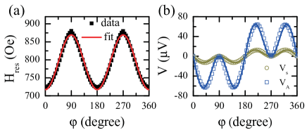
Compared to the measurement at a fixed angle, we are more interested in the angular dependence of the ST-FMR spectrum. Fig. 8 shows the IP angular dependence of the resonance field and resonance amplitudes measured at 8 GHz. The data points are extracted by fitting 72 spectra collected at a list of field orientations. For this particular sample, besides the perpendicular uniaxial anisotropy which is included in , an additional in-plane uniaxial anisotropy (effective field ) with easy axis along the long-side is assumed. Using the coordinates defined in Fig. 3, the resonance condition for any given IP field orientation can be derived:(Maksymowicz and Leaver, 1973; Liu et al., 2003)
| (2) |
Thus, =0.84T and =622 Oe . Py/Pt is a well investigated bilayer for the spin Hall effect (SHE).(Sinova et al., 2015) The antisymmetric and symmetric voltage components are attributed to field-like torque and spin torque generated by the SHE, respectively. The output DC voltages arise from the combined effect of AMR and magnetization precession driven by these torques.(Azevedo et al., 2011) A relation is expected if no other effect is involved.(Harder et al., 2011; Skinner et al., 2014; Mecking et al., 2007) As can be seen in Fig. 8 (b), both components can be fitted well by this relation, adding credence to the suitability of the IP rotary stage for angular dependent studies. Note that the measurement only takes 4 h with a single program sequence. In contrast, using probe stations equipped with rotary sample stages, each data point shown in Fig. 8 requires a separate probe landing and stage rotating procedures. It can take several days to obtain the same curve. Therefore, the method of rotating sample and probes simultaneously is much more efficient.
IV conclusion
We have developed a probe station to study magnetic films and devices with controllable field orientation. The sample holder, probe assembly and microwave cables are rotated simultaneously with two separate motorized stages. The sample rotation is equivalent to a field rotation which covers from 0 to and from 0 to . We have also shown novel designs of a vision system assembly, sample holder with spring-loaded clip, micro positioner mounting and multi-pin probe. Furthermore, a range of DC and RF measurement techniques incorporated to this probe station were employed to demonstrate the versatility of this probe station. The angular-resolved RF probe station is useful for determining magnetic anisotropy, evaluating device performance and addressing the physics of spin torque.
Acknowledgements.
The authors are grateful to Yi Wang, Sze Ter Lim, Cheow Hin Sim and Ruisheng Liu for fruitful discussions. We thank HongJing Chung for preparing films. We acknowledge Singapore Ministry of Education (MOE), Academic Research Fund Tier 2 (Reference No: MOE2014-T2-1-050) and National Research Foundation (NRF) of Singapore, NRF-Investigatorship (Reference No: NRF-NRFI2015-04) for the funding of this research.References
- Slonczewski (1996) J. C. Slonczewski, Journal of Magnetism and Magnetic Materials 159, L1 (1996).
- Mangin et al. (2006) S. Mangin, D. Ravelosona, J. A. Katine, M. J. Carey, B. D. Terris, and E. E. Fullerton, Nat Mater 5, 210 (2006).
- Rippard et al. (2004) W. H. Rippard, M. R. Pufall, S. Kaka, S. E. Russek, and T. J. Silva, Physical Review Letters 92, 027201 (2004).
- Houssameddine et al. (2007) D. Houssameddine, U. Ebels, B. Delaet, B. Rodmacq, I. Firastrau, F. Ponthenier, M. Brunet, C. Thirion, J. P. Michel, L. Prejbeanu-Buda, M. C. Cyrille, O. Redon, and B. Dieny, Nat Mater 6, 441 (2007).
- Ikeda et al. (2010) S. Ikeda, K. Miura, H. Yamamoto, K. Mizunuma, H. D. Gan, M. Endo, S. Kanai, J. Hayakawa, F. Matsukura, and H. Ohno, Nat Mater 9, 721 (2010).
- Liu et al. (2012) L. Liu, C.-F. Pai, Y. Li, H. W. Tseng, D. C. Ralph, and R. A. Buhrman, Science 336, 555 (2012).
- Yu et al. (2014) G. Yu, P. Upadhyaya, Y. Fan, J. G. Alzate, W. Jiang, K. L. Wong, S. Takei, S. A. Bender, L.-T. Chang, Y. Jiang, M. Lang, J. Tang, Y. Wang, Y. Tserkovnyak, P. K. Amiri, and K. L. Wang, Nat Nano 9, 548 (2014).
- (8) See http://www.gmw.com/electromagnets/Miniature/5201/5201.html.
- Li et al. (2012) J. Li, E. Jin, H. Son, A. Tan, W. N. Cao, C. Hwang, and Z. Q. Qiu, Review of Scientific Instruments 83, 033906 (2012).
- (10) See http://www.lakeshore.com/products/Cryogenic-Probe-Stations/Pages/Cryogenic-Probe-Stations.aspx.
- (11) See http://www.janis.com/NewsandEvents/PressReleases/200906.aspx.
- Mellnik et al. (2014) A. R. Mellnik, J. S. Lee, A. Richardella, J. L. Grab, P. J. Mintun, M. H. Fischer, A. Vaezi, A. Manchon, E. A. Kim, N. Samarth, and D. C. Ralph, Nature 511, 449 (2014).
- Wang et al. (2014) Y. Wang, P. Deorani, X. Qiu, J. H. Kwon, and H. Yang, Applied Physics Letters 105, 152412 (2014).
- He and Panagopoulos (2016) S. He and C. Panagopoulos, Review of Scientific Instruments 87, 043110 (2016).
- Baibich et al. (1988) M. N. Baibich, J. M. Broto, A. Fert, F. N. Van Dau, F. Petroff, P. Etienne, G. Creuzet, A. Friederich, and J. Chazelas, Phys. Rev. Lett. 61, 2472 (1988).
- Meng et al. (2012) H. Meng, R. Sbiaa, M. A. K. Akhtar, R. S. Liu, V. B. Naik, and C. C. Wang, Applied Physics Letters 100, 122405 (2012).
- Sato et al. (2012) H. Sato, M. Yamanouchi, S. Ikeda, S. Fukami, F. Matsukura, and H. Ohno, Applied Physics Letters 101, 022414 (2012).
- Miwa et al. (2014) S. Miwa, S. Ishibashi, H. Tomita, T. Nozaki, E. Tamura, K. Ando, N. Mizuochi, T. Saruya, H. Kubota, K. Yakushiji, T. Taniguchi, H. Imamura, A. Fukushima, S. Yuasa, and Y. Suzuki, Nat Mater 13, 50 (2014).
- McGuire and Potter (1975) T. McGuire and R. Potter, IEEE Transactions on Magnetics 11, 1018 (1975).
- Lee et al. (2000) W. Y. Lee, M. F. Toney, and D. Mauri, IEEE Transactions on Magnetics 36, 381 (2000).
- Fan et al. (2015) X. Fan, H. Zhou, J. Rao, X. Zhao, J. Zhao, F. Zhang, and D. Xue, Scientific Reports 5, 16139 (2015).
- Parkin et al. (2008) S. S. P. Parkin, M. Hayashi, and L. Thomas, Science 320, 190 (2008).
- Koyama et al. (2011) T. Koyama, D. Chiba, K. Ueda, K. Kondou, H. Tanigawa, S. Fukami, T. Suzuki, N. Ohshima, N. Ishiwata, Y. Nakatani, K. Kobayashi, and T. Ono, Nat Mater 10, 194 (2011).
- Meng et al. (2016) Z. Meng, S. He, J. Qiu, T. Zhou, G. Han, and K.-L. Teo, Journal of Applied Physics 119, 083905 (2016).
- Liu et al. (2011) L. Liu, T. Moriyama, D. C. Ralph, and R. A. Buhrman, Phys. Rev. Lett. 106, 036601 (2011).
- Fuchs et al. (2007) G. D. Fuchs, J. C. Sankey, V. S. Pribiag, L. Qian, P. M. Braganca, A. G. F. Garcia, E. M. Ryan, Z.-P. Li, O. Ozatay, D. C. Ralph, and R. A. Buhrman, Applied Physics Letters 91, 062507 (2007).
- Tserkovnyak et al. (2002) Y. Tserkovnyak, A. Brataas, and G. E. W. Bauer, Physical Review Letters 88, 117601 (2002).
- Maksymowicz and Leaver (1973) A. Z. Maksymowicz and K. D. Leaver, Journal of Physics F: Metal Physics 3, 1031 (1973).
- Liu et al. (2003) X. Liu, Y. Sasaki, and J. K. Furdyna, Physical Review B 67 (2003).
- Sinova et al. (2015) J. Sinova, S. O. Valenzuela, J. Wunderlich, C. H. Back, and T. Jungwirth, Reviews of Modern Physics 87, 1213 (2015).
- Azevedo et al. (2011) A. Azevedo, L. H. Vilela-Leão, R. L. Rodríguez-Suárez, A. F. Lacerda Santos, and S. M. Rezende, Physical Review B 83, 144402 (2011).
- Harder et al. (2011) M. Harder, Z. X. Cao, Y. S. Gui, X. L. Fan, and C. M. Hu, Physical Review B 84, 054423 (2011).
- Skinner et al. (2014) T. D. Skinner, M. Wang, A. T. Hindmarch, A. W. Rushforth, A. C. Irvine, D. Heiss, H. Kurebayashi, and A. J. Ferguson, Applied Physics Letters 104, 062401 (2014).
- Mecking et al. (2007) N. Mecking, Y. S. Gui, and C.-M. Hu, Phys. Rev. B 76, 224430 (2007).