Transparent Semiconductor-Superconductor Interface and Induced Gap
in an Epitaxial Heterostructure Josephson Junction
Abstract
Measurement of multiple Andreev reflection (MAR) in a Josephson junction made from an InAs heterostructure with epitaxial aluminum is used to quantify the highly transparent semiconductor-superconductor interface, indicating near-unity transmission. The observed temperature dependence of MAR does not follow a conventional BCS form, but instead agrees with a model in which the density of states in the quantum well acquires an effective induced gap, in our case , close to that of the epitaxial superconductor. Carrier density dependence of MAR is investigated using a depletion gate, revealing the subband structure of the semiconductor quantum well, consistent with magnetotransport experiment of the bare InAs performed on the same wafer.
Increasing interest in the superconducting proximity effect in semiconductors arises from recent proposals to realize hybrid topological materials for quantum information processing Alicea et al. (2011); Leijnse and Flensberg (2011); Aasen et al. (2015). For this application, the quality of the superconductor-semiconductor interface, which controls how superconducting properties are imparted on the semiconductor, is of critical importance Blonder et al. (1982); Takei et al. (2013); Cole et al. (2015). From another perspective, many ballistic and mesoscopic transport effects are expected in semiconductor-superconductor hybrids Beenakker (1991, 1992) have not been investigated due to lack of an appropriate material system. Hybrid systems consisting of a superconducting metal in contact with a two-dimensional electron gas (2DEG) were widely explored in previous decades Takayanagi et al. (1995a, b); Chrestin et al. (1997); Bauch et al. (2005), but material difficulties hampered progress Mur et al. (1996); Giazotto et al. (2004); Bauch et al. (2005); Amado et al. (2013).
In semiconductor nanowires, the difficulty of creating strong uniform coupling to a superconductor was recently resolved by growing the superconductor material in situ by molecular beam epitaxy Krogstrup et al. (2015). A hard superconducting gap, measured by tunneling into the wire end, indicated an intimate coupling between materials Chang et al. (2015). More recently, in situ growth of Al has been applied to InAs 2DEGs Shabani et al. (2016). This system also exhibits a hard superconducting gap in tunnel spectroscopy Kjaergaard et al. (2016).
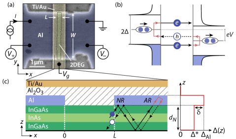
In this work, we report multiple Andreev reflection (MAR) in a gateable Josephson junction formed from an InAs 2DEG/epitaxial Al heterostructure. We observe a temperature dependence of the MAR peak positions that differs from expectations for a conventional BCS-like gap, but is consistent with an induced gap in the InAs under the Al Aminov et al. (1996); Takei et al. (2013); Cole et al. (2015); Reeg and Maslov (2016). The appearance of an induced gap, , in the local density of states of the semiconductor reflects the finite time a state from the quantum well spends in the superconductor Golubov and Kupriyanov (1996). Comparing MAR data to a quantitative model (described below), we infer an induced gap and a transmission between the gapped and ungapped InAs regions in excess of . These results are consistent with tunnel spectroscopy measurements on the same wafer Kjaergaard et al. (2016).
The high transparency of our junction is further confirmed by the shape of MAR features appearing as peaks in resistance, rather than the more commonly observed peaks in conductance, when the voltage is tuned to . This dip-to-peak transition is a longstanding prediction for highly transparent junctions Averin and Bardas (1995), also confirmed by our quantitative modeling. To our knowledge, this inversion has not be reported in the experimental literature, even for junctions considered highly transparent (see, for instance, Ref. Doh et al. (2005); Xiang et al. (2006); Li et al. (2016)). We discuss the dip-to-peak transition further in the Supplemental Material sup .
Modeling also reveals the existence of two distinct families of MAR resonances at zero top-gate voltage, which we associate with two occupied subbands in the 2DEG. By energizing a top gate on the exposed 2DEG, the resonant features change, becoming consistent with single-subband occupancy. The gate-dependent change from two to one subband is consistent with magnetotransport measurements on a Hall bar with the Al removed, fabricated on the same wafer.
The hybrid heterostructure was grown by molecular beam epitaxy, and consists (from top to bottom) of 10 nm Al, 10 nm In0.81Ga0.19As, 7 nm InAs (quantum well), 4 nm In0.81Ga0.19, and an InAlAs buffer on an InP wafer. We emphasize that the Al layer is grown in situ as part of the heterostructure Shabani et al. (2016). Density and mobility , measured in a top-gated Hall bar geometry with the Al removed, yield a mean free path at top-gate voltage . As demonstrated below, at the quantum well has two subbands occupied (see also Supplementary Material sup ).
The wafer is patterned into mesa structures using a standard III-V wet etch. The Al is then patterned using a selective Al etch (Transene D). Next, an unpatterned nm aluminum oxide layer is deposited using atomic layer deposition. Finally, a Ti/Au gate is deposited, patterned to cover the exposed 2DEG. Figure 1a shows a false-color scanning electron micrograph of the final device, and Fig. 1c shows a schematic cross-section through the junction. The exposed 2DEG region has a length and a width . The superconducting gap of the 10 nm thick Al layer is inferred from the critical temperature (, independently measured in four-terminal measurement) via . We note that the gap of the Al layer is larger than bulk Al Merservey and Schwartz (1969), with a consistent with previously reported values Meservey and Tedrow (1971); Court et al. (2008).
All measurements were performed in a dilution refrigerator with base temperature using standard DC and lockin techniques, with current excitation in the range 2.5 nA to 5 nA.
The theoretical approach to this system begins with the Octavio-Blonder-Tinkham-Klapwijk (OBTK) model for multiple Andreev reflections Octavio et al. (1983). As originally formulated, this model assumes a well-defined voltage is dropped across the normal region (green rectangle in Fig. 1a), leading to the MAR process sketched in Fig. 2b. For a planar junction where the 2DEG extends under the Al (Fig. 1c), the voltage can also drop along the horizontal Al-2DEG interface. In the case of imperfect Al-2DEG transparency, this leads to smearing of the resonances arising from MAR Kleinsasser et al. (1990); Nitta et al. (1992). The OBTK model was later extended to account for the planar geometry Aminov et al. (1996), denoted SNcNS, where is the semiconducting region in which the superconducting top layer has been removed. The SN electrodes, consisting of 2DEG with Al on top, are assumed to be disordered and in equilibrium, while the exposed 2DEG region of length is assumed ballistic. The model yields a renormalized density of states in the 2DEG, with an induced gap, determined by the quality of the interface between the 2DEG and the Al Aminov et al. (1996).
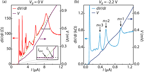
Figure 2 shows differential resistance (left) and DC voltage (right), as a function of applied DC current, for two gate voltages. The inset in Fig. 2a show a zoom-in indicating the excess current and critical current for . The critical current is yielding an product of , about 70% of the gap of the Al film, and a critical current density . The excess current, reflecting enhanced current through the junction due to Andreev reflection, is defined as the intercept of a linear fit to taken at (green dashed line in Fig. 2a). The measured excess current, , corresponds to 111The excess current is related to the gap via , where in the ballistic, fully transparent case Blonder et al. (1982), and in the diffusive case Artemenko et al. (1979).. The differential resistance (red curve in Fig. 2a) shows a series of peaks as the current is increased. The peak/dip structure is a manifestation of the MAR processes and is expected to follow the series , with corresponding to the number of Andreev reflections.
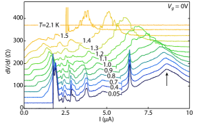
However, the broad resistance peak, highlighted with black horizontal bar in Fig. 2a, occurs at energies larger than but follows the temperature dependence of and disappears at (see Supplemental Material sup ), indicating that the feature has a superconductive origin. Such anomalous resistance features are believed to be associated with the planar Josephson junction geometry Nguyen et al. (1992, 1994), where quasiparticles in the 2DEG can undergo several scattering events at the Al interface before ultimately undergoing Andreev reflection and traversing the same path back. An example of such a process is sketched in Fig. 1c. On a length scale smaller than the normal-state coherence length , this process will appear as Andreev reflection from an effective boundary, indicated by the white dashed line in Fig. 1c. The finite-bias properties of such systems cannot be adequately described by either the SNcNS or OBTK models, and the simple picture in Fig. 1b breaks down. With the contacts out of equilibrium, the position of the peaks in Fig. 2a cannot be directly related to the superconducting gap. However, by increasing the resistance in the exposed region relative to the horizontal interface, the peaks at finite-bias follow a regular series and can be used to extract a value for the induced gap.
In Fig. 2b, the gate covering the exposed 2DEG region is energized to , substantially depleting the junction, leading to a normal state resistance . At this gate voltage, the broad resistance peak at energy is absent, and the DC voltages of the first three peaks (indicated with vertical black arrows) are positioned proportional to , indicating that the voltage drop now occurs predominantly in the uncovered 2DEG region. At this gate voltage is reduced from the value (full versus given in Supplementary Material sup ). As we show below, the curves in Fig. 2 are consistent with near unity transmission through the junction. In such transparent junctions, the peaks due to MAR resonances appear in the differential resistance, as opposed to peaks in the differential conductance sup . The vertical arrows in Fig. 2b therefore point to peaks in resistance, not in conductance, to indicate multiples of the gap, arising from the relation
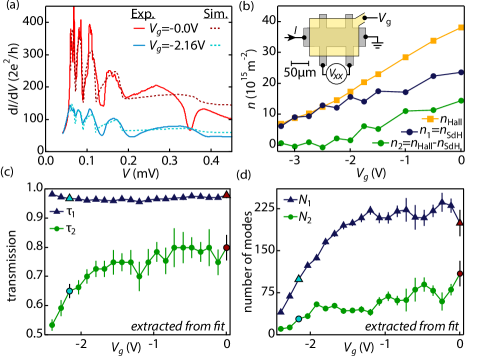
To extract the value of , we plot the conductance from Fig. 2 against the DC voltage drop, as shown in Fig. 3a. The theoretical MAR resonances in Fig. 3a are simulated using a generalized scattering matrix approach developed for SNS junctions Averin and Bardas (1995); Bratus et al. (1995). Within the model of an induced gap Aminov et al. (1996) the SNcNS system is interpreted as an effective SNS∗-junction, where is the superconducting quantum well with a gap and a critical temperature identical to that of the parent superconductor. Simulations are performed by calculating the conductance of a single mode with transmission , from the DC component of the current . The time-independent Fourier component of is calculated from the wave functions of the quasiparticles accelerated by the voltage across the junction. In the case of a ballistic junction (), the back-scattering effectively only occurs at the boundary between and (dashed white line in Fig. 1c). The total current through the junction is the sum of currents carried by modes in subbands. The resulting conductance through the multimode junction is given by where is the number of modes in the ’th subband, and is the transmission of the modes in the ’th subband.
A nonlinear least-squares procedure is used to fit simulated curves to the data in Fig. 3b, where and are fitting parameters and is predefined (see also Allen et al. (2015)). The minimal number of subbands needed to capture the essential features of the data was found to be . For the optimal fit did not populate the subbands (i.e. for ), indicating that the data is well described by two subbands (in Supplementary Material we present simulations using and sup ). The result of fitting to the MAR features at two values are shown as dashed curves in Fig. 3a. At , the induced gap was with , , , and . When the gate is energized to the fitting values are , with , , , and . The gate-voltage dependence of the fitting parameters and are shown in Figs. 3c and 3d. The gap extracted from the fitting routine is identical to the one measured in a tunneling experiment on the same wafer Kjaergaard et al. (2016).
The presence of two transmission species in the optimal fit is attributed to the 2DEG having two occupied subbands. The carrier density in the 2DEG, denoted , is measured in a Hall bar geometry via the Hall slope (shown in Fig. 3b). The density from the Hall slope is compared to the density extracted from the periodicity of the SdH oscillations in an out-of-plane magnetic field. The data in Fig. 3b show the density change in the 2DEG as the top gate is energized. The power spectrum of exhibit a two peak structure, indicating two subbands with different densities in the quantum well at Averkiev et al. (2001). The density corresponding to the major peak is denoted , and the difference is denoted . The density in the two subbands changes as the topgate is energized, as shown in Fig. 3b, similar to and extracted from fitting to the MAR features. In particular, the species becomes depopulated at a gate voltage similar to the depletion of the second subband in the Hall bar (Fig. 3b). The decrease of transmission of the species in Fig. 3c could be due to a breakdown of the ballistic assumption as the second subband is depleted.
Within the 1D Blonder-Tinkham-Klapwijk (BTK) formalism for an SN interface, the transparency is often parametrized using the dimensionless quantity , related to the transmission via Blonder et al. (1982). For the first subband we extract an average transmission , corresponding to a -parameter of , indicating a near pristine effective interface for this mode, between the uncovered and Al-covered regions of the 2DEG in this system.
The distinction between a BCS-like gap, , and an induced gap, , is revealed through the temperature dependence of the superconducting properties. In the case where the effective thickness of the quantum well is much less than the normal-state coherence length, , any position-dependence of the gap magnitude in the growth direction in the 2DEG can be neglected, and the temperature dependence of the induced gap depends on according to Volkov et al. (1995); Aminov et al. (1996); Chrestin et al. (1997)
| (1) |
where is determined self-consistently from BCS theory. The dimensionless parameter is a measure of the horizontal SN interface transparency, where corresponds to a perfectly transparent interface Schäpers (2001). The parameter represents the discontinuity in the superconducting pair-potential and gives rise to the difference between the gap in aluminum, , and the induced gap, , in the 2DEG, denoted in Fig. 1c. For the present case we find , using and , consistent with a high quality interface between the semiconductor and Al.
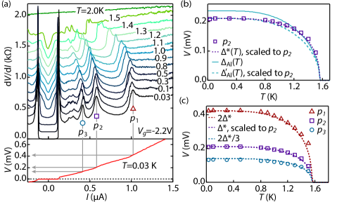
To elucidate the nature of the induced superconducting gap, we study the temperature dependence of the differential resistance at , shown in Fig. 4a. The position of the second MAR related peak (denoted ) is tracked in Fig. 4b as the temperature is increased. The curves in Fig. 4b show the solution of Eq. (1) (purple), temperature dependence of a BCS gap, , (teal), and a BCS-like gap, , (teal, dashed), where the gap value has been rescaled to coincide with the data at . The inadequacy of the temperature dependence of a BCS-like gap (both unscaled and rescaled) to account for the temperature dependence of the peaks is contrasted by the good correspondence between Eq. (1) and our data. The temperature dependence of the first and third peak positions, and , are shown in Fig. 4c. The curves identified with and are found by multiplying by a factor of 2 and 2/3, respectively, corresponding to and in the MAR series. We note that in the case of a highly transmissive junction the position of the maximum related to the MAR resonance is not located exactly at sup . The excellent agreement also with and resonances indicate that the superconducting properties of the junction are well described within the induced gap model.
In conclusion, we have measured MAR resonances in a Josephson junction in a InAs 2DEG heterostructure, where aluminum is epitaxially matched to the 2DEG. By fitting the conductance of the MAR features, we extract a transmission close to unity through an effective SNS∗-junction, where S∗ represents the InAs quantum well covered by the Al. The temperature dependence of the MAR resonances is well-described by the theory of an effective induced gap, and we find in the Al covered 2DEG region.
Acknowledgements: The authors acknowledge enlightening discussions with K. Flensberg. Research support by Microsoft Research and the Danish National Research Foundation. C.M.M. acknowledges support from the Villum Foundation. F.N. acknowledges support from a Marie Curie Fellowship (No. 659653). M.P.N. acknowledges support from ERC Synergy Grant. A.A. is supported by an ERC Starting Grant, the Foundation for Fundamental Research on Matter (FOM) and the Netherlands Organization for Scientific Research (NWO/OCW) as part of the Frontiers of Nanoscience program.
References
- Alicea et al. (2011) J. Alicea, Y. Oreg, G. Refael, F. von Oppen, and M. P. A. Fisher, Nature Physics 7, 412 (2011).
- Leijnse and Flensberg (2011) M. Leijnse and K. Flensberg, Phys. Rev. Lett. 107, 210502 (2011).
- Aasen et al. (2015) D. Aasen, M. Hell, R. V. Mishmash, A. Higginbotham, J. Danon, M. Leijnse, T. S. Jespersen, J. A. Folk, C. M. Marcus, K. Flensberg, and J. Alicea, ArXiv e-prints (2015), arXiv:1511.05153 .
- Blonder et al. (1982) G. E. Blonder, M. Tinkham, and T. Klapwijk, Phys. Rev. B 25, 4515 (1982).
- Takei et al. (2013) S. Takei, B. M. Fregoso, H.-Y. Hui, A. M. Lobos, and S. Das Sarma, Phys. Rev. Lett. 110, 186803 (2013).
- Cole et al. (2015) W. S. Cole, S. Das Sarma, and T. D. Stanescu, Phys. Rev. B 92, 174511 (2015).
- Beenakker (1991) C. W. J. Beenakker, Phys. Rev. Lett. 67, 3836 (1991).
- Beenakker (1992) C. W. J. Beenakker, Phys. Rev. B 46, 12841 (1992).
- Takayanagi et al. (1995a) H. Takayanagi, J. B. Hansen, and J. Nitta, Phys. Rev. Lett. 74, 166 (1995a).
- Takayanagi et al. (1995b) H. Takayanagi, T. Akazaki, and J. Nitta, Phys. Rev. Lett. 75, 3533 (1995b).
- Chrestin et al. (1997) A. Chrestin, T. Matsuyama, and U. Merkt, Phys. Rev. B 55, 8457 (1997).
- Bauch et al. (2005) T. Bauch, E. Hürfeld, V. Krasnov, P. Delsing, H. Takayanagi, and T. Akazaki, Phys. Rev. B 71, 174502 (2005).
- Mur et al. (1996) L. C. Mur, C. Harmans, J. E. Mooij, J. F. Carlin, and A. Rudra, Phys. Rev. B 54, R2327 (1996).
- Giazotto et al. (2004) F. Giazotto, K. Grove-Rasmussen, R. Fazio, F. Beltram, E. H. Linfield, and D. A. Ritchie, Journal of Superconductivity 17, 317 (2004).
- Amado et al. (2013) M. Amado, A. Fornieri, F. Carillo, G. Biasiol, L. Sorba, V. Pellegrini, and F. Giazotto, Phys. Rev. B 87, 134506 (2013).
- Krogstrup et al. (2015) P. Krogstrup, N. L. B. Ziino, W. Chang, S. M. Albrecht, M. H. Madsen, E. Johnson, J. Nygård, C. M. Marcus, and T. S. Jespersen, Nature Materials 14, 400 (2015).
- Chang et al. (2015) W. Chang, S. M. Albrecht, T. S. Jespersen, F. Kuemmeth, P. Krogstrup, J. Nygård, and C. M. Marcus, Nature Nanotechnology 10, 232 (2015).
- Shabani et al. (2016) J. Shabani, M. Kjaergaard, H. J. Suominen, Y. Kim, F. Nichele, K. Pakrouski, T. Stankevic, R. M. Lutchyn, P. Krogstrup, R. Feidenhans’l, S. Kraemer, C. Nayak, M. Troyer, C. M. Marcus, and C. J. Palmstrøm, Phys. Rev. B 93, 155402 (2016).
- Kjaergaard et al. (2016) M. Kjaergaard, F. Nichele, H. J. Suominen, M. P. Nowak, M. Wimmer, A. R. Akhmerov, J. A. Folk, K. Flensberg, J. Shabani, C. J. Palmstrøm, and C. M. Marcus, ArXiv e-prints (2016), arXiv:1603.01852 .
- Aminov et al. (1996) B. A. Aminov, A. A. Golubov, and M. Y. Kupriyanov, Phys. Rev. B 53, 365 (1996).
- Reeg and Maslov (2016) C. R. Reeg and D. L. Maslov, ArXiv e-prints (2016), arXiv:1603.03354 .
- Golubov and Kupriyanov (1996) A. A. Golubov and M. Y. Kupriyanov, Physica C 259, 27 (1996).
- Averin and Bardas (1995) D. Averin and A. Bardas, Phys. Rev. Lett. 75, 1831 (1995).
- Doh et al. (2005) Y.-J. Doh, J. A. van Dam, A. L. Roest, E. P. A. M. Bakkers, L. P. Kouwenhoven, and S. De Franceschi, Science 309, 272 (2005).
- Xiang et al. (2006) J. Xiang, A. Vidan, M. Tinkham, R. M. Westervelt, and C. M. Lieber, Nature Nanotechnology 1, 208 (2006).
- Li et al. (2016) S. Li, N. Kang, D. X. Fan, L. B. Wang, Y. Q. Huang, P. Caroff, and H. Q. Xu, Scientific Reports 6, 24822 (2016).
- (27) See Supplemental Material at [URL] for additional data and numerical simulations .
- Merservey and Schwartz (1969) R. Merservey and B. B. Schwartz, Superconductivity Vol. 1, edited by R. D. Parks (Marcel Dekker Inc., 1969).
- Meservey and Tedrow (1971) R. Meservey and P. M. Tedrow, Journal of Applied Physics 42 (1971).
- Court et al. (2008) N. A. Court, A. J. Ferguson, and R. G. Clark, Superconductor Science and Technology 21, 015013 (2008).
- Octavio et al. (1983) M. Octavio, M. Tinkham, G. E. Blonder, and T. Klapwijk, Phys. Rev. B 27, 6739 (1983).
- Kleinsasser et al. (1990) A. W. Kleinsasser, T. N. Jackson, D. McInturff, F. Rammo, G. D. Pettit, and J. M. Woodall, Appl. Phys. Lett. 57, 1811 (1990).
- Nitta et al. (1992) J. Nitta, T. Akazaki, H. Takayanagi, and K. Arai, Phys. Rev. B 46, 14286 (1992).
- Note (1) The excess current is related to the gap via , where in the ballistic, fully transparent case Blonder et al. (1982), and in the diffusive case Artemenko et al. (1979).
- Nguyen et al. (1992) C. Nguyen, H. Kroemer, and E. L. Hu, Phys. Rev. Lett. 69, 2847 (1992).
- Nguyen et al. (1994) C. Nguyen, H. Kroemer, and E. L. Hu, Applied Physics Letters 65 (1994).
- Bratus et al. (1995) E. N. Bratus, V. S. Shumeiko, and G. Wendin, Phys. Rev. Lett. 74, 2110 (1995).
- Allen et al. (2015) M. T. Allen, O. Shtanko, I. C. Fulga, J. I.-J. Wang, D. Nurgaliev, K. Watanabe, T. Taniguchi, A. R. Akhmerov, P. Jarillo-Herrero, L. S. Levitov, and A. Yacoby, ArXiv e-prints (2015), arXiv:1506.06734 [cond-mat.mes-hall] .
- Averkiev et al. (2001) N. S. Averkiev, L. E. Golub, S. A. Tarasenko, and M. Willander, Journal of Physics: Condensed Matter 13, 2517 (2001).
- Volkov et al. (1995) A. F. Volkov, P. H. C. Magnée, B. J. Van Wees, and T. M. Klapwijk, Physica C: Superconductivity 242, 261 (1995).
- Schäpers (2001) T. Schäpers, Superconductor/Semiconductor Junctions, Springer Tracts in Modern Physics, Vol. 174 (Springer, Berlin, Heidelberg, 2001).
- Artemenko et al. (1979) S. N. Artemenko, A. F. Volkov, and A. V. Zaitsev, Solid State Communications 30, 771 (1979).
Supplementary material for “Transparent Semiconductor-Superconductor Interface and Induced Gap in an Epitaxial Heterostructure Josephson Junction”
Mobility peak and Shubnikov-de Haas oscillations
In Fig. S1a the gate-dependence of the 2DEG mobility is shown, measured in the same Hall bar as the data in Fig. 3b of the main paper. The mobility peak is at , the same gate-voltage value at which (see Fig. 3b), consistent with the interpretation of a mobility-limiting second subband being depleted. Two examples Shubnikov-de Haas oscillations of is shown in Fig. S1b, at (the two subband regime) and (the one subband regime).

Gate dependence of the superconducting properties of the 2DEG
The gate-voltage dependence of the differential resistance of the S-2DEG-S junction is shown in Fig. S2. At the junction is no longer able to sustain a supercurrent, and the normal state resistance is . The product is only slightly gate-voltage dependent (Fig. S2b), with a maximum at .

Temperature dependence of the anomalous resistance peak
Figure S3 shows the evolution of the differential resistance, as the temperature is increased at . The anomalous resistance peak in the differential resistance (highlighted with vertical black arrow) has identical temperature dependence to other superconducting features of the device. The complementary data at is shown in Fig. 4 of the main paper.
MAR signatures in junctions with transmission close to unity
In highly transparent junctions, the curves are qualitatively different from the opaque situation. In general, the current is a combination of the number of Andreev reflections, , and the transmission of the junction. For the ’th order Andreev reflection, the particle traverses the normal region times, and neglecting the energy dependence of Andreev reflection probability, the current will depend on transmission as,
| (S1) |
For low , the current thus decreases rapidly for higher order Andreev reflection processes (i.e. increasing ). In contrast, for very transparent interfaces, higher order Andreev reflections will still yield an appreciable contribution to the current. This situation is demonstrated in Fig. S4a, where we show the current in an SNS device, calculated according to Eq. S1. For low transparencies, the slope of the versus curves increases as decreases and the current is increased at the transition from to Andreev reflections. As a result, the conductance of opaque junctions forms a staircase-pattern that increases in voltage with peaks at the subgap features (cf. the conductance depicted with the blue and green curves in Fig. S4b, calculated using the model of Ref. Averin and Bardas (1995)). In contrast, in the transmissive junctions, the current curve exhibits an opposite pattern, which results in a declining staircase-pattern in the conductance with the peaks replaced by dips (see the purple curve in Fig. S4b). This leads to an overall increase in the conductance between values of the voltage corresponding to integer multiples of the gap (i.e. at ).

In Fig. 4 of the main paper the peaks in differential resistance (labeled with , and ) of the MAR are tracked as the temperature is increased. The energy corresponding to the second peak in the differential resistance is not identical to the value of the gap, as shown in Fig. S4b, where the position of the resistance peak associated with the MAR reflection is indicated by the vertical black arrow. As the transparency is increased, the peak in resistance moves further away from integer multiples of the gap. From the simulation in Fig. S4b the difference between the position of and the value of the gap is at . In the main text the value of is while in reasonable agreement with the difference. The correspondence between the temperature dependence of MAR features and temperature dependence of the gap is unchanged by this effect.
Subbands in the simulations
In the main article we introduce the simulations used to fit the MAR features, in Fig. 3a. The fit procedure takes as input a fixed number of subbands, denoted , which can have a different number of modes, , and transmission . At we find the optimal subband number is .
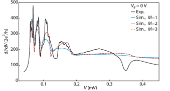
As shown in Fig. S5 at the fit is visibly worse, while for the optimal least-squares fit to the experimental data does not involve any modes in the third subband, i.e. . We note, that for and a specific choice of the initial guess of the parameters, the fitting procedure can distribute modes among all three subbands, creating two subbands that are almost degenerate in transmission probability. When this happens the fitting errors of and are larger than the fitted values by several orders of magnitude, and hence we disregard such solutions. In Table 1 we list the number of modes in the optimal least-squares fit, for .
|
|