.tifpng.pngconvert #1 \OutputFile \AppendGraphicsExtensions.tif
Surface state dominated spin-charge current conversion in topological insulator/ferromagnetic insulator heterostructures
Abstract
We report the observation of ferromagnetic resonance-driven spin pumping signals at room temperature in three-dimensional topological insulator thin films – Bi2Se3 and (Bi,Sb)2Te3 – deposited by molecular beam epitaxy on Y3Fe5O12 thin films. By systematically varying the Bi2Se3 film thickness, we show that the spin-charge conversion efficiency, characterized by the inverse Rashba-Edelstein effect length (), increases dramatically as the film thickness is increased from 2 quintuple layers, saturating above 6 quintuple layers. This suggests a dominant role of surface states in spin and charge interconversion in topological insulator/ferromagnet heterostructures. Our conclusion is further corroborated by studying a series of Y3Fe5O12/(Bi,Sb)2Te3 heterostructures. Finally, we use the ferromagnetic resonance linewidth broadening and the inverse Rashba-Edelstein signals to determine the effective interfacial spin mixing conductance and .
The development of next-generation spintronic devices has driven extensive studies of spin-to-charge conversion through measurements of the inverse spin Hall effect (ISHE) and/or the inverse Rashba-Edelstein effect (IREE) in both three-dimensional (3D) Kajiwara_2010 ; Heinrich_2011 ; Mosendz_2010 ; Du_2013 ; Hahn_2013 ; Wang_2014 and two-dimensional (2D) material systems Sanchez_2013 ; Shiomi_2014 ; Mellnik_2014 ; Fan_2014 ; Deorani_2014 ; Jamali_2015 ; Baker_2015 ; Wang_2015 ; Kondou_arxiv . Topological insulators (TIs) such as the Bi-chalcogenides are naturally relevant in this context due to the large spin-orbit coupling (SOC) strength and the inherent spin-momentum “locking” in their surface states Mellnik_2014 ; Hsieh_2009 ; Hasan_RMP which promise very efficient spin-charge conversion efficiency. Previous studies of spin transfer in TI-based heterostructures have involved ferromagnetic metals that provide a shunting current path, therefore introducing potential artifacts which complicate the picture and analysis Shiomi_2014 ; Mellnik_2014 ; Deorani_2014 ; Jamali_2015 . To circumvent these problems, we have grown and characterized bilayers of TIs on ferrimagnetic insulator Y3Fe5O12 (YIG) thin films with an exceptionally low damping constant Chang_2014 . Here, we report the ferromagnetic resonance (FMR)-driven spin pumping observed in YIG/Bi2Se3 bilayers, showing robust spin pumping signals at room temperature. Systematic variation of the Bi2Se3 thickness allows us to unambiguously demonstrate that the spin-charge conversion efficiency, characterized by the inverse Rashba-Edelstein effect (IREE) length in a 2D material systemSanchez_2013 , dramatically increases from pm to pm as the Bi2Se3 thickness varies from 2 to 6 quintuple layers (QL). When the top and bottom surface states with opposite spin polarizations decouple from each other, saturates and is constant, providing clear evidence for the dominant role of surface states in inducing spin-charge conversion in 3D TIs.
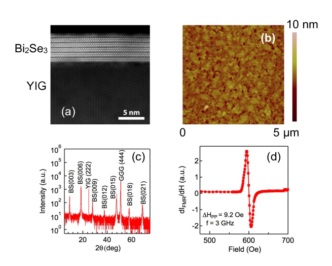
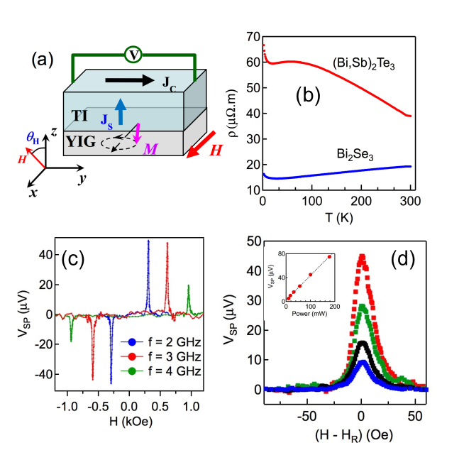
We first discuss the structural and interfacial characterization of the YIG/Bi2Se3 heterostructure using high-resolution scanning transmission electron microscopy (HR-STEM). Figure 1(a) shows an atomically ordered 6 QL Bi2Se3 layer grown on an epitaxial 30-nm YIG thin film. We note that an amorphous layer of about 1 nm in thickness is observed at the YIG/Bi2Se3 interface, most likely due to the nucleation of the template layer in the two-step growth process (see Supplementary Material at [link to be added] for more details about the growth method). The atomic force microscopy (AFM) image in Fig. 1(b) shows a smooth surface with a roughness of about 0.71 nm. A representative x-ray diffraction (XRD) scan of a 40 QL Bi2Se3 film shown in Fig. 1(c) indicates a phase-pure Bi2Se3 layer. Figure 1(d) shows a representative FMR derivative absorption spectrum for a 30-nm YIG film used in this study taken at a radio-frequency (rf) GHz with a magnetic field applied in the film plane. The peak-to-peak line width () obtained from the spectrum is 9.2 Oe, and an effective saturation induction of 1.76 kOe is extracted from fitting the frequency dependence of the resonance field Chang_2014 . The spin pumping measurements are performed using a microwave transmission line on the YIG/TI bilayers at room temperature (approximate sample dimensions of 1 mm 5 mm). During the measurements, a DC magnetic field is applied in the --plane and the spin pumping voltage is measured across the mm long TI layer along the -axis, as illustrated in Fig. 2(a). At the resonance condition, the YIG magnetization precesses around the equilibrium position and transfers angular momentum to the conduction electrons in the TI films through interfacial exchange coupling Du_2013 . The resulting pure spin current is injected along the -axis with spin polarization parallel to , and then converted to a charge current leading to the spin pumping signals.
Figure 2(b) shows the temperature dependence of the resistivity of 6 QL Bi2Se3 and (Bi,Sb)2Te3 thin films grown on YIG. The metallic behavior (decrease in resistivity at low temperature) is the typical behavior of Bi2Se3 due to Se vacancies Kandala_2013 . For (Bi,Sb)2Te3, the resistivity increases by from room temperature to 2 K, consistent with surface state dominated transport in this thin film JSLee_2015 . The carrier concentrations obtained from Hall effect measurements at room temperature are cm-2 and cm-2 for 6 QL Bi2Se3 and (Bi,Sb)2Te3, respectively.
Figure 2(c) shows the observed vs. spectra of the YIG/Bi2Se3 (6QL) bilayers at 2, 3, and 4 GHz using 100 mW microwave power. The observed spin pumping signals change sign when the magnetic field is reversed from to , as expected from either IREE or ISHE. At 2 and 3 GHz, the observed signal is about 40 V, and for 4 GHz, the signal decreases to about 20 V, which results from the variation of the microwave transmission line performance at different frequencies. Figure 2(d) shows the spin pumping spectra of a YIG/Bi2Se3 (6 QL) sample at microwave powers of 18, 32, 56, and 100 mW and an excitation frequency of 3 GHz. The upper inset shows the rf-power dependence of at , indicating that the observed spin pumping signals are in the linear regime.
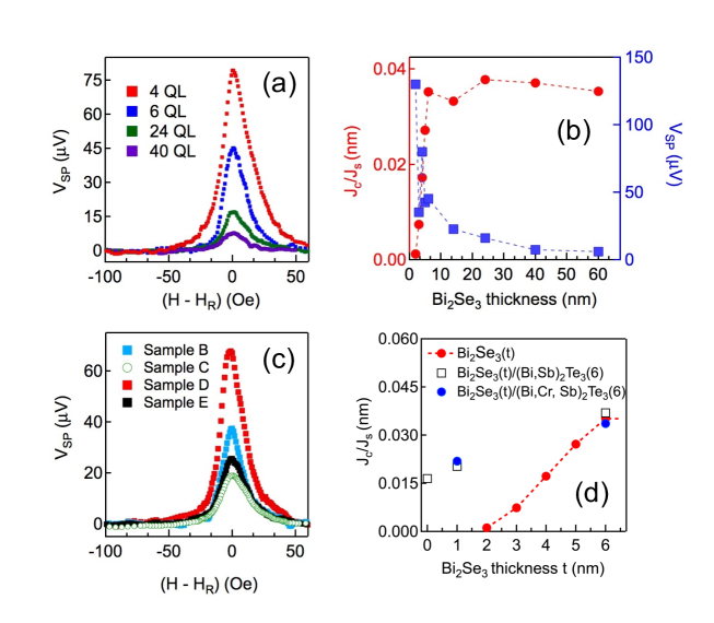
To probe the spin to charge conversion mechanism in TI layers, we systematically vary the Bi2Se3 thickness from 2 to 60 QL. Figure 3(a) shows the spin pumping spectra when for 4, 6, 24, and 40 QL thicknesses of Bi2Se3 grown on YIG, respectively. The significant enhancement of the spin pumping signal in the low Bi2Se3 thickness regime mainly results from the increased resistivity. For a 2D material system, such as the TI surface states, the spin to charge conversion is dominated by IREE [22, 23] and the injected spin current is converted into a 2D charge current, . The spin current density is in units of A m-2, and the 2D charge current density is in units of A m-1; the parameter has the dimension of length and is introduced to characterize the spin to charge conversion efficiency in 2D material systems Sanchez_2013 ; Shen_2014 . The observed spin pumping voltages dominated by IREE depend on several material parameters Sanchez_2013 :
| (1) |
where and are the sample width and resistance, respectively. is the spin current density at the YIG/TI interface which can be expressed as Mosendz_2010 ; Hahn_2013 ; Wang_2014 :
| (2) |
where is the effective interfacial spin mixing conductance Tserkovnyak_2005 , is the FMR peak-to-peak linewidth, is the radio frequency field, is the FMR angular frequency, and is the saturation induction of the YIG thin films. We can determine the effective spin mixing conductance from the FMR linewidth broadening of the YIG thin film Heinrich_2011 ; Mosendz_2010 ; Tserkovnyak_2005 :
| (3) |
where is the absolute gyromagnetic ratio, denotes the thickness of the YIG thin films, is the Landé factor, and is the Bohr magnetron.
If the spin pumping signal is dominated by the ISHE, spin diffusion should be taken into account according to , and the spin pumping signal will follow Heinrich_2011 ; Mosendz_2010 ; Wang_2014 :
| (4) |
where is the spin diffusion length, is the thickness of the TI thin film and is the spin Hall angle. The distinct difference between Eqs. (1) and (4) is whether the observed spin pumping signal is dominated by the spin momentum “locking” in the surface states Liu_2015 ; Tang_2014 ; Li_2014 or by the SOC interaction.
To answer this question, Fig. 3(b) shows the Bi2Se3 thickness dependence of (blue points) and (or ) (red points), where we define . Above 6 QL, almost follows a constant value of about 35 pm. Below 6 QL, dramatically decays by a factor of 30 from pm to pm when at 2 QL thickness. Earlier studies have reported that the thickness of the Bi2Se3 surface states is approximately 2-3 nm YZhang_2010 ; Neupane_2014 . Above 6 QL, the top and bottom Bi2Se3 surface states decouple from each other; below 6 QL, the interaction of the two surface states with opposite spin polarizations can decrease the interfacial spin momentum “locking” efficiency. This is consistent with angle-resolved photoemission spectroscopy (ARPES) studies that show the opening of a gap in the Dirac cone when the Bi2Se3 thickness is below 6 QL, accompanied by a decrease in the spin polarization of the surface states YZhang_2010 ; Neupane_2014 . Qualitatively, our data shown in Fig. 3(b) follow this trend and strongly indicate the key role played by the surfaces states in spin-charge conversion in Bi2Se3. If we try to interpret the data in Fig. 3(b) with the spin diffusion model (Eq. 4), the fit yields a value of nm and also requires the presence of a “dead” layer at the interface (see Supplementary Material at [link to be added] for detailed analysis using the spin diffusion model). This short vertical spin diffusion length suggests that the spin polarized electron current is restricted to the bottom surface of the TI. Thus, while we cannot definitively rule out the spin diffusion model, a more physically meaningful picture at this stage is that the surface states probably play a dominant role in the spin-charge conversion. We note that the value we obtain for (or ) is approximately two orders of magnitude smaller than the spin Hall angle reported using a spin torque FMR study at room temperature Mellnik_2014 . One possible reason for this discrepancy is the amorphous layer at the interface shown in the HR-STEM figure, which potentially decreases the spin injection efficiency. Another reason may be the difference in the fundamental measurement mechanism between these two probing techniques. In a spin torque FMR experiment, as the charge current flows through the TI layers, the electrons can potentially have multiple scattering processes to transfer the spins to the ferromagnetic layers. However, in an FMR spin pumping measurement, this multiple scattering process may not be valid.
To further verify that the spin-charge conversion efficiency is dominated by the surface states of TIs, we grew five different TI heterostructures on YIG as control samples and measured their spin pumping signals. The five control samples are sample A: YIG/(Bi,Sb)2Te3 (6 QL); sample B: YIG/Bi2Se3 (1 QL)/(Bi,Sb)2Te3 (6 QL); sample C: YIG/Bi2Se3 (6 QL)/(Bi,Sb)2Te3 (6 QL); sample D: YIG/Bi2Se3 (1 QL)/Cr0.2(Bi0.5Sb0.5)1.8Te3 (6 QL); and sample E: YIG/Bi2Se3 (6 QL)/Cr0.2(Bi0.5Sb0.5)1.8Te3 (6 QL). Figure 3(c) shows the spin pumping spectra of control samples B, C, D and E at 3 GHz radio-frequency and 100 mW power. The enhancement of the spin pumping signal of samples D and E mainly results from the larger resistivity of Cr0.2(Bi0.5Sb0.5)1.8Te3 compared to (Bi,Sb)2Te3. Normalizing by the resistance and sample width, we obtained the spin charge conversion ratio of the five control samples and compared them with the values for YIG/Bi2Se3 in Fig. 3(d). First, the values of obtained for sample C and sample E are pm and pm, respectively. Both the values are quite close to pm measured for YIG/Bi2Se3 (6QL), indicating that as long as the Bi2Se3 thickness is above 6 QL, the spin-charge conversion efficiency is roughly constant and does not depend on the bulk properties: Cr doping and different band structures do not change the values. Second, for sample A, (Bi,Sb)2Te3 directly grown on YIG, pm, about half of the value of Bi2Se3. This is in sharp contrast with earlier results which reported a much larger spin Hall angle of the (Bi,Sb)2Te3 compared with Bi2Se3 using a spin-polarized tunneling study Shen_2014 . This most likely results from the different interfacial quality and conditions that determine the spin momentum “locking” efficiency. We expect that the bottom surface state condition at the YIG/(Bi,Sb)2Te3 interface YZhang_2010 is not as good as the CoFeB/MgO/(Bi,Sb)2Te3 interface Shen_2014 for which TI was grown on the commercial InP substrates with minimal lattice mismatch and the highest sample quality. In the end, we compare the values in samples B and D that both have 1 QL Bi2Se3 seed layers. For sample D, we intentionally dope the (Bi,Sb)2Te3 with Cr, which can induce ferromagnetism at low temperature Jiang_2015 . At room temperature, the Cr doping mainly changes the transport properties and the SOC strength of the bulk states. The values for samples B and D are pm and pm, respectively. Their similar spin-charge conversion efficiencies demonstrate that the properties of the TI bulk state do not play a significant role here, confirming the interface-dominated spin pumping phenomena. It is also important to note that values of for samples B and D are lower than the value for YIG/Bi2Se3 (6QL). As in other studies of spin pumping into TIs, the interfacial condition presents a critical challenge for controlling the spin conversion efficiency Shiomi_2014 ; Deorani_2014 ; Jamali_2015 ; in sample B, both YIG/Bi2Se3 and Bi2Se3 /(Bi,Sb)2Te3 interfaces will contribute to the formation of the surface states. Thus, structural defects and/or strain induced dislocations in the trilayer heterostructures can potentially result in the observed lower values. A thorough understanding about the correlation of the interfacial conditions of TI surfaces states and the spin-charge conversion efficiency requires further investigation.
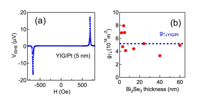
Finally, we compare the spin transfer efficiency at YIG/Bi2Se3 to that at YIG/Pt. Note that Pt is an ideal spin sink and a well-studied non-magnetic material with large SOC Mosendz_2010 ; Wang_2014 . Figure 4(a) shows the inverse spin Hall spectrum of a YIG(30nm)/Pt(5nm) bilayer sample under 3 GHz and 100 mW microwave power when the field is in plane. The observed sign change of the spin pumping signal with field reversal is expected for the ISHE in a 3D material system Heinrich_2011 ; Mosendz_2010 . From the FMR linewidth broadening, the obtained YIG/Pt effective spin mixing conductance is , which lies in the range of the values reported by other groups using spin pumping Hahn_2013 ; Wang_2014 . We compare this value with the obtained spin mixing conductance at various Bi2Se3 thicknesses in Fig. 4(b). When Bi2Se3 is 6 QL thick, the spin mixing conductance at the YIG/Bi2Se3 interface is . Although there are some variations, the reported values are in the range of when the Bi2Se3 thickness varies from 2 to 60 QL, which is essentially comparable to the determined value at the YIG/Pt interface, demonstrating an efficient spin transfer in YIG/TI heterostructures. It is important to note that in the large Bi2Se3 thickness regime, we do not observe an enhancement of , which is typically observed in the YIG/transition metal bilayers due to the decrease in backflow spin current caused by the spin diffusion in the bulk Tserkovnyak_2005 ; Jiao_2013 . This also confirms the TI surface states dominated spin-charge conversion mechanism.
In conclusion, we report robust spin pumping at room temperature in YIG/Bi2Se3 bilayers and other YIG/TI heterostructures. By measuring IREE voltages and interfacial spin current density, we determine the value of and reveal its systematic behavior with Bi2Se3 thickness, demonstrating the dominant role of surface states in spin-charge conversion. The inferred IREE length indicates the important role of interface conditions in spin Hall physics in topological insulators. Further investigation is required for a thorough understanding of the correlation between the formation of the surface states and the variation of spin-charge conversion efficiency at the interfaces.
Acknowledgements.
The work at Penn State, Colorado State and University of Minnesota is supported by the Center for Spintronic Materials, Interfaces, and Novel Architectures (C-SPIN), a funded center of STARnet, a Semiconductor Research Corporation (SRC) program sponsored by MARCO and DARPA. NS and AR acknowledge additional support from ONR- N00014-15-1-2364. TL, HC, and MW acknowledge additional support from NSF-ECCS-1231598 and ARO-W911NF-14-1-0501. This work utilized (1) the College of Science and Engineering (CSE) Characterization Facility, University of Minnesota (UM), supported in part by NSF through the UMN MRSEC program (No. DMR-1420013); and (2) the CSE Minnesota Nano Center, UM, supported in part by NSF through the NNIN program.References
- (1) Y. Kajiwara, K. Harii, S. Takahashi, J. Ohe, K. Uchida, M. Mizuguchi, H. Umezawa, H. Kawai, K. Ando, K. Takanashi, S. Maekawa, and E. Saitoh, Nature 464, 262 (2010).
- (2) B. Heinrich, C. Burrowes, E. Montoya, B. Kardasz, E. Girt, Y.-Y. Song, Y. Y. Sun, and M. Z. Wu, Phys. Rev. Lett. 107, 066604 (2011).
- (3) O. Mosendz, V. Vlaminck, J. E. Pearson, F. Y. Fradin, G. E. W. Bauer, S. D. Bader, and A. Hoffmann, Phys. Rev. B 82, 214403 (2010).
- (4) C. H. Du, H. L. Wang, Y. Pu, T. L. Meyer, P. M. Woodward, F. Y. Yang, and P. C. Hammel, Phys. Rev. Lett. 111, 247202 (2013).
- (5) C. Hahn, G. de Loubens, O. Klein, M. Viret, V. V. Naletov, and J. Ben Youssef, Phys. Rev. B 87, 174417 (2013).
- (6) H. L. Wang, C. H. Du, Y. Pu, R. Adur, P. C. Hammel, and F. Y. Yang, Phys. Rev. Lett. 112, 197201 (2014).
- (7) J.-C. Rojas-S nchez, L. Vila, G. Desfonds, S. Gambarelli, J. P. Attan , J. M. De Teresa, C. Mag n, and A. Fert, Nat. Commun. 4, 2944 (2013).
- (8) Y. Shiomi, K. Nomura, Y. Kajiwara, K. Eto, M. Novak, K. Segawa, Y. Ando, and E. Saitoh, Phys. Rev. Lett. 113, 196601 (2014).
- (9) A. R. Mellnik, J. S. Lee, A. Richardella, J. L. Grab, P. J. Mintun, M. H. Fischer, A. Vaezi, A. Manchon, E.-A. Kim, N. Samarth, and D. C. Ralph, Nature 511, 449 (2014).
- (10) Y. Fan, P. Upadhyaya, X. Kou, M. Lang, S. Takei, Z. Wang, J. Tang, L. He, L.-T. Chang, M. Montazeri, G. Yu, W. Jiang, T. Nie, R. N. Schwartz, Y. Tserkovnyak, and K. L. Wang, Nat. Mater. 13, 699 (2014).
- (11) P. Deorani, J. Son, K. Banerjee, N. Koirala, M. Brahlek, S. Oh, and H. Yang, Phys. Rev. B 90, 094403 (2014).
- (12) M. Jamali, J. S. Lee, J. S. Jeong, F. Mahfouzi, Y. Lv, Z. Zhao, B. K. Nikolic, K. A. Mkhoyan, N. Samarth, and J.-P. Wang, Nano Lett. 15, 7126 (2015).
- (13) A. A. Baker, A. I. Figueroa, L. J. Collins-McIntyre, G. van der Laan, and T. Hesjeda, Scientific Reports 5, 7907 (2015).
- (14) Y. Wang, P. Deorani, K. Banerjee, N. Koirala, M. Brahlek, S. Oh, and H. Yang, Phys. Rev. Lett. 114, 257202 (2015).
- (15) K. Kondou, R. Yoshimi, A. Tsukazaki, Y. Fukuma, J. Matsuno, K. S. Takahashi, M. Kawasaki, Y. Tokura, and Y. Otani, arXiv:1510.03572.
- (16) D. Hsieh et al., Nature 460, 1101 (2009).
- (17) M. Z. Hasan and C. L. Kane, Rev. Mod. Phys. 82, 3045 (2010).
- (18) X. -L. Qi and S. -C. Zhang, Rev. Mod. Phys. 83, 1057 (2011).
- (19) H. Chang, P. Li, W. Zhang, T. Liu, A. Hoffmann, L. Deng, and M. Z. Wu, IEEE Magn. Lett. 5, 6700104 (2014).
- (20) A. Kandala, A. Richardella, D. W. Rench, D. M. Zhang, T. C. Flanagan, and N. Samarth, Appl. Phys. Lett. 103, 202409 (2013).
- (21) J. S. Lee, A. Richardella, D. Reifsnyder Hickey, K. A. Mkhoyan, and N. Samarth, Phys. Rev. B 92, 155312 (2015).
- (22) V. M. Edelstein, Solid State Commun. 73, 225 (1990).
- (23) K. Shen, G. Vignale, and R. Raimondi, Phys. Rev. Lett. 112, 096601(2014).
- (24) Y. Tserkovnyak, A. Brataas, G. E.W. Bauer, and B. I. Halperin, Rev. Mod. Phys. 77, 1375 (2005).
- (25) L. Liu, A. Richardella, I. Garate, Y. Zhu, N. Samarth, and C.-T. Chen, Phys. Rev. B 91, 235437 (2015).
- (26) J. Tang, L.-T. Chang, X. Kou, K. Murata, E. S. Choi, M. Lang, Y. Fan, Y. Jiang, M. Montazeri, W. Jiang, Y. Wang, L. He, and K. L. Wang, Nano Lett. 14, 5423 (2014).
- (27) C. H. Li, O. M. J. van’t Erve, J. T. Robinson, Y. Liu, L. Li, and B. T. Jonker, Nat. Nanotechnol. 9, 218 (2014).
- (28) Y. Zhang et al., Nat. Phys. 6, 584 (2010).
- (29) M. Neupane et al., Nat. Commun. 5, 3841 (2014).
- (30) Z. Jiang, C.-Z. Chang, C. Tang, P. Wei, J. S. Moodera, and J. Shi, Nano Lett. 15, 5835 (2015).
- (31) A. Kandala, A. Richardella, S. Kempinger, C.-X. Liu, and N. Samarth, Nat. Commun. 6, 7434 (2015).
- (32) H. J. Jiao and G. E. W. Bauer, Phys. Rev. Lett. 110, 217602 (2013).