TARGET 5: a new multi-channel digitizer with triggering capabilities for gamma-ray atmospheric Cherenkov telescopes
Abstract
TARGET 5 is a new application-specific integrated circuit (ASIC) of the TARGET family, designed for the readout of signals from photosensors in the cameras of imaging atmospheric Cherenkov telescopes (IACTs) for ground-based gamma-ray astronomy. TARGET 5 combines sampling and digitization on 16 signal channels with the formation of trigger signals based on the analog sum of groups of four channels. We describe the ASIC architecture and performance. TARGET 5 improves over the performance of the first-generation TARGET ASIC, achieving: tunable sampling frequency from GSa/s to GSa/s; a dynamic range on the data path of 1.2 V with effective dynamic range of 11 bits and DC noise of mV; 3-dB bandwidth of 500 MHz; crosstalk between adjacent channels ; charge resolution improving from 40% to between 3 photoelectrons (p.e.) and p.e. (assuming 4 mV per p.e.); and minimum stable trigger threshold of 20 mV (5 p.e.) with trigger noise of 5 mV (1.2 p.e.), which is mostly limited by interference between trigger and sampling operations. TARGET 5 is the first ASIC of the TARGET family used in an IACT prototype, providing one development path for readout electronics in the forthcoming Cherenkov Telescope Array (CTA).
keywords:
gamma rays , imaging atmospheric Cherenkov telescope , application-specific integrated circuit , waveform sampling , trigger , digitizer , Cherenkov Telescope ArrayPACS:
07.50.Qx , 95.55.Ka1 Introduction
In the past three decades, imaging atmospheric Cherenkov telescopes (IACTs) have greatly advanced observations of very-high-energy gamma-ray emission from the Universe, with numerous implications for astrophysics, particle physics, and cosmology [e.g., 1]. This field is soon going to be revolutionized with the advent of the Cherenkov Telescope Array (CTA) [2], which is going to increase the source sensitivity by an order of magnitude at energies from 100 GeV to 10 TeV and to extend observations to the ranges well below 100 GeV and above 100 TeV.
The performance requirements of CTA drive innovation to improve performance and lower cost. One innovative design is the Schwarzschild–Couder telescope [3], which features dual-mirror optics for excellent optical performance (focusing of Cherenkov photons) and a reduced camera plate scale compared to the traditional single-mirror (Davies-Cotton) design used so far for IACTs. The reduced camera size enables compact, inexpensive, densely pixelated photodetectors such as silicon photomultipliers. The optical performance combined with dense pixellation provides improved field of view, angular resolution, and hadronic background rejection capabilities [4].
TARGET is an application-specific integrated circuit (ASIC) series that has been designed for the processing of the photodetector signals in such telescopes. The goals in the inception of TARGET were to keep the costs low and integrate several functionalities in a compact design. We have described the concept of TARGET 1, the first generation of ASICs of the TARGET family, and characterized its performance in [5]. Several improvements drove the development of TARGET 5 (after a few design iterations), which is described in this paper.
TARGET 5 is the first chip of the TARGET family to be used in a telescope prototype, namely a prototype of the Gamma-ray Cherenkov Telescope (GCT) [6], a Schwarzschild–Couder small-sized telescope proposed in the framework of the CTA project. TARGET 5 is used in the first prototype of the GCT camera, also known as Compact High Energy Camera with MAPMTs (CHEC-M) [7, 8]. TARGET is also planned to be used in a medium-sized telescope proposed in the framework of the CTA project, namely the Schwarzschild-Couder Telescope (SCT) [9].
Key features of TARGET are:
-
1.
a compact design that combines signal sampling and digitization, as well as triggering, for 16 channels in a single chip, which lowers the cost111 per channel for the realization discussed in this paper, estimated $20 per channel in a large production on the scale required for several dozen CTA telescopes., improves on reliability further reducing maintenance costs, and enables the use with compact photodetectors such as multi-anode photomultiplier tubes (MAPMTs) or silicon photomultipliers in a compact camera design
-
2.
a sampling frequency tunable up to GSa/s, ideally suited for the measurement of the ns pulses from Cherenkov flashes
-
3.
a deep buffer (16,384 samples in TARGET 5) for large trigger latency tolerance between distant ( km) telescopes222Within CTA, using a hardware coincidence trigger between telescopes is not planned for GCTs, but it is foreseen for SCTs.
-
4.
dynamic range bits
-
5.
moderate power consumption, for the applications described in this paper mW per channel
TARGET ASICs are implemented for IACTs into front-end electronics modules that combine all the functions described above to read out 64 photodetector pixels using six or fewer printed circuit boards, four ASICs, and a companion field-programmable gate array (FPGA) [5]. The low number of components supports affordability and reliability.
The structure of this paper is as follows. Section 2 describes the architecture of the TARGET 5 ASIC. Section 3 presents the characterization of its performance, including sampling and digitization in 3.2, as well as triggering in 3.3. Section 4 briefly outlines how TARGET 5 is implemented into front-end electronics modules for CHEC-M, and Section 5 presents the conclusions and outlook.
2 The TARGET 5 architecture
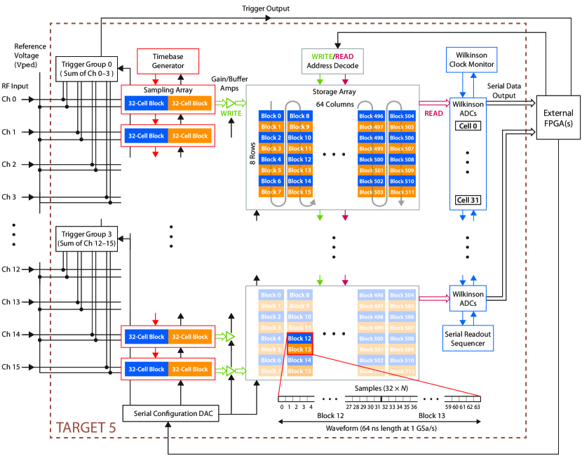
Fig. 1 presents an overview of the major functional blocks of the TARGET 5 ASIC: triggering, analog sampling and storage, analog-to-digital converters (ADC), and configuration of control features and digital-to-analog converters (DAC) provided via a serial-parallel interface.
The general features of TARGET 5 detailed in the following text are summarized in Table 1 with comparison to TARGET 1.
| TARGET 1 | TARGET 5 | |
| Number of channels | 16 | 16 |
| Dynamic range of digitizer (bits) | 9 or 10 | 12 |
| Sampling frequency (GSa/s) | to | to |
| 3-dB analog bandwidth (MHz) | 150 | 500 |
| Crosstalk at 3 dB frequency | ||
| Size of storage array (cells per channel) | 4,096 | 16,384 |
| Wilkinson ADC counter speed (MHz) | 445 | |
| Minimum digitization block (number of cells) | 16 | 32 |
| Digitization time per block (s) | 2.3 (10 bit) | 5.9 (12 bit) |
| Number of Wilkinson ADCs | 32 | 512 |
| Number of cells digitized simultaneously | channels | channels |
| Clock speed for serial data transfer (Mbps) | – | 109 |
| Channels for simultaneous data transfer | – | 16 |
| Trigger outputs | 1 (OR of 16 channels) | 4 (analog sum of 4 channels) |
As with TARGET 1 and other predecessors in the TARGET family, TARGET 5 is a 16-channel device where both a signal and its reference signal (an input pedestal voltage, Vped) are input to the ASIC, to provide a modest amount of common-mode noise rejection, as well as reference for the trigger gain path. The input signal is simultaneously processed for sampling (data path) and triggering (trigger path).
ASICs of the TARGET family use switched capacitor arrays (SCAs) to sample signals at very high sampling rate, i.e., the input is connected to an array of capacitors via analog switches which are sequentially connected and disconnected to sample the signal at regular intervals.
The sampling buffer depth (16 s) needed to trigger using coincidence between distant (up to 1 km) telescopes requires several thousand storage capacitors given a sampling frequency of 1 GSa/s. Directly driving the capacitance of such an array limits its analog bandwidth. Therefore, one of the major improvements of TARGET 5 over TARGET 1 is the separation of sampling operations into two stages in order to simultaneously achieve large bandwidth and a deep buffer for trigger decisions. In the first stage, an SCA with a small number of cells (two blocks of 32 cells), called the sampling array, is used for signal sampling in order to reduce the capacitance load on the input. In the second stage, the samples are transferred to an SCA with a large number of cells (16,348), called the storage array, which provides the desired buffer depth. While acquisition occurs in one group of 32 cells in the sampling array, the other is written to the storage array. This ping-pong approach provides continuous sampling.
Control of the sample timing is provided by a timebase generator that is driven by two digital signals sent from the FPGA to the ASIC: SSTin and SSPin. These signals go through time delay elements that are current-starved inverters and control charge tracking and hold in the SCAs. The sampling speed of TARGET 5 is controlled by adjusting the supply current for the inverter in the delay elements.
Previous measurements of our timebase generator indicated that the sampling speed is temperature dependent with a coefficient of approximately 0.2% per [10]. In order to reuce this effect, there are two mechanisms available in TARGET 5. The ASIC is equipped with a continuous ring oscillator copy of the timebase generator (with one additional inverter) and its output is available for external monitoring and feedback control in firmware/software. The delayed copy of SSTin after the full chain of time delay elements, SSTout, is also available for monitoring and feedback.
Blocks of 32 storage cells are randomly accessible for readout from the storage array on demand. Once selected, the 32 storage cells in all 16 channels are powered up for Wilkinson ADCs. A Wilkinson ramp voltage generator block generates and broadcasts a ramp with adjustable duration and slew rate to all channels. The Wilkinson ramp slew rate is adjusted by varying the capacitor charging current, denoted Isel, or by changing an external ramping capacitor.
At a separately controllable start time, a 12-bit ripple counter (with adjustable speed) is begun for each channel. In order to support the fastest possible digitization, separate oscillators are provided for each counter. When the voltage ramp crosses the comparator threshold for a given sample voltage, the counter stops and the count then represents the time (ADC code) corresponding to the voltage held in the storage cell. In order to maintain a constant Wilkinson clock rate as a function of temperature, a separate, identical Wilkinson counter is provided inside the Wilkinson clock block for monitoring and feedback. Address decoding and sequencing is performed inside a serial readout sequencer block. Digitized values are randomly accessible for serial transfer on all 16 channels in parallel.
Digitization and readout can occur on demand, initiated by an external trigger signal. This external trigger signal can be generated by external logic based on the trigger primitives generated by TARGET 5 itself. Trigger primitives are formed based on the analog sum of four adjacent channels, referred to as a trigger group. Each ASIC provides four trigger primitives from four independent trigger groups. To compensate for channel-to-channel photodetector gain variations, bias voltages are provided to tune the gain of each channel (before the analog sum) between 1 and 6.5. Furthermore, the contribution from each individual channel to the sum can be disabled in order to mask out noisy channels. The summed signal is routed to a comparator for thresholding.
3 Performance
3.1 Evaluation board and software
Evaluation of TARGET 5 performance has been carried out using the dedicated board shown in Figure 2. It features a TARGET 5 ASIC and an FPGA (Xilinx Virtex-5) as well as all the ancillary components necessary to support them. The FPGA controls the ASIC and connects to an external computer through a fiber interface. External termination resistors are used in order to set the real part of the input impedance to 50 for interfacing with standard cables (the same strategy is adopted for the front-end electronics camera module described in Section 4).
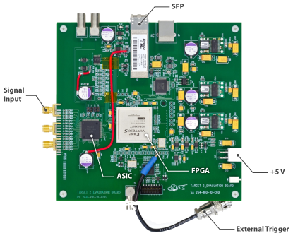
The external computer and the evaluation board FPGA communicate with each other through an optical fiber/Gigabit ethernet cable via the User Datagram Protocol (UDP). The control and data acquisition software, libTARGET, is written in C++11 to support both POSIX and Windows systems, and supports the generation of a Python wrapper. The latest version of libTARGET can be obtained from the authors upon request.
3.2 Data path
3.2.1 Sampling
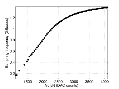
The analog sampling frequency is determined by two control voltages, VdlyP and VdlyN, which set the supply and sink current for the time delay elements, respectively. Each control voltage is supplied by a digital-to-analog converter (DAC) internal to the ASIC controlled through the serial-parallel interface.
The measured sampling frequency as a function of VdlyN is shown in Figure 3. This measurement was made at room temperature, with VdlyP set to 1616 DAC counts. The sampling frequency was measured by recording a sinusoid of known frequency from a function generator and fitting to determine the sampling frequency. In general, frequencies from 0.2 to 1.4 GSa/s are possible. However, the FPGA firmware must support a particular frequency in order to use it. To maintain phase alignment while wrapping around the primary sampling buffer of 64 samples, 64 samples must be a multiple of 8 ns (one tick of the 125 MHz FPGA clock). This limits the available frequencies to a discrete set: 1.33 GSa/s, 1.14 GSa/s, 1.00 GSa/s, etc. The frequencies that were explicitly supported in the FPGA firmware and tested are 1 GSa/s and 0.4 GSa/s. Measurements presented in this paper were performed with a sampling frequency of 1 GSa/s.
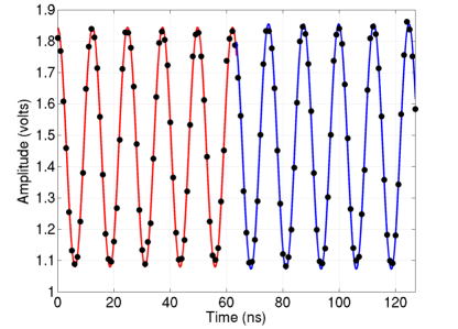
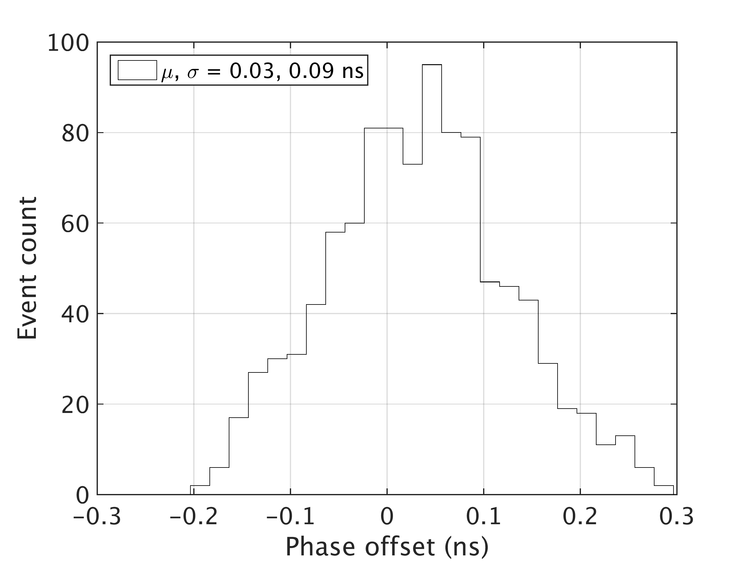
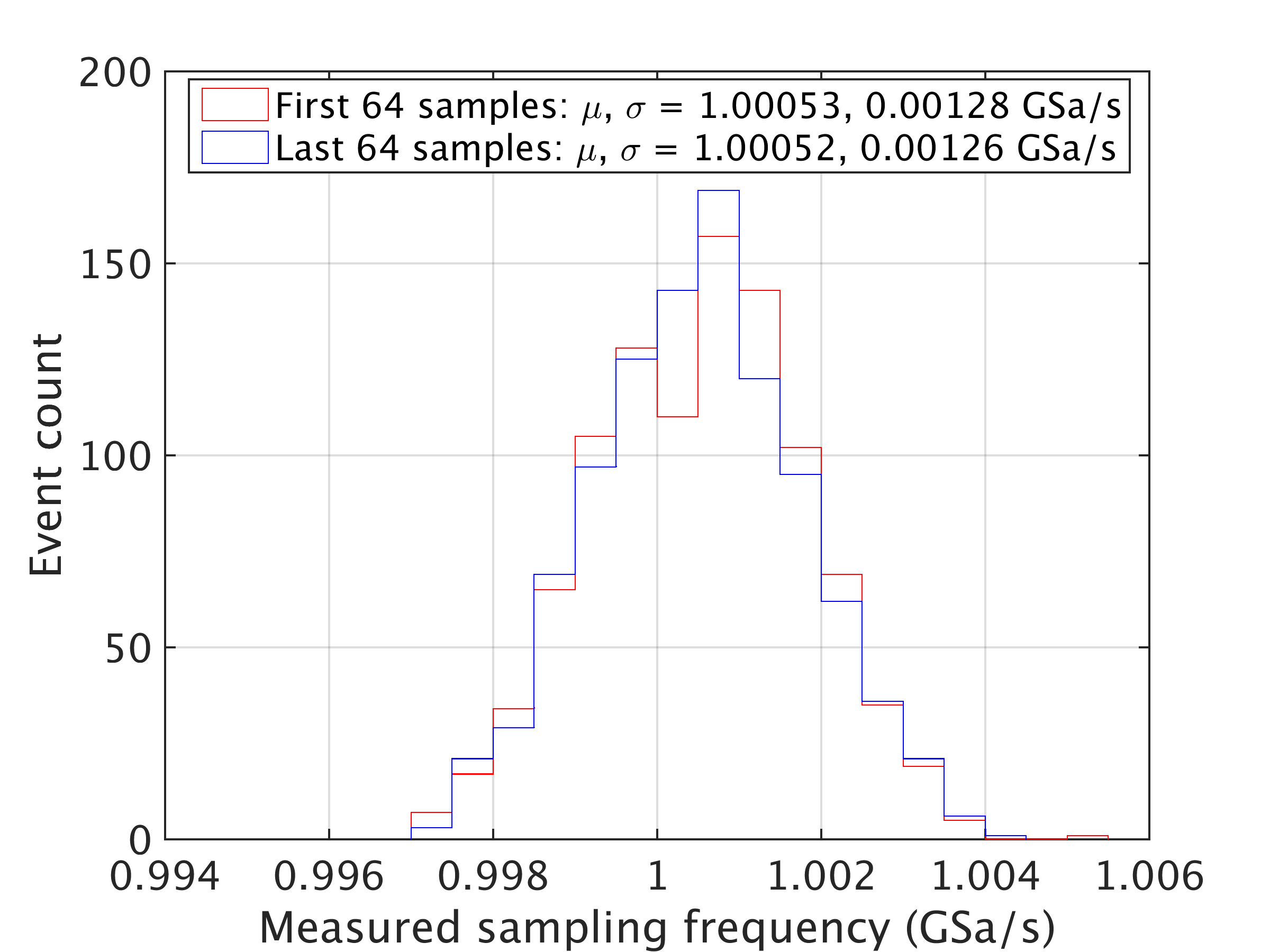
Precise timing is necessary to maintain a constant sampling frequency, particularly when wrapping around the primary sampling buffer. For fixed VdlyN, the sampling frequency varies with temperature. A feedback algorithm is used to control VdlyN in order to achieve a stable sampling frequency despite temperature variation. Several feedback mechanisms (implemented on the companion FPGA) were evaluated using a thermal chamber to vary the temperature between ∘C and ∘C. An example waveform illustrating the achieved sampling frequency precision, as well as histograms of the wrap-around timing alignment and measured sampling frequency, are shown in Figure 4. In this case a digital clock manager in the FPGA is used for feedback. The phase of SSTout (delayed copy of one of the input timing signals, SSTin, after all the time delay elements) is stabilized against drift due to temperature variation and other causes by the feedback loop controlling VdlyN. Feedback loop parameters were optimized based on measurements of sinusoids in the thermal chamber. This feedback loop achieves good temperature stability, corresponding to a phase gap of 0.1 ns introduced between succeeding blocks by a temperature change of 10∘ C. Alternative feedback algorithms achieve slightly smaller temperature dependence and slightly larger event-to-event variation in sampling frequency.
3.2.2 DC transfer function and noise
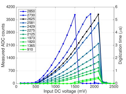
The DC transfer function (measured ADC counts as a function of input signal amplitude) depends on several configuration parameters. The most important is Isel, which controls the ramp capacitor charging current333Specifically, Isel controls the bias voltage for the current mirror that generates the charging current. Larger Isel values correspond to smaller currents., hence the slew rate of the Wilkinson ramp. Isel is set by an internal DAC. The dependence of the transfer function and of the digitization time on Isel is shown in Figure 5. For a given Wilkinson clock frequency and DC signal amplitude, increasing Isel slows the ramp, increasing the digitization time but also improving the voltage resolution. For a given application, Isel can be selected to match the required input range and also to choose the tradeoff between digitization time, resolution, and noise.
The Wilkinson counter frequency is selected by the Vdly control voltage. This circuitry has some temperature dependence, resulting in temperature dependence of the transfer function slope. However, the Wilkinson clock frequency can be monitored and used for a control loop that varies Vdly (provided by an internal DAC) in order to stabilize the Wilkinson frequency despite varying temperature. The transfer function was measured at various temperatures in a thermal chamber, both with and without this feedback loop enabled. The results are shown in Figure 6. After enabling feedback, there is a small amount of residual temperature dependence, likely due to temperature sensitivity of other parts of the digitization circuit.
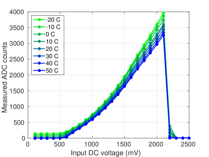
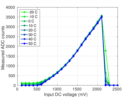
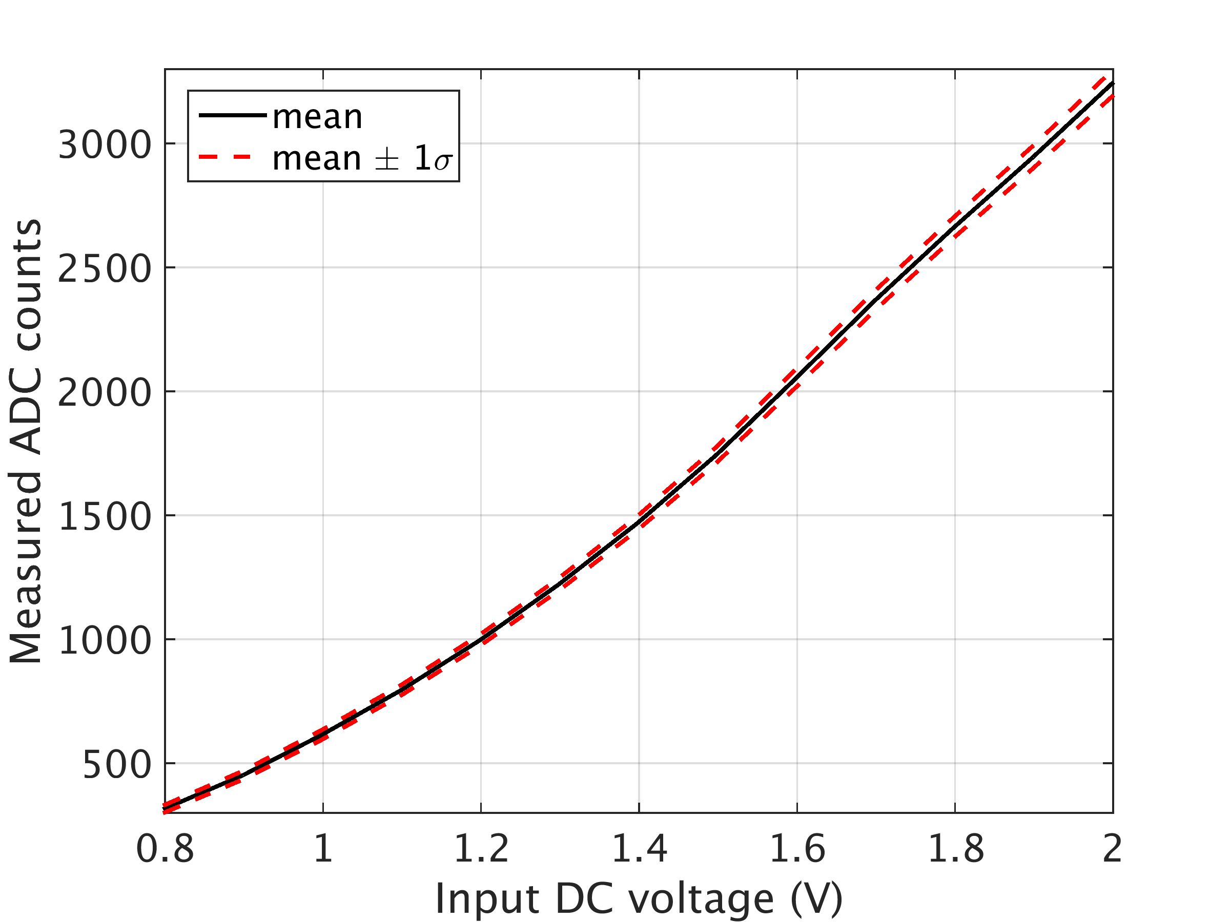
Figure 7 shows an example TARGET 5 transfer function at room temperature for a typical configuration. In general the transfer function depends on both the configuration and on the channel and cell position in the SCA. The integral nonlinearity of the transfer function shown in Figure 7 (with respect to the best linear fit, which has a slope of 2.5 counts/mV) is 212 ADC counts. A calibration procedure is used to remove effects of this nonlinearity from data. Polynomial parameterization of the transfer function (up through fourth order) was evaluated and found to provide insufficient precision. A lookup table was found to be a more precise solution and is implemented in offline analysis software. We found that 25 data points (spanning 0.1 to 2.5 V) are sufficient to specify its shape to a precision better than the DC noise. Variation from cell to cell is included in the calibration procedure but is small, as indicated by the 1 curves in Figure 7.
The transfer function shown in Figure 7 is the result of optimizing for effective dynamic range. The input range is 1.2 V (spanning 0.8 to 2.0 V). This input range spans 315 to 3243 ADC counts, corresponding to 2928 counts (11.5 bits) of resolution. The DC noise, after calibration of the transfer function, was measured (averaged over input DC voltage from 0.8 to 2.0 V) to be 0.6 mV (1.4 ADC counts, or 0.5 least-significant bits). The effective dynamic range is therefore , or, equivalently, bits. This compares favorably with TARGET 1, which has an effective dynamic range of 9.1 bits [5].
3.2.3 ASIC response to sinusoids
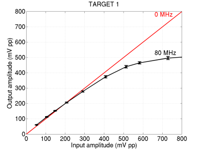
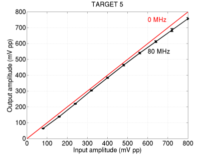
The DC transfer functions described previously are used to convert measured ADC counts to instantaneous input voltage. The ASIC response was also evaluated using sinusoidal signals from a function generator calibrated with the transfer functions determined from DC input. By scanning the input AC amplitude and comparing to the measured amplitude, the TARGET “AC transfer function” is determined (Figure 8). In TARGET 1, high frequency signals were found to exhibit an “AC saturation” effect at large amplitude [5]. Note that this is not an effect due to finite bandwidth, which would cause the AC transfer function to have a slope less than unity but independent of input amplitude. This effect was understood using simulations of TARGET 1 as due to an insufficient slew rate of the input buffer amplifiers and fixed in the design of subsequent revisions. As shown in Figure 8, AC saturation in TARGET 5 is negligible.
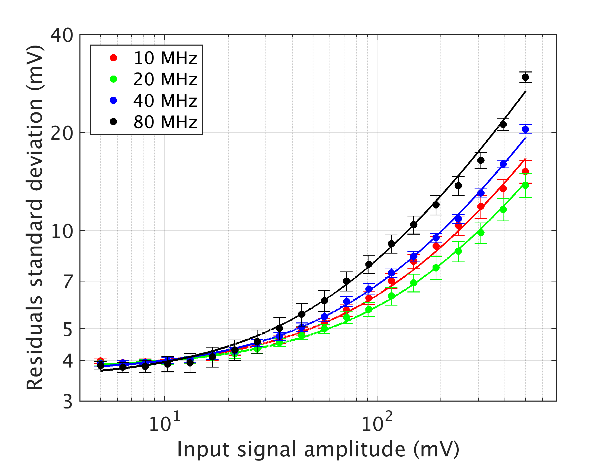
The effective noise measured with sinusoidal signals, i.e., the deviation of waveform samples from the fitted sinusoid, is larger than the noise measured with DC signals, as shown in Figure 9. This effective noise is caused by slightly suboptimal timing performance of the sampling, with a potential additional contribution due to settling of the signals from the sampling to the storage array and hysteresis in the sampling array. Therefore, it is not additive noise independent of the signal but it depends on the signal frequency and amplitude.
For fixed signal frequency, this noise increases linearly with the signal amplitude, as shown in Figure 9. The noise is 80% at 5 mV signal amplitude and decreases to 5% at 500 mV. The relationship between signal and noise is modeled well by a linear fit at each frequency, as indicated by the best-fit curves in Figure 9. The linear dependence supports the hypothesis that the main source of this noise is slightly suboptimal timing performance. The effective noise measured in this configuration with small signal amplitude is 4 mV, independent of signal frequency. This is larger than the 0.6 mV noise measured with DC signals and is most likely due to noise injected by the function generator.444This was confirmed with tests using a different model function generator.
The effective AC noise performance is acceptable for measurements of integrated charge from photodetectors, an application for which photon counting is dominated by Poisson noise at the low amplitude range (limiting resolution to %) and resolution of 10% is typically sufficient for many-photoelectron signals.
3.2.4 Bandwidth
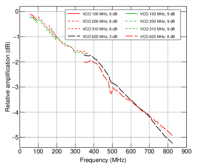
The bandwidth of the TARGET 5 ASIC was measured by comparing the amplitude of input sinusoids to the amplitude of waveforms recorded by the ASIC. To generate a range of sinusoidal input from MHz to MHz, we used four voltage-controlled oscillators (VCOs) whose variable frequencies and amplitudes were calibrated with a fast digital oscilloscope (Tektronix MDO4104-6, GHz 3-dB bandwidth). The amplitudes of recorded waveforms were estimated by calculating the standard deviation of thousands of voltage samples.
Figure 10 shows the measured attenuation of TARGET 5 as a function of input frequency. In this measurement, three different attenuators (, , and dB) were used to repeat the same measurement with different input amplitudes, showing that different combinations of attenuators and VCOs are consistent with one another within dB. The 3-dB bandwidth of TARGET 5 is approximately 500 MHz.
3.2.5 Crosstalk
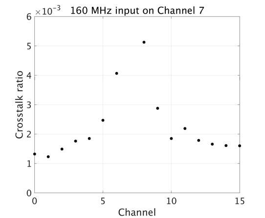
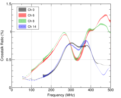
Due to the layout of the ASIC, AC signals induce a small amount of crosstalk on nearby channels. The measurements described in Sections 3.2.3 and 3.2.4 provide two complementary estimates of the crosstalk. In both cases, continuous wave sinusoids of various frequencies were injected to individual channels and we read out all channels. When using the function generator (3.2.3) to estimate the crosstalk we used a large input amplitude (0.8 V peak to peak), and we performed sinusoid fits to all channels, fixing the frequency to the known value. In the case of the VCOs (3.2.4), which extend the measurement to higher frequencies (hence, smaller measured amplitudes), the crosstalk was estimated from the standard deviation of thousands of voltage samples.
Figure 11 shows a summary of the results from the two crosstalk estimates. The two measurements show good quantitative agreement in the frequency range where they overlap between 30 and 160 MHz, where the crosstalk ratio is at most 0.5%. The crosstalk was measured to be largest on nearest neighbors, followed by next-to-nearest neighbors as expected from the layout of the ASIC. The crosstalk ratio shows a marked frequency dependency and below 500 MHz (3dB bandwidth of the ASIC and Nyquist frequency for typical 1 GSa/sec operation) it is at most 1.3%.
3.2.6 ASIC response to pulses
In addition to quantifying the performance of TARGET 5 with sinusoidal signals, we studied the performance with short electrical pulses (from a function generator) similar to those produced by a photodetector after shaping through a preamplifier as planned in CHEC-M [7, 8] and the SCT [9]. This is especially useful for quantifying the impact of the effective noise in terms of photoelectron charge resolution. Each pulse had an 8 ns full width at half maximum, 5 ns rise time, and 5 ns fall time. The amplitude was varied to emulate variation in the number of photoelectrons (p.e.).
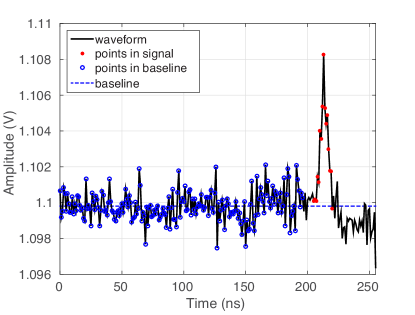
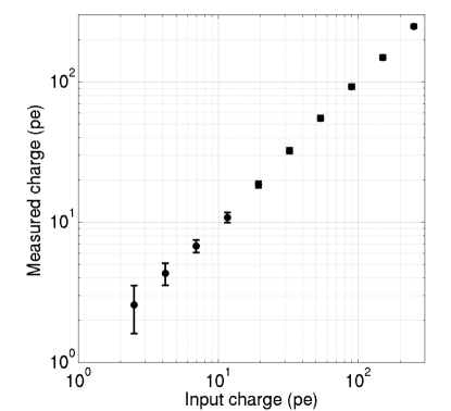
A charge reconstruction algorithm was applied as follows to digitized waveforms recorded using a sampling frequency of 1 Gsa/s. The 17 samples centered on the peak sample are determined and designated as on-pulse. Eight samples before these on-pulse samples are avoided because they lie in the transition region between on-pulse and off-pulse. Furthermore, all samples after the on-pulse samples are avoided because they could include undershoot. The remainder of the samples, well before the pulse, are designated off-pulse. An example waveform with this algorithm applied is shown in Figure 12. The mean of the off-pulse samples is calculated and used as a baseline estimate. The mean of the on-pulse samples is then determined and the baseline is subtracted. The resulting quantity provides an estimate of the baseline-subtracted charge integral in the pulse and increases linearly with the pulse input amplitude. This quantity is calibrated to photoelectrons assuming a preamplifier gain of 4 mV per photoelectron. The resulting measured charge as a function of simulated input charge is shown in Figure 13.
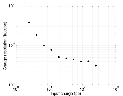
The charge resolution is quantified for each input pulse amplitude by the standard deviation of the reconstructed charge. The relative charge resolution is shown in Figure 14. This charge resolution is dominated by the effective AC noise described in Section 3.2.3. In particular, the increase of effective noise at large amplitudes (Figure 9) causes the charge resolution to plateau for large charge values. In a full system consisting of photodetector plus readout electronics, the charge resolution will be worse than this due to other contributions including photodetector noise, crosstalk, after-pulses, gain uncertainty, and Poisson noise.
3.3 Trigger path
3.3.1 Tuning of the trigger performance
The trigger performance is determined in each trigger group mainly by two parameters, PMTref4, which sets the reference voltage for the summing amplifier that performs the analog sum of the signal from four adjacent channels, and Thresh, which sets the reference voltage for the comparator. Both parameters set the voltages with respect to the corresponding supply voltages (also tunable) and are controlled by a 12-bit DAC.
To characterize the trigger performance, we performed a scan over these parameters. For each setting we injected in one channel pulses of variable amplitude with frequency of 1 kHz, full width at half maximum of 8 ns, and rise time of 5 ns. For each pulse amplitude we used a counter implemented in the FPGA in order to count the number of trigger signals issued by the group to which the channel belongs over a time of 2.15 s. For simplicity, digitization and readout of waveforms was disabled during these scans of a large phase space of trigger configuration 555This prevents unstable trigger configurations from causing a large number of readout requests which breaks communication with the computer..
We can estimate the trigger efficiency , where is the number of trigger signals issued by the ASIC as counted by the FPGA, and is the number of pulses generated by the function generator (i.e., the product of the pulse frequency and the counting time). The number of trigger signals generated follows a binomial distribution, where corresponds to the probability of a pulse initiating a trigger signal. Hence, the error on the efficiency is estimated666When or (the number of triggers issued is or ) we approximately evaluate the trigger efficiency uncertainty by using the formulas and from [11]. as .
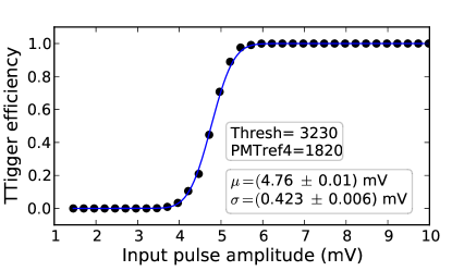
The trigger efficiency as a function of pulse amplitude, , for a particular configuration of the ASIC parameters is shown in Figure 15. We fit to the efficiency points a function of the form
| (1) |
where erf is the Gaussian error function, and and are the fit parameters which represent the trigger threshold and noise, respectively.
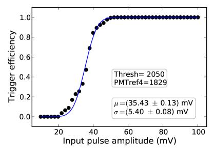
Figure 16 shows trigger threshold and noise from our scan of PMTref4 and Thresh.
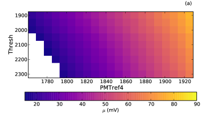
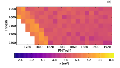
The minimum trigger threshold achievable in this mode (with analog sampling of the data path enabled) is mV, with a trigger noise mV, which correspond to 5 p.e. and 1.2 p.e., respectively, for a pre-amplifier with a gain of 4 mV per photoelectron. This performance does not meet the design goal of triggering on 2 photoelectrons with trigger noise below 1 photoelectron. The next paragraphs describe how we investigated the causes of this behavior.
3.3.2 Trigger performance for operations in sync with sampling
Since the input signal is going on one side to the trigger circuit, and, on the other side, to the sampling circuit that is the first stage of the data path, we wanted to study how the trigger performance depends on the sampling signals internal to the ASIC.
The input signal is sampled using as a reference a clock signal with a full period of 64 ns. For testing purposes, we extracted from the FPGA a signal synchronous with the sampling clock downscaled to a frequency of 119 Hz (generated every 512 full cycles through the 16,384 cells of the storage buffer). This signal was sent to the function generator as an external trigger, in order to generate pulses at fixed phase with respect to the sampling clock. We varied the delay between the external trigger to the function generator and the output pulse between 0 and 128 ns (2 full periods of the sampling clock), and evaluated for a given PMTref4-Thresh pair trigger threshold and noise as a function of this delay.
Figure 17 shows trigger threshold and noise from the delay scan.
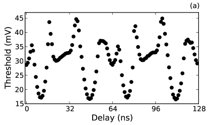
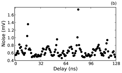
The threshold exhibits a pattern with 64 ns period, clearly indicative of some interplay between sampling and triggering. The variations in the threshold values are as large as mV. On the other hand, for operations in sync with the sampling clock the noise is typically mV, with larger values of a few mV in points where the threshold is rapidly changing. This demonstrates that the mV noise in normal (asynchronous) operations, shown Figures 15 and 16(b), is mostly due to threshold variations for pulses that arrive at different sampling phases.
Figure 18 shows a typical efficiency curve for operations in sync with sampling. The transition is much sharper, and in this case the function provides a much better fit to the data, which indicates that the deviations in normal mode are given by the superposition of many curves with different thresholds.
3.3.3 Trigger performance with sampling disabled
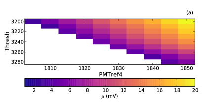
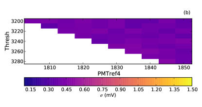
Because the performance of the trigger system is strongly dependent on the analog sampling, we characterized the trigger performance with sampling disabled. Figure 19 shows trigger threshold and noise from our scan in PMTref4 and Thresh when the sampling is disabled.
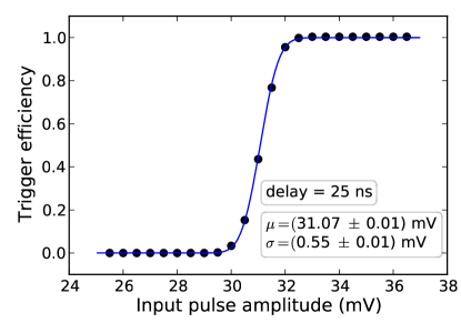
In this configuration, the minimum workable threshold is mV (1.2 p.e.), and the trigger noise is mV (0.13 p.e.). Figure 20 shows an efficiency curve for sampling disabled for which the threshold was 4.76 mV. Also in this casfe the measured efficiencies are well fit by an curve.
In conclusion, the performance of the trigger circuit with sampling disabled meets the desired sensitivity and noise level. Therefore, two options were considered: 1) reducing the interference on the ASIC between sampling and triggering circuits (by improving isolation and increasing the gain on the trigger path), 2) separating data and trigger path into two different ASICs. Option 1) was chosen as the most cost effective for the design of TARGET 7, and option 2) for subsequent ASIC pairs.
3.3.4 Trigger output
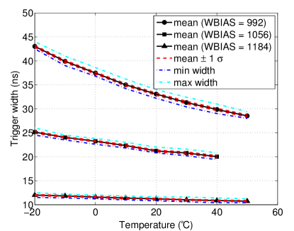
The trigger output signal characteristics are summarized in Figure 21. The output signal has 2 V amplitude and a width that is tunable using a control voltage (WBias). The chip produces pulses with stable width and amplitude for pulses as narrow as 10 ns. This width exhibits some temperature dependence, as shown in Figure 21. However, the temperature dependence is weak for narrow (10 ns) pulses that will be used for most applications.
The maximum sustained trigger rate achievable without event loss for a waveform length of 2 blocks, i.e., 64 samples, was measured to be kHz. The limit in the test setup is dominated by the UDP link and a prototype data acquisition software. Nevertheless, the readout rate achieved is larger than the rate of Hz expected for the GCT camera, and that of a few kHz expected for the SCT camera.
4 Front-end electronics module
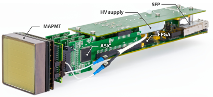
A front-end electronics module based on TARGET 5 has been designed and produced for a prototype CTA camera, CHEC-M [7, 8]. This camera is designed for use with Schwarzschild–Couder small-sized telescopes and features 32 TARGET 5 modules per camera, each reading out a 64-pixel MAPMT (which corresponds to 128 TARGET 5 ASICs per camera). 35 TARGET 5 modules were produced and are currently undergoing commissioning as part of the integrated camera. A module is shown in Figure 22. CHEC-M and its front-end electronics system will be described in more detail in subsequent publications.
5 Conclusion and outlook
We have developed a new ASIC of the TARGET family designed to read out signals from the photosensors in cameras of very-high-energy gamma-ray telescopes exploiting time-resolved imaging of Cherenkov light from air showers. TARGET 5 processes signals from 16 photodetector pixels in parallel both for sampling and digitization and for trigger formation.
Key aspects of the TARGET 5 performance are:
-
1.
sampling frequency tunable between GSa/s and GSa/s (Fig. 3)
-
2.
a dynamic range on the data path of 1.2 V with effective dynamic range 11 bits and DC noise mV (Fig. 6)
-
3.
3-dB bandwidth of 500 MHz (Fig. 10)
-
4.
crosstalk between neighboring channels (Fig. 11)
- 5.
-
6.
minimum stable trigger threshold of 20 mV (5 p.e.) with trigger noise of 5 mV (1.2 p.e.), mostly limited by interference between sampling and trigger operations (Fig. 15)
-
7.
minimum stable trigger threshold of mV (1.2 p.e.) with trigger noise of 0.5 mV (0.12 p.e.) with sampling disabled (Fig. 20)
TARGET 5 is part of the front-end electronics system of the first GCT camera prototype, also known as CHEC-M [7, 8], and is the first ASIC in the TARGET family to be used in an IACT prototype which is proposed in the framework of the CTA project.
To meet the performance desired for CTA, further developments are ongoing that are briefly outlined in [12].
Acknowledgements
This research was supported by the SLAC LDRD Grant “Integrated TeV Gamma-ray Camera Readout System” and by the Stanford University Dean’s Grant “Cherenkov Telescope Array”, as well as by JSPS KAKENHI Grant Numbers 25610040 and 23244051. A. O. was supported by a Grant-in-Aid for JSPS Fellows. Additional support to J. V. and T. W. was provided by the University of Wisconsin.
We are grateful for many fruitful discussions with members of the CTA consortium, in particular of the GCT and SCT groups. We are especially grateful for assistance in evaluating and optimizing the ASIC performance by Sonia Karkar, and for feedback on the measurements and paper draft from Felix Werner and Scott Wakely.
This paper has gone through internal review by the CTA Consortium.
References
- [1] J. A. Hinton, W. Hofmann, Teraelectronvolt Astronomy, ARAA47 (2009) 523–565. arXiv:1006.5210, doi:10.1146/annurev-astro-082708-101816.
- [2] M. Actis, G. Agnetta, F. Aharonian, A. Akhperjanian, J. Aleksić, E. Aliu, D. Allan, I. Allekotte, F. Antico, L. A. Antonelli, et al., Design concepts for the Cherenkov Telescope Array CTA: an advanced facility for ground-based high-energy gamma-ray astronomy, Experimental Astronomy 32 (2011) 193–316. arXiv:1008.3703, doi:10.1007/s10686-011-9247-0.
- [3] V. Vassiliev, S. Fegan, P. Brousseau, Wide field aplanatic two-mirror telescopes for ground-based -ray astronomy, Astroparticle Physics 28 (2007) 10–27. arXiv:astro-ph/0612718, doi:10.1016/j.astropartphys.2007.04.002.
- [4] M. Wood, T. Jogler, J. Dumm, S. Funk, Monte carlo studies of medium-size telescope designs for the cherenkov telescope array, Astroparticle Physics 72 (2016) 11 – 31. doi:http://dx.doi.org/10.1016/j.astropartphys.2015.04.008.
- [5] K. Bechtol, S. Funk, A. Okumura, L. L. Ruckman, A. Simons, H. Tajima, J. Vandenbroucke, G. S. Varner, TARGET: A multi-channel digitizer chip for very-high-energy gamma-ray telescopes, Astroparticle Physics 36 (2012) 156–165. arXiv:1105.1832, doi:10.1016/j.astropartphys.2012.05.016.
- [6] T. Montaruli, G. Pareschi, T. Greenshaw, The small size telescope projects for the Cherenkov Telescope Array, in: Proceedings of the 34th International Cosmic Ray Conference, Vol. POS(ICRC2015)1043, 2015. arXiv:1508.06472.
- [7] M. K. Daniel, R. J. White, D. Berge, J. Buckley, P. M. Chadwick, G. Cotter, S. Funk, T. Greenshaw, N. Hidaka, J. Hinton, J. Lapington, S. Markoff, P. Moore, S. Nolan, S. Ohm, A. Okumura, D. Ross, L. Sapozhnikov, J. Schmoll, P. Sutcliffe, J. Sykes, H. Tajima, G. S. Varner, J. Vandenbroucke, J. Vink, D. Williams, f. t. CTA Consortium, A Compact High Energy Camera for the Cherenkov Telescope Array, in: Proceedings of the 33rd International Cosmic Ray Conference, 2013. arXiv:1307.2807.
- [8] A. De Franco, R. White, D. Allan, T. Armstrong, T. Ashton, A. Balzer, D. Berge, R. Bose, A. M. Brown, J. Buckley, P. M. Chadwick, P. Cooke, G. Cotter, M. K. Daniel, S. Funk, T. Greenshaw, J. Hinton, M. Kraus, J. Lapington, P. Molyneux, P. Moore, S. Nolan, A. Okumura, D. Ross, C. Rulten, J. Schmoll, H. Schoorlemmer, M. Stephan, P. Sutcliffe, H. Tajima, J. Thornhill, L. Tibaldo, G. Varner, J. Watson, A. Zink, The first GCT camera for the Cherenkov Telescope Array, 2015. arXiv:1509.01480.
- [9] A. N. Otte, J. Biteau, H. Dickinson, S. Funk, T. Jogler, C. A. Johnson, P. Karn, K. Meagher, H. Naoya, T. Nguyen, A. Okumura, M. Santander, L. Sapozhnikov, A. Stier, H. Tajima, L. Tibaldo, J. Vandenbroucke, S. Wakely, A. Weinstein, D. A. Williams, f. t. CTA Consortium, Development of a SiPM Camera for a Schwarzschild-Couder Cherenkov Telescope for the Cherenkov Telescope Array, in: Proceedings of the 34th International Cosmic Ray Conference, Vol. POS(ICRC2015)932, 2015. arXiv:1509.02345.
- [10] G. Varner, L. Ruckman, P. Gorham, J. Nam, R. Nichol, et al., The large analog bandwidth recorder and digitizer with ordered readout (LABRADOR) ASIC, Nucl.Instrum.Meth. A583 (2007) 447–460. arXiv:physics/0509023, doi:10.1016/j.nima.2007.09.013.
- [11] D. Casadei, Estimating the selection efficiency, Journal of Instrumentation 7 (2012) 8021. arXiv:0908.0130, doi:10.1088/1748-0221/7/08/P08021.
- [12] L. Tibaldo, J. A. Vandenbroucke, A. M. Albert, et al., in: Proceedings of the 34th International Cosmic Ray Conference, Vol. POS(ICRC2015)932, 2015. arXiv:1508.06296.