Electron-acoustic-phonon interaction in core/shell Ge/Si and Si/Ge nanowires
Abstract
General expressions for the electron- and hole-acoustic-phonon deformation potential Hamiltonians () are derived for the case of Ge/Si and Si/Ge core/shell nanowire structures (NWs) with circular cross section. Based on the short-range elastic continuum approach and on derived analytical results, the spatial confinement effects on the phonon displacement vector, the phonon dispersion relation and the electron- and hole-phonon scattering amplitudes are analyzed. It is shown that the acoustic displacement vector, phonon frequencies and present mixed torsional, axial, and radial components depending on the angular momentum quantum number and phonon wavevector under consideration. The treatment shows that bulk group velocities of the constituent materials are renormalized due to the spatial confinement and intrinsic strain at the interface. The role of insulating shell on the phonon dispersion and electron-phonon coupling in Ge/Si and Si/Ge NWs are discussed.
pacs:
62.23.Hj,63.20.D-,63.20.kdI Introduction
Based on enforcement of Si nanowires (NWs) linked to thermal conductivity, Khitun et al. (1999) photodetectors Servati et al. (2007) and solar cells, Tian et al. (2007); Murphy-Armando et al. (2010); Hochbaum et al. (2005) nowadays a notable effort has been addressed to study Si/Ge and Ge/Si core/shell semiconductor NWs. Peng and Logan (2010); Wingert et al. (2011); Hu et al. (2011a); Amato et al. (2014) These typical type-II band structures display high mobility Kagimura et al. (2007) and can be used in many applications. Yang et al. (2008); Peng et al. (2011a); Huang and Yang (2011) It is also well established that the band gap at -point of core/shell Si/Ge and Ge/Si nanostructures increases with decreasing radius, an effect directly linked to the spatial confinement and to the intrinsic strain at the interface, Peng et al. (2011a); Logan and Peng (2009) produced in turn by the 4% lattice mismatch between Si and Ge materials. Zhao et al. (2004) Yet, more interestingly, in the nanoscale regime the Si/Ge and Ge/Si core/shell structures show a direct band gap at -point. Beckman et al. (2006); Medaboina et al. (2007); Peng and Logan (2010)
Besides the intrinsic strain, it is important to considered the role of spatial confinement on the acoustic-phonon modes and on the electron-phonon interaction. The acoustic phonon dispersion is strongly modified Pokatilov et al. (2005) when the radius of the quantum wire is of the order or smaller than the phonon wavelength. The confined acoustic phonon in such a nanostructure plays an important role on the carrier scattering rate, on the flow of electric current, and on the mobility or carrier transport. A suppression of the thermal conductivity in the core/shell Si/Ge NWs has been reported in Refs. Nika et al., 2011, 2012, 2013. It has been shown that certain combinations of the core/shell cross-section modulation and the acoustic mismatch allow to control the thermal flux. This result is, in principle, a promissory candidate for thermoelectric applications. Thus, the reduction of the thermal conductivity and the characteristic of the carrier mobility in core/shell NWs are directly linked to the confinement effects on the phonon dispersion relation. Yang et al. (2005); Chen et al. (2012); Neophytou and Kosina (2010); Tienda-Luna et al. (2013); Nika et al. (2013) Also, it is important to remark that the core/shell wire structures are useful for optical applications Treu et al. (2013); Mayer et al. (2013) and for quantum computing engineering with spin qubits. Hu et al. (2011b); Higginbotham et al. (2014)
Several works have been devoted to obtain the acoustic phonon dispersion in wires and core/shell nanowires using both ab initio calculations Peelaers and Peeters (2012); Peelaers et al. (2010) and phenomenological continuum approaches (see Refs. Pokatilov et al., 2005; Huang and Kang, 2011; Kloeffel et al., 2014; Fomin and Balandin, 2015 and references there in). In addition, studies of electron-phonon interaction for the conduction band have been reported. Hattori et al. (2010); Buin et al. (2008); Yu et al. (1995) However, the electron-acoustic-phonon interaction in core-shell NWs has not been fully tackled. A phenomenological theory, allowing for the evaluation of the electron-phonon Hamiltonian due to a deformation potential interaction, for cylindrical structures with arbitrary radii for both core and shell at the nanoscale regime, is a central issue for understanding the fundamental physics of many of the phenomena aforementioned. In the present work we study the electron-phonon interaction in Ge-core/Si-shell and Si-core/Ge-shell NWs in the framework of the continuum model and the band theory.
The paper is organized as follows: in Sec. II we write down the general expression for the electron- and hole-phonon deformation-potential Hamiltonians. For the conduction band we assume the symmetry to be valid for Ge/Si and Si/Ge NWs grown along [110], while for the holes we adopt the Bir-Pikus Hamiltonian (BPH) for states near the top of the valence bands with symmetry. Sec. III is devoted to a description of the elastic continuum model and the general basis of solutions for the phonon amplitudes. We make special emphasis on the phonon spectrum calculations, the role of the spatial confinement effect, the symmetry of the space of solutions and on the comparison with the homogeneous wire limit. In Sec. IV we present detailed derivations of the electronic-acoustic phonon scattering rate for conduction and valence bands and of the influence of the core and shell radii for electrons and holes on the scattering amplitudes. We report our main results in Sec. V. Finally, in the Appendices we summarize the most relevant technical elements in the development of the present work.
II Electron-acoustic-phonon interaction
We consider typical core/shell cylindrical NWs with core radius , shell thickness , and the axis parallel to the growth direction [110]. We assume that all parameters involved in the present theoretical model are piece-wise functions of , that is, we have assumed the parameters of the constituent materials to be isotropic.
In the occupation number representation, the Hamiltonian of the electrons interacting with the acoustic phonons can be expressed as Madelung (1996)
| (1) |
where () denotes the phonon creation (annihilation) operator in the branch with wavevector and (), the corresponding operator for electron in the electronic state (). Here, takes into account the electronic scattering event between the states by the interaction with an acoustic phonon. It is well known that in Si and Ge semiconductors the electron-phonon coupling can be determined using the short range deformation potential (DP) model. Yu and Cardona (2010) In a first approach, we develop a theory where this interaction is treated in the same way as in the bulk DP approach. Nevertheless, it has been reported that the DP constants are anisotropic and that depend on the spatial confinement (see Ref. Murphy-Armando et al., 2010 and references there in). Furthermore, the DP mechanism can be treated as a perturbation to the band energies due to the lattice distortion; as a consequence, the electron-phonon coupling depends on the electronic band structure. Yu and Cardona (2010) As we stated above, the Ge/Si and Si/Ge core/shell nanowires grown in the [110] direction show a direct band gap at -point of the Brillouin zone, Beckman et al. (2006); Arantes and Fazzio (2007); Medaboina et al. (2007); Peng et al. (2011a) hence, the conduction band minimum shows a symmetry, while the top valence band has a one, respectively.
II.1 Conduction band
Following the above discussion, the electron-phonon scattering amplitude probability can be written as
| (2) |
where is the volume deformation potential, Yu and Cardona (2010) is the phonon displacement vector in the branch , and is the electron wave function for the core/shell NW.
II.2 Valence band
For the scattering amplitude, , of a hole in the valence band interacting with an acoustic phonon we have
| (3) |
where is the hole wave function in the NW and is the Bir-Pikus Hamiltonian for the valence band states. Bir and Pikus (1974); Yu and Cardona (2010) Assuming the zinc-blende symmetry, the Hamiltonian in cylindrical coordinates and in the framework of the axial approximation, can be written as
| (4) |
with and being the volume and shear deformation potentials for the highest energy at valence band, Not (a) , , and the Cartesian angular momentum operators for a particle with spin 3/2 and the components of the stress tensor (see Appendix A Eq. (22)).
III Acoustic-phonon dispersion
For an evaluation of the Hamiltonian (1) and, in consequence, the matrix elements (2) and (3), it is necessary to know the dependence of the phonon displacement as well as the phonon frequencies on the core/shell spatial symmetry. In the framework of elastic continuum approach, the equation of motion for the acoustic phonon modes takes the form Born and Huang (1988)
| (5) |
with the mass density, the phonon frequency and the mechanical stress tensor. Following Hooke’s law, , with the strain tensor, the elastic stiffness tensor and the results being compiled in the Appendix A, the equation of motion for the acoustic phonon takes the form
| (6) |
The solution of (6) consists of one longitudinal () and two transverse () fields, i.e. . Since the system is not homogeneous, in general , , are coupled by the matching boundary conditions at the interface. Thus, the acoustic dispersion relations for the L and T branches are not independent and the normal modes become a hybrid combination of , and phonon vibrational motions.
It is important to remark that the equation of motion (6) for , or , corresponds to an isotropic model where an average velocity for the sound is assumed. An analysis of the phonon calculations and more general expressions including the anisotropy are presented in Appendix A. It is shown there the phonon frequency calculations present a discrepancy of in comparison with the isotropic model.
In cylindrical geometry, the solution of Eq. (6) has full axial symmetry; hence, the displacement vector in cylindrical coordinates can be cast as . In consequence, and following the method of solution described in Refs. Trallero-Giner et al., 1998; Santiago-Pérez et al., 2015, one can derive a general basis of solutions for , namely
| (7) |
where labels for the azimuthal motion, is the -component of the phonon wavevector, and is given by
| (8) |
In Eq. (7), if the function is taken as Bessel (or Infeld for and as linear combination of and Neumann functions of integer order (or combination of and MacDonald ) Abramowitz and Stegun (1964) for . From (7), it is easy to check that (sign + for the Bessel functions and - for the modified Bessel functions) with and , underlying the transverse and longitudinal character of the fields , and .
The eigenfrequencies of the phonon modes are obtained by imposing appropriate boundary conditions. As in the case of optical phonons, the strains at the interface play an important role on the phonon frequencies (see Ref. Singh et al., 2011). For the acoustic phonons, the effects of lattice mismatch between Ge and Si are taken into account through the continuity of the normal component of the stress tensor. We consider a free boundary at the shell surface, . Besides, the mechanical displacement and the normal component of the stress tensor should be continuous at the core/shell interface, i.e. and . We point out that in the case of free standing homogeneous nanowires the basis of solutions (7) match those reported in Ref. Hattori et al., 2010.
The calculation for the acoustical modes in NWs with cylindrical symmetry is a complicated task. In general, the phonon displacement has all three components (, and ), since none of the coefficients , and is zero, therefore, it cannot be decoupled into independent motions. Fixing and , the constants , and are fully determined by the matching condition at and by the boundary condition of free standing NWs at . Due to the cylindrical symmetry we cannot characterize the motions as pure torsional, dilatational or flexural modes. The resulting modes are combination of transverse and longitudinal characters. Nevertheless, from the symmetry of general basis (7) we are able to obtain the following results: (i) for and , we are in the presence of three independent , and uncoupled modes with amplitudes , and , respectively; (ii) for and , the longitudinal and transverse motions, , are coupled, while vibrational mode remains uncoupled; (iii) for and , the transverse phonon mode is independent, while the other two, and , are mixed; (iv) for and the longitudinal, the transverse and motions are coupled. Below, we focus on the most relevant case of phonons with axial symmetry, .
III.1 Phonons with
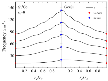
As stated above, the present case shows three uncoupled vibrations, , and . The longitudinal modes correspond to radial breathing mode (RBM) and their eigenfrequencies are ruled by the secular equation
| (9) |
where labels the core (shell) region, , , , , , and (). The RBM modes have been studied in the past for both nanotubes Maultzsch et al. (2005); Kürti et al. (2003) and semiconductor NWs. Bourgeois et al. (2010); Trejo et al. (2013) Because of their particular relevance it becomes necessary to focus on these modes in Ge/Si and Si/Ge core/shell nanowires. It is expected that the frequencies of the RBM modes, described by Eq. (9), are strongly dependent on the material composition, and size ratio, . Firstly, note from (9) that the two limiting cases and are given by the secular equation with () and the radius of the wire, i.e. the homogeneous NW dispersion relation is recovered for shell or core semiconductors. Figure 1 shows the frequency dependence on the core/shell ratio , with the limiting cases and shown by diamonds. In the calculations we employed the following data for Si [Ge]: , , Not (b) . Adachi (2005) The oscillations observed in Fig. 1 of as a function of the ratio can be explained by the interference between shell and core structures. Thus, for small values of , the influence of the shell on the core phonon amplitude becomes stronger inhansing the oscillations. Moreover, the lower phonon frequencies are less affected showing almost a flat dispersion as a function of , while the higher excited modes are more sensitive and displaying pronounced oscillations. The same trend is obtained for the and phonon modes (see Fig. 2).
The confined eigenfrequencies, , for the modes can be obtained from the general expression
| (10) |
Here, , and . Also, in the particular case when , is possible to get an explicit expression for the frequency mode.
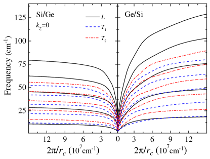
Figure 2 displays the dependence on of the uncoupled , and phonon frequency modes for fixed shell thickness . In the limit we recover the phonon frequencies for pure Si and Ge wires. As , we find that the phonon frequency resembles the typical linear acoustic bulk phonon dispersion as a function of the phonon wavevector. The spatial confinement renormalizes the sound velocity and we can rewrite, for large values of , that () with different slope for each mode. Notice that the cylindrical symmetry breaks the and degeneracy and two different sound velocities, and , appear.
III.2 Phonon dispersion with
Following the secular Eq. (10), in Fig. 3 we display the pure confined transverse phonon dispersion. For sake of comparison the bulk phonon dispersions, and , are represented by blue and red dashed lines, respectively. For small values of is possible to get useful analytical solutions. It should be remarked that in the case of Ge/Si, if the set of the values ( lies in the region , the parameter is real while becomes a complex number. The opposite occur for Si/Ge NWs. Accordingly, for the Ge/Si we get that the function .
The numerical solution of Eq. (10) shows a strong modification of the Si and Ge bulk phonon group velocities (see Fig. 3) which depend on the surrounding material, i.e. if the shell is composed by softer or harder material than the core semiconductor, the resulting group velocity has lower or higher values. For example, in Ge/Si core/shell NWs the shell compresses the Ge core lattice while for Si/Ge the shell is compressed by the core. Similar result have been achieved in Ref. Pokatilov et al., 2005.
Assuming small values of the wavenumber , Eq. (11) is obtained from Eq. (10). Thus, the dispersion relation valid for Ge/Si ( real, complex number) and Si/Ge ( complex number, real) follows. This enables to better visualize the dependence of sound speed on materials parameters:
| (11) |
This equation shows that the lower modes present linear dependence in , with a renormalized sound velocity that takes into account the ratio between shell and core radii, as well as the densities and transverse velocities. Equation (11) suggests the way to modify the sound velocity as a function of the geometric factors ranging between the values and . The same expression has been found in Ref. Kloeffel et al., 2014.
In the domain ( where and are both real functions, Eq. (10) provides the dispersion relation for small values of ,
| (12) |
where is the confined phonon frequency of the core/shell NWs for . In Fig. 3 the solutions given by Eqs. (11) and (12) are represented by open diamonds. By comparison with the numerical calculation of Eq. 10), it can be seen that explicit expressions (11) and (12) are good approximations for .
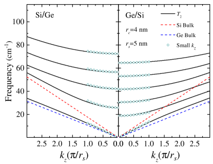
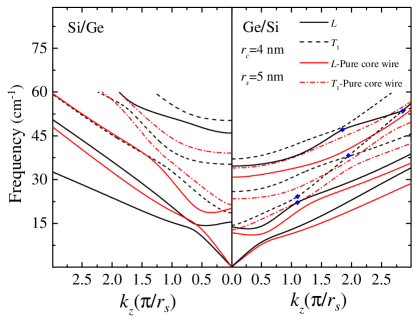
Another subset of solutions corresponds to the hybridized longitudinal and transverse motions. Fig. 4 shows phonon dispersion of mixed modes for . The longitudinal () and transverse () labels are taken from the character of the mode at . For the sake of comparison, the phonon dispersions for the homogeneous Si and Ge cylindrical wires are shown in Fig. 4. Here, the corresponding longitudinal and transverse modes are represented by red solid and red dash-dots lines, respectively. Due to the strain effect at the interface, it can be seen in the Fig. 4 that for the Ge/Si core/shell NW the phonon frequencies lye above the Ge wire, while the opposite is obtained for the Si/Ge NW, where values are well above the core/shell Si/Ge phonon frequencies. At approaching zero, the lower mode presents a linear dependence of on the wavenumber with certain effective sound velocity that depends on the radii and . Not (c, d) The bendings appearing in the Fig. 4 are manifestations of the strongest coupling between and modes. The mixed character of the states avoid crossing points in the phonon dispersion relation, i.e. the repulsion between near modes with the same symmetry occurs. This effect is observed in all dispersion relations having an important consequence in the electron-phonon Hamiltonian (see discussion below). In Fig. 4, some anticrossings associated with the mixing between and states, have been indicated by full diamonds. The proximity of the levels belonging to the same space of solution or with the same symmetry is avoided by the repulsion between the phonon states. At the anticrossings, a strong mixing between and states occurs and an exchange of character of the constants and is obtained as a function of .
Notice that higher excited states for do not present strong mixing effect and the phonon dispersion relation can be described by simple parabolic law, . Here, measures the curvature of the phonon dispersion and are the NW phonon frequencies for . We arrived to the same results for the homogeneous Si and Ge cylindrical wires.
IV Scattering rate
Due to translational and cylindrical symmetries, the matrix element can be cast as follows
| (13) |
where the angular momentum and linear momentum conservations are written explicitly. is the scattering amplitude due to the electronic transition assisted by an acoustical phonon, between the electron or hole states (see Appendices B and C). For the phonon eigenvectors we choose the normalization condition
| (14) |
with the acoustic-phonon dispersion of the core/shell problem. Let us discuss a general formulation for the electron-acoustic deformation potential Hamiltonian, and an evaluation of the scattering amplitudes for the electrons and holes.
IV.1 Electron-LA Hamiltonian
According to Eq. (2), a transverse or torsional mode does not induce volume change and only the longitudinal acoustic motion contributes to electron-phonon Hamiltonian . Hence, by assuming as independent constant in Eq. (7), we have
| (15) |
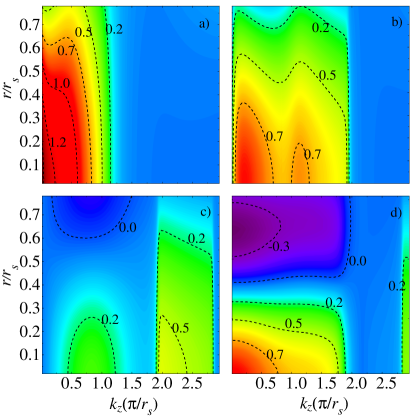
where is the normalization constant for the dimensionless phonon amplitude . In Fig. 5 the characteristic contour map for the electron-LA Hamiltonian (15) is shown for the Ge/Si NWs. We choose the first four modes of Fig. 4 where . According to the general basis of solutions (7), for , the longitudinal displacement vector have non-zero radial and axial components. Figures 5 a), b), c) and d) correspond to the uncoupled confined frequencies , , , and for of the and motions. In the panels a) and d) one finds, for , the stronger spatial localization in correspondence with the longitudinal character of these modes. In panel a) we observe, as increases, that the component becomes stronger, in particular for the contribution of the mode to is almost zero. The same is observed in panel d) for the state , but the limiting value is . These two values of are in correspondence with the anticrossings shown by full diamonds in the Figure 4 for the and phonon states. Note in Fig. 4 that for an anticrossing occurs and the mode presents stronger character and, in consequence, the spatial distribution of is enhanced. In panel b) the observed strong spatial localization of at with is explained by the reduction of the coefficient as a function of , in the state . Due to the anticrossing between the states and for , the mode is almost transverse and its contribution to the spatial distribution decays to zero. At the same time, the mode increases the amplitude, and at increases in the region as seen in Fig. 5c). Thus, the phonon dispersion of the Ge/Si NWs for a given ratio of has a preponderant influence on the spatial distribution of as a function of .
Taking into account the Eqs. (15), (30) and (41), the electron scattering amplitude can be written as
| (16) |
where . From Eq. (16) immediately follows that phonon modes with assist to electron intrasubband transitions, , while for intersubband transitions with occur fo. Note that in the case of homogeneous wire, corresponds to the electron form factor or overlap integral between the normalized radial electronic states and the phonon function of the quantum wire. For comparison, we consider the Eq. (16) for a homogeneous wire. Assuming the size-quantum limit (strong spatial confinement) where electrons populate the lowest subband and and intersubband transitions are discarded, the scattering amplitude at reduces to
| (17) |
with .
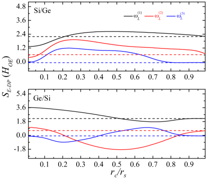
It is instructive to compare the behavior of the electron scattering amplitudes for core/shell Si/Ge and Ge/Si NWs. Fig. 6 displays the reduced scattering amplitude as a function of the ratio for both core/shell NWs. In the calculation for the Si/Ge [Ge/Si] NWs we fixed the value of with the parameters of Si [Ge] semiconductor. For each structure, in the quantum limit approach, the first three modes of the structure with frequencies () at are considered. In the figure the form factor, using Eq. (17) and nm, is represented by dashed lines. In Si/Ge NWs, electrons are confined in the core whereas in Ge/Si NWs they are in the shell. For the evaluation of Eq. (16) we employed the results displayed in Appendix B. In the upper panel of Fig. 6 (Si/Ge NWs) the influence of the shell of Ge on the is shown. If we have a quantum wire of Si and as described by Eq. (17). If we are in the presence of a Si/Ge core/shell system. Thus, we can observe that the value of , for the modes, firstly increases, reaching a maximum for and for the quantity reaches asymptotically the homogeneous Si wire value. In the case of (), the reduced scattering amplitude grows, reaching a maximum value near (. For , decreases to the limiting value of Eq. (17). In the lower panel of Fig. 6 (Ge/Si NWs) the wire of Ge is reached at . From the figure we can observe the strong influence of the shell on the for besides oscillations of around the values, a fact reflecting the oscillatory behavior of the phonon modes with (see Fig. 1). A similar result for the electron scattering amplitude has been reported in Ref. Ramayya et al., 2008 for Si nanowires.
IV.2 Hole-Acoustical-Phonon Hamiltonian
By employing the solutions for the phonon amplitudes (7), the matrix representation of the angular momentum Luttinger (1956); Kloeffel et al. (2011) and the strain relations given in Appendix A, the hole scattering amplitudes for the Hamiltonian (4) can be cast as
| (18) |
where , , ,
| (19) |
| (20) |
From Eqs. (18), (20) and the basis of solutions (7), we extract the following conclusions: a) For phonon states with and we have three independent hole-phonon interaction Hamiltonians, accounting for the three uncoupled subspaces, , , , with eigenfrequencies , and , respectively. Evaluating (20) at and using the fact that and , we see that the Hamiltonian (18) couples the diagonal intraband hole sates and the weak coupling interband between states; if we choose where and , we are in the presence of interband transitions . Also, for with and , results in scattering . b) Fixing and there are two independent subspaces, and . The first one couples and motions, while the second corresponds to pure transverse phonons. Similar expressions are obtained for homogeneous wires by choosing properly the function and inside the cylinder.
In the size-quantum limit and not too large values of , the Luttinger-Kohn (LK) Hamiltonian splits into two independent matrices, coupling (, or (, Bloch states (see Appendix C). For and angular momentum quantum number , the scattering amplitude (19) splits into two independent terms, which correspond to the subspaces and of the hole-phonon interaction Hamiltonian.
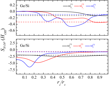
Figure 7 is devoted to the hole scattering amplitude (19) in units of for the first three transverse modes (upper panel) and three longitudinal modes (lower panel) of the Ge/Si structure as a function of the ratio . In the calculation we assumed that the lower hole state is completely confined in the core (hard wall potential approximation). As in Fig. 6, dashed lines represent the form factor for Ge NW with a radius of 5 nm. Here, the influence of the shell is solely due to Ge/Si phonon spectrum. From the figure we observe that for the longitudinal modes are one order of magnitude larger than the transverse ones, reflecting the strength of coupling between hole states. In the case of we have a coupling between and , while for the we are in the presence of the diagonal transitions and . Another feature is the strong oscillation of the for transverse modes with respect to the phonons. The vibrations couple the cylindrical function of second order, while for the modes, is proportional to the Bessel function . In addition, a useful result can be extracted from Fig. 7, that is, we can obtain the minimum value of where the hole-phonon Hamiltonian for core/shell NWs can be considered as a pure Ge wire. Notice that this result depends on the type of interaction; for modes: and for modes: .
V Conclusion
In summary, we have studied the acoustical phonon dispersions, the phonon displacement vectors and the electron- and hole-acoustical phonon Hamiltonians in core/shell Ge/Si and Si/Ge NWs. Our results show the influence of the core radius and shell thickness of Si-Ge based nanowires on the phonon frequencies and electron-phonon and hole-phonon interaction Hamiltonians. Due to the presence of the shell, the phonon frequencies exhibit oscillations as function of the ratio leading to a strong influence on the interaction Hamiltonians and scattering amplitudes. The gapless phonons have a tuned renormalized group sound velocities in terms of the geometrical factor . Also, it is shown that scattering amplitudes for the conduction and valence bands can be handled by the shell thickness. The obtained results can be viewed as a basic tool for exploration of electron and hole transport phenomena and Brillouin light scattering, as well as for device applications of these one-dimensional Ge/Si and Si/Ge core/shell nanostructures. The systematic derivation and explicit, relatively simple, solutions of the electron and Bir-Pikus hole deformation potential Hamiltonians, incorporating the characteristics of the phonon modes for the wavenumber , present straight applications to the resonant Raman scattering processes in core/shell NWs. Thus, searching at different light scattering configurations of the Brillouin and Raman processes, it possible to study the dependence of the and phonon modes on the spatial confinement and the intrinsic stress at the interface.
Appendix A Stress tensor
For Ge and Si semiconductors with diamond structure, the relation between stress and strain, , in cylindrical coordinates, can be written as
| (21) |
where the are the elastic stiffness coefficients and the components of the strain tensor in terms of the phonon displacement vector are given by
| (22) |
Considering isotropic bulk materials the acoustic phonon branches at -point are degenerate and we have that , and with the transverse (longitudinal) sound velocity. Accordingly the stress tensor is reduced to
| (23) |
where is the identity matrix. In general the vibrational modes are anisotropic along different crystallographic directions. To carried out the effect of anisotropy we must modify the isotropic continuum model (23) including the complete form of the stress tensor. We can write , where is given by Eq. (23) with and for we have
| (25) |
and . Taking advantage of the fact that the relation and 0.24 for Si and Ge, respectively, we can consider the tensor as small perturbation relative to . Following the procedure developed in Ref. Trallero-Giner et al., 1998 and Chamberlain et al., 1994 we obtain the frequencies of the modes including the anisotropy as , where
| (26) |
Here, and represent the eigenfrequency and eigenvector solution of Eq. (5) and the operator being defined as
| (28) | |||||
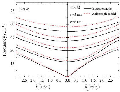
with . Using Eq. (26) we obtain for the modes along [110] direction with and that the anisotropy does not affect the longitudinal modes and , while for the transversal and modes, are shifted in comparison to the isotropic case for both Ge/Si and Si/Ge NWs. Figure 8 displays the effect of the anisotropy on the decoupled () phonon spectrum for Si/Ge and Ge/Si NWs. The solid lines represent the calculation assuming the isotropic model while the anisotropic case is shown by red dashed lines. In both NWs we observe a upshift, less than , from the frequency modes with the correction (26). Similar calculations can be performed for any crystallographic direction and phonon modes.
Appendix B Electron wave function
In the framework of the Envelope Function Approximation, the electron wave function in cylindrical symmetry can be written as
| (30) |
where is the core volume, the normalization length, and are the -component of the angular momentum and electron wavenumber, respectively, and the radial wave function. Considering bound states, we are in presence of two cases: Yang et al. (2008); Peng and Logan (2010)
a) Si/Ge NW, where the states are confined in the core. Hence, it is possible to show that
| (31) |
with
| (32) |
| (33) |
and
| (34) |
b) In the case of For Ge/Si core/shell, the electronic states are localized in the shell and the above equations are reduced to
| (35) |
with the coefficients equal to
| (36) |
| (37) |
and
| (38) |
As stated above, labels the core (shell) semiconductor and is related to the electron energy by the equation
| (39) |
with and ( the longitudinal (transverse) conduction electron mass at -point of the Brillouin zone. Not (e) In Eq. (39) takes into account the gap energy correction due to the intrinsic strain at the interface Herring and Vogt (1956); Sun et al. (2007) and is the band offset between the core and shell measured from the bottom of the band. For NWs along [110] growth direction, the band gap meV. Yang et al. (2008) In our calculations we have assumed independent of .
There is a third option, not considered here, where both, and are real, and the radial wave function presents an oscillatory behavior in both the core and shell parts, which correspond to higher excited states of the core/shell NWs.
Appendix C Hole wave function
For a description of the hole states in the valence band we consider the LK Hamiltonian model neglecting the coupling from the split-off band. This Hamiltonian provides a good description for heavy-hole and light-hole states and the coupling between them due to degeneracy of valence bands at -point. Along the [110] direction and assuming the axial approximation, , the Hamiltonian can be written as Luttinger and Kohn (1955); Luttinger (1956); Rössler (1984)
| (40) |
where
| (41) | |||||
, , , , and are the Luttinger parameters. The total Hamiltonian for the valence band can be cast as with the NWs confinement potential. The wave function , as given by Eq. (30), represents a basis for the effective LK-Hamiltonian. Since the Bloch states, , , and are mixed by the effects of the cylindrical symmetry and the non-zero matrix elements and in Eq. (41), we can write the general solution of the wave function with a special sequence of the angular quantum number for each hole state. Thus, by exploring the symmetry of the Hamiltonian (40), the exact wave function for the hole state can be written as
| (42) |
where is related to the heavy (light) hole energy by the expression
| (43) |
and . As in the case of the conduction band in we consider the band gap correction. The vector coefficients ( in (42) are Sercel and Vahala (1990)
where the wight coefficients , , , give a measure of the mixtures of Bloch states , , and . Imposing continuity of the wave function and its derivative at the core/shell interface and choosing the boundary condition , we find the normalized eigensolutions and eigenenergies for the hole states.
In the case of Ge/Si core/shell NWs, the hole are mostly confined in the core and the valence band offset is of the order 0.5 eV. Yang et al. (2008); Peng and Logan (2010); Park et al. (2010) Thus, in the limit of strong spatial confinement we can assume a hard wall potential and the holes are completely confined in the core.
In the evaluation of the hole energy and wave function we employed for Si[Ge] the values , , , eV and eV. Adachi (2005)
Acknowledgements.
C. T-G and G. E. M acknowledge support from the Brazilian Agencies FAPESP (proceses: 2015/23619-1, 2014/19142-2) and CNPq. V. Romero is acknowledged for critical reading of the manuscript. D.S-P wishes to thank the CNPq-CLAF program for financial support.References
- Khitun et al. (1999) A. Khitun, A. Balandin, and K. Wang, Superlattices and Microstructures 26, 181 (1999), ISSN 0749-6036.
- Servati et al. (2007) P. Servati, A. Colli, S. Hofmann, Y. Fu, P. Beecher, Z. Durrani, A. Ferrari, A. Flewitt, J. Robertson, and W. Milne, Physica E: Low-dimensional Systems and Nanostructures 38, 64 (2007).
- Tian et al. (2007) B. Tian, X. Zheng, T. J. Kempa, Y. Fang, N. Yu, G. Yu, J. Huang, and C. M. Lieber, Nature 449, 885 (2007).
- Murphy-Armando et al. (2010) F. Murphy-Armando, G. Fagas, and J. C. Greer, Nano Letters 10, 869 (2010).
- Hochbaum et al. (2005) A. I. Hochbaum, R. Fan, R. He, and P. Yang, Nano Letters 5, 457 (2005).
- Peng and Logan (2010) X. Peng and P. Logan, Applied Physics Letters 96, 143119 (2010).
- Wingert et al. (2011) M. C. Wingert, Z. C. Y. Chen, E. Dechaumphai, J. Moon, J.-H. Kim, J. Xiang, and R. Chen, Nano Letters 11, 5507 (2011).
- Hu et al. (2011a) M. Hu, K. P. Giapis, J. V. Goicochea, X. Zhang, and D. Poulikakos, Nano Letters 11, 618 (2011a).
- Amato et al. (2014) M. Amato, M. Palummo, R. Rurali, and S. Ossicini, Chemical Reviews 114, 1371 (2014).
- Kagimura et al. (2007) R. Kagimura, R. W. Nunes, and H. Chacham, Phys. Rev. Lett. 98, 026801 (2007).
- Yang et al. (2008) L. Yang, R. N. Musin, X.-Q. Wang, and M. Y. Chou, Phys. Rev. B 77, 195325 (2008).
- Peng et al. (2011a) X. Peng, F. Tang, and P. Logan, Journal of Physics: Condensed Matter 23, 115502 (2011a).
- Huang and Yang (2011) S. Huang and L. Yang, Applied Physics Letters 98, 093114 (2011).
- Logan and Peng (2009) P. Logan and X. Peng, Phys. Rev. B 80, 115322 (2009).
- Zhao et al. (2004) X. Zhao, C. M. Wei, L. Yang, and M. Y. Chou, Phys. Rev. Lett. 92, 236805 (2004).
- Beckman et al. (2006) S. P. Beckman, J. Han, and J. R. Chelikowsky, Phys. Rev. B 74, 165314 (2006).
- Medaboina et al. (2007) D. Medaboina, V. Gade, S. K. R. Patil, and S. V. Khare, Phys. Rev. B 76, 205327 (2007).
- Pokatilov et al. (2005) E. Pokatilov, D. Nika, and A. Balandin, Superlattices and Microstructures 38, 168 (2005).
- Nika et al. (2011) D. L. Nika, E. P. Pokatilov, A. A. Balandin, V. M. Fomin, A. Rastelli, and O. G. Schmidt, Phys. Rev. B 84, 165415 (2011).
- Nika et al. (2012) D. L. Nika, A. I. Cocemasov, C. I. Isacova, A. A. Balandin, V. M. Fomin, and O. G. Schmidt, Phys. Rev. B 85, 205439 (2012).
- Nika et al. (2013) D. L. Nika, A. I. Cocemasov, D. V. Crismari, and A. A. Balandin, Applied Physics Letters 102, 213109 (2013).
- Yang et al. (2005) R. Yang, G. Chen, and M. S. Dresselhaus, Nano Letters 5, 1111 (2005).
- Chen et al. (2012) J. Chen, G. Zhang, and B. Li, Nano Letters 12, 2826 (2012).
- Neophytou and Kosina (2010) N. Neophytou and H. Kosina, Nano Letters 10, 4913 (2010).
- Tienda-Luna et al. (2013) I. M. Tienda-Luna, F. G. Ruiz, A. Godoy, L. Donetti, C. Martínez-Blanque, and F. Gámiz, Applied Physics Letters 103, 163107 (2013).
- Treu et al. (2013) J. Treu, M. Bormann, H. Schmeiduch, M. Döblinger, S. Morkötter, S. Matich, P. Wiecha, K. Saller, B. Mayer, M. Bichler, et al., Nano Letters 13, 6070 (2013).
- Mayer et al. (2013) B. Mayer, D. Rudolph, J. Schnell, S. Morkötter, J. Winnerl, J. Treu, K. Müller, G. Bracher, G. Abstreiter, G. Koblmüller, et al., Nature Communications 4 (2013).
- Hu et al. (2011b) Y. Hu, F. Kuemmeth, C. M. Lieber, and C. M. Marcus, Nature Nanotech 7, 47 (2011b).
- Higginbotham et al. (2014) A. P. Higginbotham, T. W. Larsen, J. Yao, H. Yan, C. M. Lieber, C. M. Marcus, and F. Kuemmeth, Nano Letters 14, 3582 (2014).
- Peelaers and Peeters (2012) P. B. Peelaers, H. and F. Peeters, Acta Physica Polonica A 122, 294 (2012).
- Peelaers et al. (2010) H. Peelaers, B. Partoens, and F. M. Peeters, Phys. Rev. B 82, 113411 (2010).
- Huang and Kang (2011) G.-Y. Huang and Y.-L. Kang, Journal of Applied Physics 110, 023526 (2011).
- Kloeffel et al. (2014) C. Kloeffel, M. Trif, and D. Loss, Phys. Rev. B 90, 115419 (2014).
- Fomin and Balandin (2015) V. M. Fomin and A. A. Balandin, Applied Sciences 5, 728 (2015), ISSN 2076-3417.
- Hattori et al. (2010) J. Hattori, S. Uno, N. Mori, and K. Nakazato, Mathematical and Computer Modelling 51, 880 (2010), ISSN 0895-7177.
- Buin et al. (2008) A. K. Buin, A. Verma, and M. P. Anantram, Journal of Applied Physics 104, 053716 (2008).
- Yu et al. (1995) S. Yu, K. W. Kim, M. A. Stroscio, and G. J. Iafrate, Phys. Rev. B 51, 4695 (1995).
- Madelung (1996) O. Madelung, Introduction to Solid State Theory (Springer, 1996).
- Yu and Cardona (2010) P. Y. Yu and M. Cardona, Fundamentals of Semiconductors: Physics and Materials Properties (Springer, 2010).
- Arantes and Fazzio (2007) J. T. Arantes and A. Fazzio, Nanotechnology 18, 295706 (2007).
- Peng et al. (2011b) X. Peng, F. Tang, and P. Logan, Journal of Physics: Condensed Matter 23, 115502 (2011b).
- Bir and Pikus (1974) G. Bir and G. Pikus, Symmetry and Strain-induced Effects in Semiconductors, A Halsted press book (Wiley, New York, 1974).
- Not (a) It is established that the values of deformation potentials are modified by the orientation and by the spatial confinement. In a first approach we are choosing the bulk values as in Ref. Murphy-Armando et al., 2010.
- Born and Huang (1988) M. Born and K. Huang, Dynamical Theory of Crystal Lattices (Clarendon Press, Oxford, 1988).
- Trallero-Giner et al. (1998) C. Trallero-Giner, R. Pérez-Álvarez, and F. García-Moliner, Long wave polar modes in semiconductor heterostructures (Pergamon Elsevier Science, London, 1998), 1st ed.
- Santiago-Pérez et al. (2015) D. G. Santiago-Pérez, C. Trallero-Giner, R. Pérez-Álvarez, L. Chico, and G. E. Marques, Phys. Rev. B 91, 075312 (2015).
- Abramowitz and Stegun (1964) M. Abramowitz and I. Stegun, Handbook of Mathematical Functions (U. S. Goverment Printing Office, Whashinton, D. C, 1964).
- Singh et al. (2011) R. Singh, E. J. Dailey, J. Drucker, and J. Menéndez, Journal of Applied Physics 110, 124305 (2011).
- Maultzsch et al. (2005) J. Maultzsch, H. Telg, S. Reich, and C. Thomsen, Phys. Rev. B 72, 205438 (2005).
- Kürti et al. (2003) J. Kürti, V. Zólyomi, M. Kertesz, and S. Guangyu, New Journal of Physics 5, 125 (2003).
- Bourgeois et al. (2010) E. Bourgeois, M.-V. Fernández-Serra, and X. Blase, Phys. Rev. B 81, 193410 (2010).
- Trejo et al. (2013) A. Trejo, R. Vazquez-Medina, G. Duchen, and M. Cruz-Irisson, Physica E: Low-dimensional Systems and Nanostructures 51, 10 (2013).
- Not (b) Along the crystallographic direction the transversal phonon velocities are degenerated with and for Si[Ge]. We employed the average value for each material.
- Adachi (2005) S. Adachi, Properties of Group-IV, III-V and II-VI Semiconductors (John Wiley and Sons, Chichester, 2005).
- Not (c) In Ref. Kloeffel et al., 2014 is reported an analytical expression for the longitudinal frequency as a function of the wavenumber . Notice that this result is reached assuming that and motions are decoupled, an assumption not valid even for .
- Not (d) In Ref. Fomin and Balandin, 2015, using the elastic continuum model, the phonon dispersions of hollow multishell quantum wires and the influence of the number of shells on the sound velocities for GaAs and InAs are analyzed. In the case of two shells, the torsional mode (, and ) is very similar to our results. For the coupled or non-torsional mode (the displacement components , and ) we observe a different behavior as a function of the wavenumber (compare Fig. 2 of Ref. Fomin and Balandin, 2015 with Figs. 3 and 4 above). This discrepancy is because, in contrast to the torsional modes, the dispersion relations of coupled modes are strongly depending on the ratio between the sound speeds of the constituent materials and on the differences between both types of quantum wires.
- Ramayya et al. (2008) E. B. Ramayya, D. Vasileska, S. M. Goodnick, and I. Knezevic, Journal of Applied Physics 104, 063711 (2008).
- Luttinger (1956) J. M. Luttinger, Phys. Rev. 102, 1030 (1956).
- Kloeffel et al. (2011) C. Kloeffel, M. Trif, and D. Loss, Phys. Rev. B 84, 195314 (2011).
- Chamberlain et al. (1994) M. P. Chamberlain, C. Trallero-Giner, and M. Cardona, Phys. Rev. B 50, 1611 (1994).
- Not (e) Here, we employ the bare effective masses and for Si and Ge semiconductors. A better approach for the evaluation of the electronic states is to consider an extended Kane Hamiltonian taking into account the interaction with the upper conduction bands, i.e. or and (with spin-orbit splitting). Rössler (1984) Also, it is possible to employ the reported effective masses, obtained by first principle density-functional theory calculations, Peng et al. (2011b) as function of the core diameter. This value takes into account the band structure of core/shell NWs.
- Herring and Vogt (1956) C. Herring and E. Vogt, Phys. Rev. 101, 944 (1956).
- Sun et al. (2007) Y. Sun, S. E. Thompson, and T. Nishida, Journal of Applied Physics 101, 104503 (2007).
- Luttinger and Kohn (1955) J. M. Luttinger and W. Kohn, Phys. Rev. 97, 869 (1955).
- Rössler (1984) U. Rössler, Solid State Communications 49, 943 (1984), ISSN 0038-1098.
- Sercel and Vahala (1990) P. C. Sercel and K. J. Vahala, Phys. Rev. B 42, 3690 (1990).
- Park et al. (2010) J.-S. Park, B. Ryu, C.-Y. Moon, and K. J. Chang, Nano Letters 10, 116 (2010).