Fabrication and optical characterization of long-range surface-plasmon-polariton waveguides in the NIR
Abstract
We experimentally demonstrate the propagation of long-range surface-plasmon-polaritons in a nobel metal stripe waveguide at an optical wavelength of 780 nm. To minimize propagation damping the lithographically structured waveguide is produced from a thin gold stripe embedded in a dielectric polymer. Our waveguide geometry supports a symmetric fundamental and anti-symmetric first order mode. For the fundamental mode we measure a propagation loss of dB/mm, in good agreement with numerical simulations using a vectorial eigenmode solver. Our results are a promising starting point for coupling fluorescence of individual solid state quantum emitters to integrated plasmonic waveguide structures.
1 Introduction
Surface plasmon polaritons (SPP) are electromagnetic (EM) waves guided along metal-dielectric interfaces. In contrast to free EM waves in homogeneous dielectric media the hybrid nature of SPP, i.e. collective oscillations of the metal’s free electrons coupled to the EM field in the surrounding dielectric, provide a way to significantly reduce the effective wavelength. This property of SPP allows to increase, e.g., the spatial confinement of the propagating surface wave, opening up the possibility for guiding “light” in highly integrated plasmonic devices [1, 2]. In addition, the local enhancement of the electric field at the metal surface [3, 4] opens new possibilities to study and apply light-matter interaction, e.g. it allows for efficient coupling of fluorescence light emitted by single quantum emitters to SPP in metallic nano-structures. In fact, efficient coupling to SPP and preservation of the quantum nature of the emitted light were demonstrated [5, 6], however the propagation length of the SPP was limited to few m. A practical way to reduce the strong propagation attenuation of SPP is to use an only several ten nm thin nobel-metal film (or stripe) embedded from all sides by the same dielectric [7, 8, 18]. Such waveguides support a new class of coupled SPP modes – so-called long-range surface-plasmon-polaritons (LRSPP) [9]– with a significantly reduced spatial overlap with the lossy metal and therefore increased propagation length.
First applications of LRSPP waveguides, e.g., the plasmon-assisted transmission of entangled photons [10, 11], the demonstration of quadrature-squeezed surface plasmons [12], and the amplification of spontaneous emission of many molecules in an LRSPP mode at an optical wavelength of 600 nm [13] were reported recently. Yet, efficient optical coupling of single solid state quantum emitters to LRSPP-waveguides [17] is lacking. As a first step in this direction, in this contribution we report in detail on the design, fabrication, and optical characterization of an LRSPP waveguide at an optical wavelength of 780 nm.
2 Design considerations
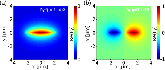
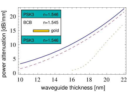
For proper design of the metallic stripe-waveguide, i.e., a quantitative prediction of the power attenuation as well as of the modal behavior, we first performed numerical simulations with a vectorial eigenmode solver [19]. The width of the gold-stripe (here 4.5 m) was chosen to give good end-fire coupling [20, 9] efficiency to a standard single-mode optical fiber. To avoid boundary effects like overlap of the computed plasmonic modes with the absorbing boundary of the simulation region we have chosen a m2 large area of the surrounding dielectric cladding. This choice of the simulation region guarantees that the computed power attenuation of each mode, i.e. the imaginary part of the effective refractive mode index, is only determined by the spatial overlap of the mode with the cross section of the lossy metal core. Fig. 1(a) and (b) show the simulated symmetric fundamental and anti-symmetric first-order LRSPP modes for a gold-stripe waveguide of 4.5 m width and 17 nm thickness embedded in the dielectric polymer benzocyclobutene (BCB) (refractive index: 1.545). Repeating such simulations for different gold film thicknesses and evaluating the imaginary part of the effective refractive index of each mode we obtain the desired power attenuation (see Fig. 2). As expected the attenuation decreases with decreasing gold-layer thickness, independent of the order of the mode. Additionally, because higher order modes are less localiced in the gold film, they experience a lower power loss than lower order modes.
To summarize our major design criteria, as a general rule of thumb, to minimize propagation loss of LRSPPs the gold film should be as thin as and the surrounding dielectric cladding as homogeneous as possible in terms of refractive index [7, 18, 9]. From an applied point of view (to avoid holes and islands during deposition of gold), however, the minimum propagation loss is limited by a minimum gold layer thicknessis of around 10 nm.
3 Fabrication
Gold-stripe waveguides are fabricated by first spin-coating a 13 m thick layer of BCB on a planar N-PSK3 glass substrate ( mm) from Schott. The BCB layer is baked softly in a drying oven (Memmert UM 100) at 100∘C and 209∘C for a time of 60 s and 40 min, respectively. The degree of polymerization of BCB after this soft bake is approximately 80 [21]. Onto that, nm thick gold stripes of m width are patterned via a lift-off technique. For that purpose, positive-tone photoresist Microposit S1813 is coated onto the sample, baked on a temperature stabilized hotplate, exposed with UV light, and developed in an alkaline developer Microposit 351 (diluted in water 1:3). The illumination is done with the help of a MJB3 mask aligner (Suess-MicroTec) using a 200 W mercury arc lamp. Gold is deposited with an electron beam evaporator (Telemark 271/277-32) which is part of an UHV chamber (BesTec). Subsequently, removing the photoresist in a bath of N-Methyl-2-pyrrolidone results in lifting off residual gold areas.
In contrast to standard photolithography in our case an adhesion promoter like Titanium can not be used for deposition of the gold layer due to disturbance of the refractive index of the sensitive layer structure needed for LRSPP propagation [7]. For that reason an additional layer below the photo resist – a so-called sacrificial layer of lift-off resist (LOR) – is used to create an undercut in the resist structure (see Fig. 3). This additional step is necessary to prevent the appearance of fence-like lift-off artifacts [21]. After lift-off the wafer is coated with a second 35 m thick layer of BCB which again is soft-baked at 100∘C for 60 s. This layer is then sealed with another planar glass substrate and finally the whole sample is cured in a nitrogen atmosphere at 233∘C for 120 min.
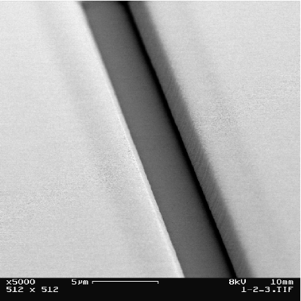
The quality of the gold stripes are inspected during the fabrication process, i.e. directly after lift-off. Here, a scanning electron microscope (Zeiss LEO DSM 982) is used for an overview of defects whereas the stripe width and height are determined with an atomic force microscope (AFM). To avoid systematic errors in AFM height measurements on different substrate materials (here gold and BCB) spare samples from the same fabrication run are coated prior to inspection with a thin layer of gold [21, 22]. In addition the thickness of the gold-stripe waveguide is cross-checked independently from the AFM measurement with an oscillating crystal installed in the electron beam evaporation chamber. Typical errors in the determination of the height are on the order of nm. For further optical characterization the samples are first cut with a diamond wire saw to different lengths (here 1 and 2 mm). Finally, the sample and the waveguide facets are carefully polished with silicon carbide and aluminum oxide fiber lapping sheets (minimum grain size m).
4 Optical characterization
To characterize the power attenuation of the LRSPP we analyze the damping of butt-coupled light (see Fig. 4(a)). In detail, a laser beam at a wavelength of 780 nm is coupled into a polarization maintaining optical single mode fiber. For optimum end-fire coupling to the LRSPP the cleaved end facet of the optical fiber is precisely positioned with piezo-controlled mechanical XYZ-translation stages with respect to the optical axis of the plasmonic waveguide. To optimize coupling to the -polarized LRSPP modes [7] the exciting laser polarization is aligned parallel to the y-axis, i.e. perpendicular to the gold layer. For a measured gold stripe width of m and thickness of nm we numerically estimate propagation loss of dB/mm and a maximum end-fire coupling efficiency of 69 for the fundamental LRSPP mode. Light transmitted by the waveguide is imaged in propagation direction of the LRSPP onto a calibrated CCD camera (see Fig. 4), for detailed analysis of the mode structure.
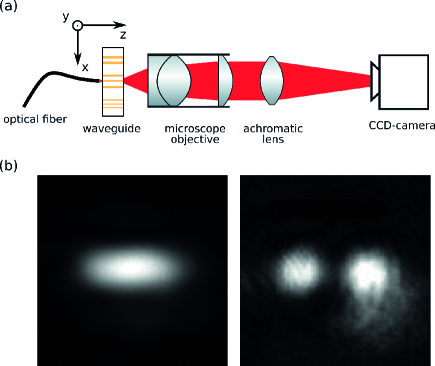
For a fabricated waveguide of m width we observe either the symmetric fundamental mode or a superposition with the anti-symmetric first-order LRSPP mode. When the symmetric mode of the butt-coupling fiber is centered laterally with respect to the waveguide, only the symmetric fundamental LRSPP mode is excited (see Fig. 1(b)). For a small lateral displacement (less than the mode field diameter) of the optical fiber with respect to the plasmonic gold-stripe both the fundamental and first-order LRSPP modes are excited, yet with different excitation amplitudes. Because these modes exhibit different effective refractive indices (1.553 and 1.549 at nm for the fundamental and first-order mode, respectively) they pick up different phases during propagation and at the end of the waveguide both modes add up coherently, resulting in a multi-mode interference pattern [23, 24]. As such interference pattern depends sensitively on the ratio of amplitudes and the phase between both LRSPP modes, experimental analysis of the modal behaviour of our LRSPP waveguides has to take this into account. E.g., for a large lateral displacement of the butt-coupling fiber the anti-symmetric first-order LRSPP mode is excited better than the symmetric fundamental mode. In this case at the output of the waveguide we observe a multi-mode interference pattern which is dominated by the anti-symmetric first order mode. As the fundamental LRSPP mode is always excited this leads to an asymmetry in brightness between the right and left spot of the observed interference pattern (see Fig. 4(b), right). To clearly demonstrate that the observed modes are of plasmonic nature the polarization of the exciting laser is rotated by 90 degrees (parallel to the x-axis). As expected from our numerical simulations of the polarization properties of the LRSPP modes the observed modes disappear (exctinction ratio 1:100) because they can not be excited.
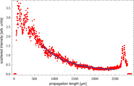
To get a representative value of the mode power attenuation we investigate 8 equivalent waveguides on one fabricated chip. Step-by-step we couple laser light via the butt-coupling fiber to one of the waveguides and optimize the coupling to the fundamental mode by monitoring the shape of the outcoupled LRSPP mode at the polished facet of the chip. To determine the mode power attenuation (propagation damping) of the fundamental LRSPP mode, we measure with a second calibrated CCD camera (not shown in Fig. 4) the decrease of scattered light in top-view configuration (optical imaging axis parallel to the y-axis). As the imaged width of a waveguide spreads over several pixel of the CCD camera, we integrate the measured intensity of the scattered light over 64 pixel in a line perpendicular to a waveguide. For each of the 8 waveguides on the chip we than fit the decrease of scattered light in a line parallel to the waveguide with an exponential function (see Fig. 5). To get an accurate propagation damping we on purpose skip the in- and out-coupling sections of the waveguides, where e.g. uncoupled light from the optical fiber leaks into the sandwitched layer structure of our chip (see e.g. inset of Fig. 2). Averaging over the fit results of all eight examined waveguides we finally determine a propagation loss of dB/mm. Within our measurement error this finding is in good agreement with the calculated propagation loss of dB/mm.
5 Summary and outlook
In summary, we demonstrated the excitation and long-range propagation of a SPP along a planar gold-stripe waveguide at an optical wavelength of 780 nm. For a stripe width of 4.5 m and height of nm we measured a propagation damping of dB/mm. This achievement together with the possibility to embed e.g. narrowband solid state quantum emitters like SiV centers hosted in diamond nano-crystals [16] in the BCB cladding layer [13, 25] forms an ideal basis for future efficient coupling of single-emitter resonance fluorescence to LRSPP waveguides.
Acknowledgments
We acknowledge funding from the DFG through the excellence cluster NIM and the Forschergruppe 1493. TT acknowledges support from the Japanese Society for the Promotion of Science.
References
References
- [1] H. Ditlbacher et al., Optics Express 16, 10455 (2008).
- [2] R. W. Heeres, L. P. Kouwenhoven, and V. Zwiller, Nature Nanotechnology 8, 719 (2013).
- [3] J. R. Lakowicz et al., Analyst 133, 1308 (2008).
- [4] A. W. Schell, G. Kewes, T. Hanke, A. Leitenstorfer, R. Bratschitsch, O. Benson, and T. Aichele, Opt. Express 19, 7914 (2011).
- [5] A. V. Akimov et al., Nature 450, 402 (2007).
- [6] R. Kolosev et al., Nature Phys. 5, 470 (2009).
- [7] P. Berini, Phys. Rev. B 61, 10484 (2000).
- [8] R. Charbonneau, P. Berini, E. Berolo, and E. Lisicka-Shrzek, Opt. Lett. 25, 844 (2000).
- [9] P. Berini, Advances in Optics and Photonics 1, 484 (2009).
- [10] E. Altewischer, M. P. Exter, and J. P. Woerdman, Nature 418, 304 (2002).
- [11] S. Fasel et al., Phys. Rev. Lett. 94, 110501 (2005).
- [12] A. Huck et al., Phys. Rev. Lett. 102, 246802 (2009).
- [13] M. C. Gather, K. Meerholz, N. Danz, and K. Leosson, Nature Photonics 4, 457 (2010).
- [14] Z. Jacob and V. M. Shalaev, Science 334, 463 (2011).
- [15] C. Wang, C. Kurtsiefer, H. Weinfurter, and B. Burchard, J. Phys. B 39, 37 (2006).
- [16] E. Neu, C. Arend, E. Gross, F. Guldner, C. Hepp, D. Steinmetz, E. Zscherpel, S. Ghodbane, H. Sternschulte, D. Steinmueller-Nethl, Y. Liang, A. Krueger, and C. Becher, Appl. Phys. Lett. 98, 243107 (2011).
- [17] I. De Leon and P. Berini, Phys. Rev. B 78, 161401(R) (2008).
- [18] T. Nikolajsen, K. Leosson, I. Salakhutdinov, S. I. Bozhevolnyi, Appl. Phys. Lett. 82, 668 (2003).
- [19] Z. Zhu and T. G. Brown, Opt. Express 10, 853 (2002).
- [20] G. I. Stegeman, R. F. Wallis, and A. A. Maradudin, Opt. Lett. 8, 386 (1983).
- [21] J. Trapp, Diploma Thesis, Technical University Munich (2011).
- [22] G. Bar, R. Brandsch, and H.-J. Cantow, Langmuir 13, 3807 (1997).
- [23] R. Zia, J. A. Schuller, and M. L. Brongersma, Phys. Rev. B 74, 165415 (2006).
- [24] Y. L. Lee, Opt. Express 17, 10718 (2009).
- [25] A. Schell et al., Scientific Reports 3, 1577 (2013).