Phase Cascade Bridge Rectifier Array in a 2-D lattice
Abstract
We report on a novel rectification phenomenon in a 2-D lattice network consisting of sites with diode and AC source elements with controllable phases. A phase cascade configuration is described in which the current ripple in a load resistor goes to zero in the large limit, enhancing the rectification efficiency without requiring any external capacitor or inductor based filters. The integrated modular configuration is qualitatively different from conventional rectenna arrays in which the source, rectifier and filter systems are physically disjoint. Exact analytical results derived using idealized diodes are compared to a realistic simulation of commercially available diodes. Our results on nonlinear networks of source-rectifier arrays are potentially of interest to a fast evolving field of distributed power networks.
I Introduction
The need for DC electrical power generation from AC sources is arguably the most important nonlinear problem in modern society. Interest in distributed energy networksBlaabjerg2006 , alternative energy technologies Dresselhaus2001 ; Mateen2016 and the need for energy harvestingAlavikia2015 and energy scavenging Qin2008 systems has spurred renewed interest in the problem. A very large number of configurations have been investigated for power generation from AC source networks, and extend to wireless power generation Popovic2013 ; Alavikia2015 , rectenna arraysOlgun2011 ; Hagerty2004 and smart gridsFarhangi2010 . Of particular interest is the generation of DC power, not only for its ubiquiitous use but also for efficiency in transmission over long distances with asynchronous power generators with a wide range of sources for energy harvesting. A classic configuration consists of a rectennaBrown1984 in which diode arrays are used to rectify the output of a receiving antenna, followed by filters to provided the desired DC power. Such nonlinear networks have become very interesting recently in models in which diode elements are integrated into plasmonic structures, in the rapidly emerging new field of nonlinear metamaterialsPoutrina2010 ; Lapine2014 , among others. The ability to design and engineer local phase shifts within each element of a receiving array represents a new capability that has not been studied at all, and possible configurations remain underexplored. Lattice networks consisting of nonlinear elements like diodes have been extensively studied in statistical physics, in directed networks and percolation problemsredner:1982 , and random circuit element networksKarpov2003 ; Dearcangelis1985 ; Derrida1982 . The range of phenomena is potentially vast even for deterministic systems. Up to now, the inclusion of voltage sources within the lattice sites has not been considered. It may be expected that integration of sources with random or varying phases at each lattice site will lead to an even richer range of phenomena. Distributed generation of power from both conventional and alternative energy sources provides motivation to study networks in which voltage sources are also distributed throughout the lattice.
In this article, we investigate rectification phenomena in a particular 2-D lattice network consisting of sites in which each lattice site consists of an AC source in a bridge-rectifier like configuration. Each lattice site shares one diode with each of its nearest neighbors, as shown in Figure 1. The configuration is inspired by rectenna arrays, but now with the addition of AC sources at each lattice site. The system consists of AC sources, and diodes. It can be seen that when , the configuration is identical to a classic Bridge rectifier combination. The current through the load resistor has many frequency components, with the zero frequency DC component being the most important for rectification. Our results show that an exact analytical result valid for arbitrarily large can be derived even for such a strongly nonlinear system with idealized diodes.
II Models
We consider how to arrange a lattice of AC voltage sources, with suitably chosen relative phases and with diodes for rectification, to produce an almost dc source. For definiteness, consider a 2-D lattice of elements arranged as shown on the right side of Figure 1. In the next section, we present the analysis for idealized diodes, which operate in just two states determined by the bias voltage across the diode: (i) an “off’ state, at negative bias, where the current is zero; (ii) an “on” state, at positive bias, where the current is an arbitrary positive value limited only by the load. In the following section, the results are compared to the results of simulations using commercially available Silicon diodes with a forward bias set by the bandgap of Silicon, and current set by a non-zero forward resistance.

For comparison, we extend the series arrangement shown on the left side of Figure 1 to the case where voltage sources are arranged in series with a load resistor . The total number of diodes required is . Each diode must then be rated to carry up to the maximum total current flowing through the load resistor, which limits the utility of the series configuration. The phases of the voltage sources are uniformly distributed between zero and With the rectified sources in series, the total voltage at time is
| (1) |
Clearly, this is a periodic function of time, with time period For the simple case when is an even number, we have
| (2) |
are the minima and maxima of
The ratio of minimum to maximum voltage is and the frequency of these ripples is For large the ripples have height and are superimposed on a dc voltage of We note that the peak current carried through each diode is approximately , which it carries for half the cycle. For large this current can exceed the maximum rating for the diode in the series configuration.
The current load in each diode can be reduced by adopting a parallel configuration (see the left side of Figure 1 ). For bridge rectifiers arranged in a parallel configuration, the sources have to be in phase. The fraction of the ripple in the output voltage can be seen to be just as large it would for a single rectifier, and additional filtering would be needed to get DC current through the load resistor.
These elementary statements motivate us to investigate a hybrid system that combines series and parallel combinations into the 2D lattice shown in Figure 1, with each unit cell is mapped onto a conventional bridge rectifier. Remarkably, we find that for a special choice of phases of the AC sources, the configuration provides the advantage of reduced ripple in the rectified DC voltage of a series combination, with the advantage of reduction in peak current that is the hallmark of the parallel combination.
III Analytical results
In this alternative arrangement shown on the right side of Figure 1, diodes are placed on the vertical sides of the square, and voltage sources on the horizontal sides. Conducting strips at the top and the bottom are linked to the external load. The voltage across the source in the ’th row and ’th column is
| (3) |
where and The sign of the voltage across a source is fixed by defining it as the difference between the voltage at the right end and at the left end of the source. Then one can verify that the voltage at the ’th junction between voltage sources in the ’th row is
| (4) |
where and is a -independent function of time in the ’th row that has to be determined. (Eq.(4) can be verified by taking the difference in the voltages at successive nodes and comparing to Eq.(3).) The voltages are then the voltages at the ends of the various diodes. The functions can be determined by the conditions that, for idealized diodes, i) the voltage across each diode must be negative or zero ii) at least one diode per row must have a non-negative voltage across it so that current can flow from the row of voltage sources above it to the row below. This ensures that
| (5) |
indepdent of for This fixes Similar reasoning can determine the voltages at the conducting strips at the top and bottom of the lattice.
To understand the results obtained, we first consider a continuum approximation, where the number of nodes in each row is very large. From Eq.(4), the voltage across any row is a sinusoidal curve with amplitude The sinusoidal curve for each row is upside down compared to the adjacent rows. (The curve in each row is also shifted horizontally by a phase of with respect to the preceding row, but this shift is neglegible in the limit.) From Eq.(5), we immediately obtain
| (6) |
where Thus By the same reasoning, the voltages of the two conducting strips are and Therefore the voltage difference between the two conducting strips is and a DC current flows across the load resistor.
With an understanding of the behavior of the ideal phase cascade shown in the limit, we now consider the case of a finite lattice, with an even number for simplicity. The displacement in the sinusoidal curves for successive rows, i.e. is obtained by the condition
| (7) |
Because is even, replacing changes the sign of both cosine terms. Since the minimum over all is taken, the factor of can be dropped. We can also replace the minimum with the maximum, with a change of sign, with :
| (8) |
The voltage of the conducting strip at the top of Figure 1 is
| (9) |
where we have used the fact that reverses the function. The voltage of the conducting strip at the bottom of Figure 1 is similarly
| (10) |
where we have replaced with to absorb a phase of from The voltage difference between the two conducting strips can be obtained by subtracting these two equations. It is convenient to write this as
| (11) |
by formally extending Eq.(7) to with where
| (12) | |||||
For the first part of Eq.(11), using Eq.(8),
| (13) |
where we define and we have used the periodicity of the summand with respect to to change the limits of the sum. This is a periodic function of time, with a period of If which covers one time period, every term in the sum on the right hand side of Eq.(13) is maximized at Thus the minima and maxima of occur at
| (14) |
and
| (15) |
The ratio of the two is Thus for large tends a dc voltage of magnitude with ripples whose frequency is and height is
We now turn to From Eq.(12), is periodic with a period Furthermore, unless the two cosine functions have their maxima at different values of The first cosine has its maximum at for while the second cosine has its maximum at for Thus is non-zero within the narrow time interval or more generally, for integer The maxima of occur when It is easy to evaluate Eq.(12) at and verify that
| (16) |
Combining with the result of the previous paragraph, has a ripple of height and frequency and a ripple of height and frequency superimposed on the dc voltage
We now compare the square lattice with voltage sources to full-wave rectifiers in series. For a distributed voltage source, it is reasonable to choose the amplitude of the individual sources to scale as i.e. Then, the DC voltage for the square lattice is compared to for the rectifiers in series. On the other hand, for large there is only one diode per source instead of four. As mentioned earlier, for a load the maximum current flowing through each diode is for the series configuration. Similarly, for the square lattice with idealized diodes, the maximum current is because at any instant the current flows from top to bottom along a unique set of diodes. However, with realistic diodes, the current is distributed over numerous parallel ‘channels’, reducing the maximum current. (Without numerical simulations, it is not obvious whether the number of channels is or ) Thus for the same current flowing through the load resistor, it is easier to exceed the maximum rating of the diodes for rectifiers in series. The maximum voltage across a diode when it is reverse biased is for the rectifiers in series. For the lattice, the maximum reverse biased voltage can be approximately obtained from the continuum approximation, as Both of these are well behaved for large Finally, the power dissipated in the diodes is non-zero if they are not ideal. Since
| (17) | |||||
the instantaneous power dissipated is
| (18) |
where the sums run over the forward and reverse biased diodes respectively. For the lattice, there are reverse biased diodes with voltages across them, and the power dissipated in them is For the forward biased diodes, if the current flows along channels, there are forward biased diodes each with a current flowing through it. The power dissipated in the forward biased diodes is thus By comparison, for the rectifiers in series, there is an current flowing in forward biased diodes, so that the power dissipated in them is
Our results show prefect rectification can be achieved using a nonlinear network consisting of a lattice of AC sources. This work provides an interesting example of an exact result that can be established for an infinite nonlinear network, consisting of ideal bridge rectifiers that are of interest for distributed energy generation. In the next section, simulations with realistic diodes confirm the exact results derived here. Importantly, the phase cascade sequence described is independent of frequency, and perfect rectification can be achieved for a wide range of frequencies, which makes it attractive for energy harvesting and distributed energy networks.
IV Numerical simulations
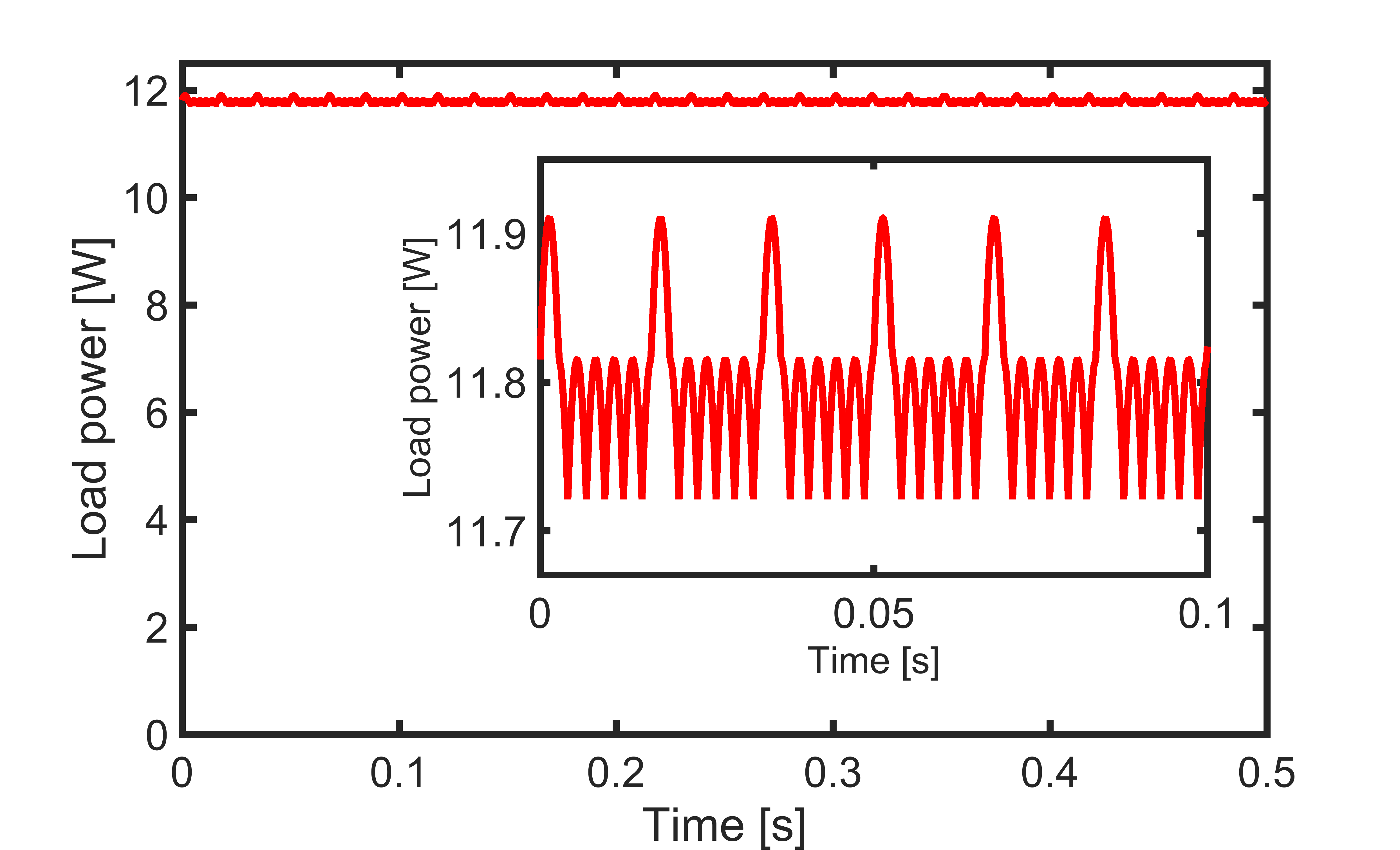
Simulations were performed in MATLAB Simulink, using Silicon diodes, with model parameters selected for a General purpose Rectifier Fairchild 1N4004). The amplitude of the AC sources was set at 10 V, and the frequency was set to 10Hz, driving a load a 1 k load resistor. Current probes were used to measure the load current, and the current and voltage difference across selected diodes and AC power sources. The load current was used to derive the load power. Shown in Figure 2 are the results of the simulation of the power for the 2-D square lattice with the Phase Cascade Array.
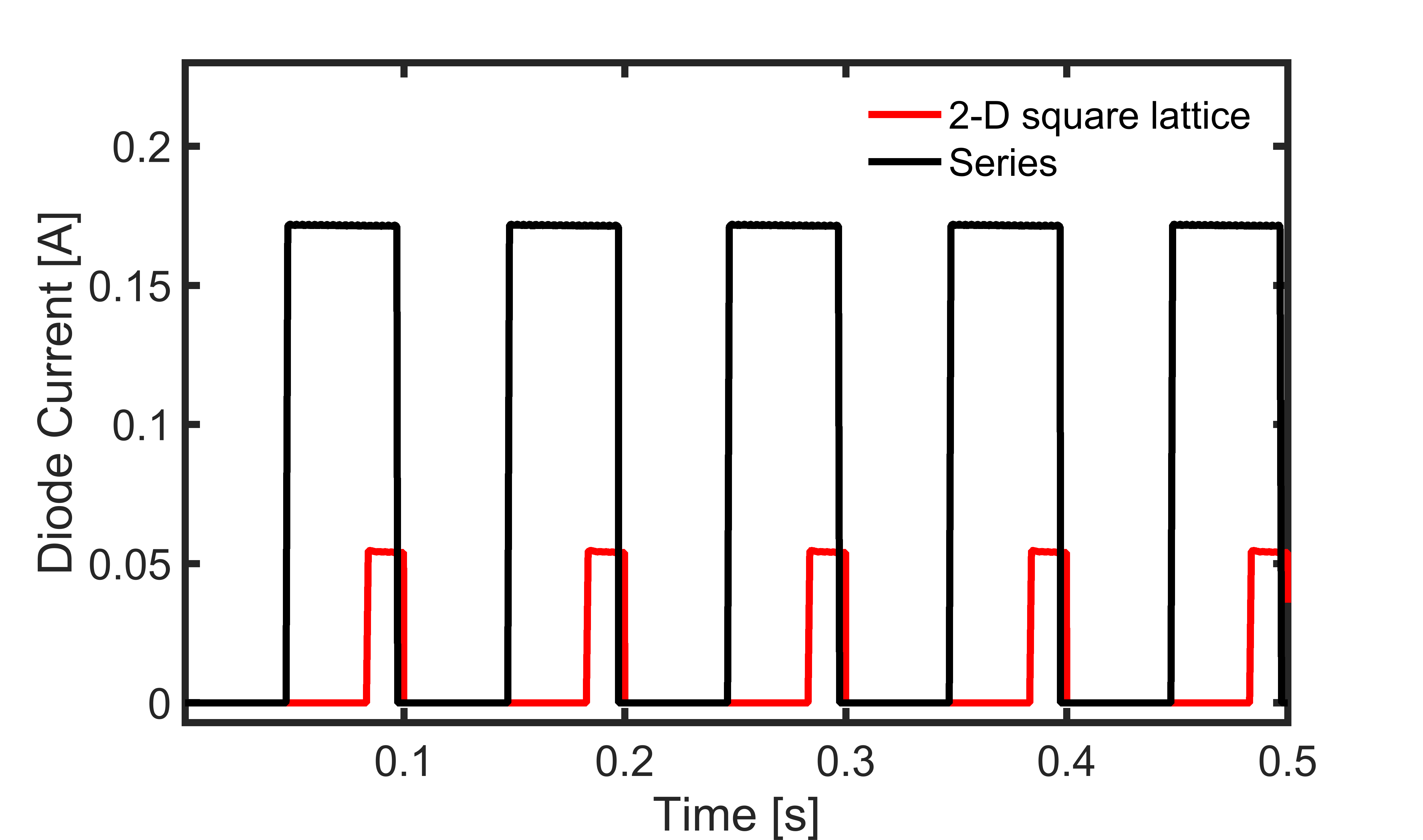
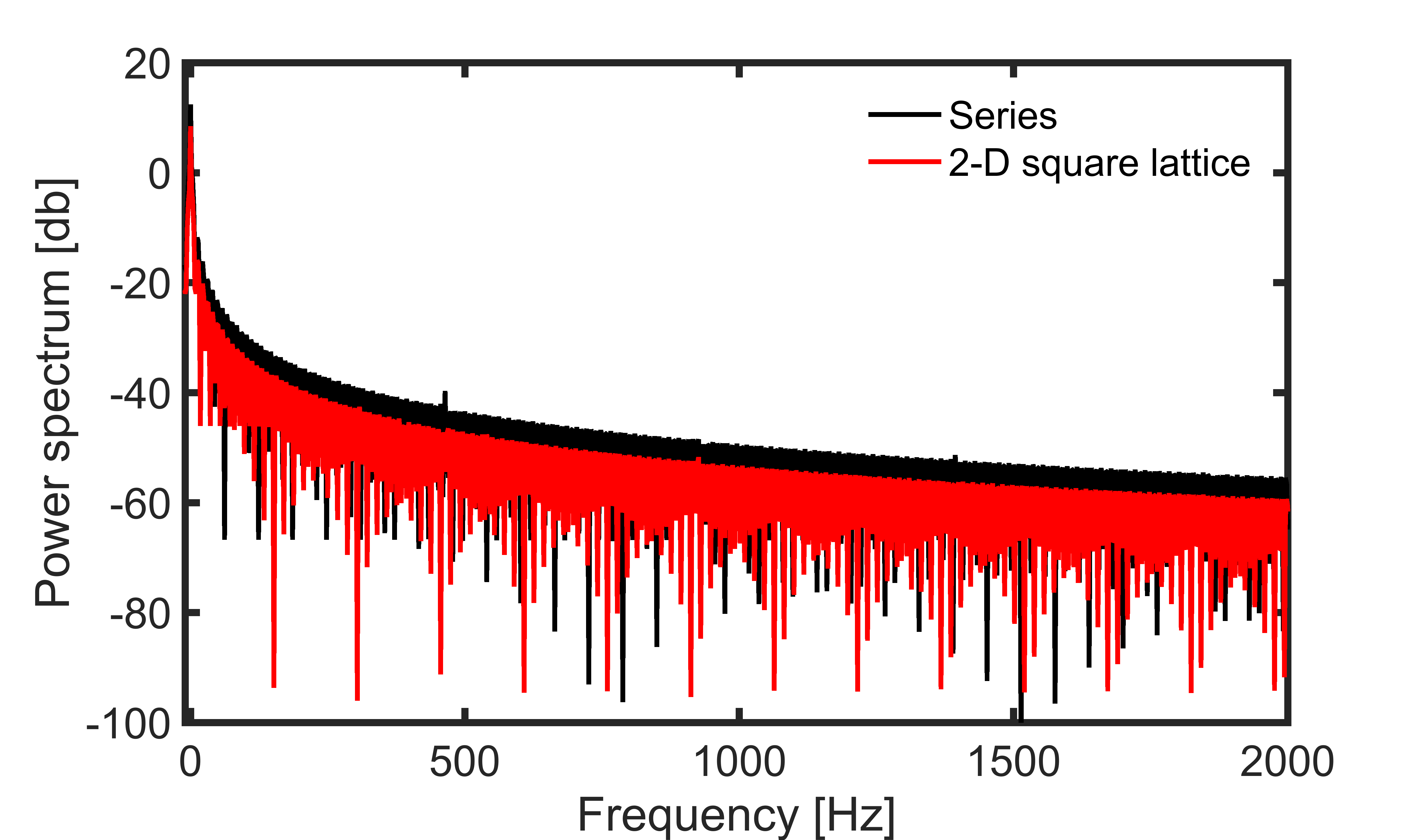
The simulations were used to calculate the representative duty cycle of the Phase Cascade Array, compared to the series configuration in Figure 3. It is evident that in the Phase Cascade Array, the peak current is lower, and the duty cycle also lower than in the Series configuration, reducing both thermal load and easing the limits on the forward current. Fast Fourier Transforms of the time series were used to calculate the power spectrum in the load resistor. Figure 4 shows a comparison of the power spectrum for the Phase Cascade Array compared to the series configuration.
V Acknowledgements
Acknowledgements.
M. Nazari acknowledges support from a Graduate Fellowship in the ECE department at Boston University. We thank C. Maedler, R. Averitt, and members of the Photonics Center staff for assistance.References
- (1) F. Blaabjerg and R. Teodorescu and M. Liserre and A. V. Timbus “Overview of Control and Grid Synchronization for Distributed Power Generation Systems” IEEE Transactions on Industrial Electronics, 53: 1398-1409 (2006).
- (2) M. S. Dresselhaus, I. L. Thomas “Alternative energy technologies” Nature 414: 332-337 (2001).
- (3) F. Mateen, C. Maedler, S. Erramilli, P. Mohanty “Wireless actuation of micromechanical resonators” Microsystems & Nanoengineering 2: 16036 (2016).
- (4) Z. Popovic “Cut the Cord” IEEE Microwave Magazine 14:55-62 (2013).
- (5) B. Alavikia, T. S. Almoneef, O. M. Ramahi “Wideband resonator arrays for electromagnetic energy harvesting and wireless power transfer” Applied Physics Letters 107: 243902 (2015).
- (6) Y. Qin, X.D. Wang, Z. L. Wang “Microfibre-nanowire hybrid structure for energy scavenging” Nature 451: 809 (2008).
- (7) U. Olgun, C.C. Chen, J. L. Volakis “Investigation of Rectenna Array Configurations for Enhanced RF Power Harvesting” 10: 262-265 (2011).
- (8) J. A. Hagerty, F. B. Helmbrecht, W. H. McCalpin, R. Zane, Z. B. Popovic IEEE Transactions on Microwave Theory and Techniques 52:1014 (2004).
- (9) H. Farhangi, “The Path of the Smart Grid”, IEEE Power and Energy January/February issue pp 19-28 (2010) doi: 10.1109/MPE.2009.93486
- (10) W. C. Brown, “The history of power transmission by radio waves” IEEE Trans. MTT 32L 1230-1242 (1984).
- (11) E. Poutrina, D. Huang, D. R. Smith “Analysis of nonlinear electromagnetic metamaterials”, New Journal of Physics 12 093010 (2010).
- (12) M. Lapine, I. V. Sandrivov, Y. S. Kivshar “Colloquium: Nonlinear Metamaterials”, Rev Mod Physi 86: 1093 (2014).
- (13) S. Redner, “Directed and diode percolation”, Phys Rev B 25, 3242-3250 (1982).
- (14) V. G. Karpov “Critical Disorder and Phase Transitions in Random Diode Arrays” Phys. Rev. Lett. 91:226806 (2003).
- (15) L. Dearcangelis, S. Redner, A. Coniglio “Anomalous Voltage Distribution of Random Resistor Networks and a New Model for the Backbone at the Percolation-threshold” Phys. Rev B 31:4725-4727 (1985).
- (16) B. Derrida, J. Vannimenus “A Transfer-Matrix Approach to Random Resistor Networks” J Phys. A - Mathematical and General 15:L557-L564 (1982).