Method for Transferring High-Mobility CVD-Grown Graphene with Perfluoropolymers
Abstract
The transfer of graphene grown by chemical vapor deposition (CVD) using amorphous polymers represents a widely implemented method for graphene-based electronic device fabrication. However, the most commonly used polymer, poly(methyl methacrylate) (PMMA), leaves a residue on the graphene that limits the mobility. Here we report a method for graphene transfer and patterning that employs a perfluoropolymer—Hyflon—as a transfer handle and to protect graphene against contamination from photoresists or other polymers. CVD-grown graphene transferred this way onto LaAlO3/SrTiO3 heterostructures is atomically clean, with high mobility (~30,000 cm2V-1s-1) near the Dirac point at 2 K and clear, quantized Hall and magneto-resistance. Local control of the LaAlO3/SrTiO3 interfacial metal-insulator transition—through the graphene—is preserved with this transfer method. The use of perfluoropolymers such as Hyflon with CVD-grown graphene and other 2D materials can readily be implemented with other polymers or photoresists.
Single-layer graphene has proven to be an extraordinary 2D material system due to its unique properties such as a high mobility 2D electron gas and Dirac behavior of electronsNovoselov et al. (2004, 2005); Geim and Novoselov (2007); Geim (2009). A key factor influencing the high mobility of graphene-based electronic devices is the method for fabricating and transferring graphene onto a given substrate. Current state-of-the-art high-mobility graphene devices are created from mechanical exfoliation followed by encapsulation with hexagonal boron nitride (h-BN)Dean et al. (2010). For applications requiring an arbitrary substrate and graphene shape, CVD growth followed by transfer of graphene on a PMMA scaffold is preferred Li et al. (2009); Reina et al. (2008, 2009). However, residual PMMA remaining after graphene transfer is known to be a source of electron scattering, significantly limiting the graphene mobilityPirkle et al. (2011); Lin et al. (2012); Cheng et al. (2011). Annealing in H2/Ar environment can partially remove the PMMA residue, but this process can introduce structural defectsLin et al. (2012) or greatly increase coupling to the substrate, resulting in extrinsic doping and even deterioration of mobilityCheng et al. (2011).
We have developed a graphene transfer method that incorporates an amorphous perfluoropolymer, HyflonTM AD 60 (Solvay), to physically separate a hard-to-remove polymer from the graphene. Hyflon has been widely used in membrane applications such as fuel cellsArcella, Troglia, and Ghielmi (2005); Merlo et al. (2007); Zhang et al. (2012) due to the chemical inertness of C-F bond and high selectivity to solvents, such as FluorinertTM FC-40. Recently, it has been reported that inserting a Hyflon membrane between graphene and a hydrophilic substrate like SiO2 can reduce the extrinsic p-type doping in graphene by preventing water vapor adsorption to the dangling bonds on the substrateMattevi et al. (2012).
The substrate we chose is a heterostructure consisting of bulk TiO2-terminated SrTiO3 (STO) with a thin layer of LaAlO3 (LAO) on top. The LAO is grown with pulsed laser deposition using methods described elsewhereHuang et al. (2015). The LAO/STO system is known for the formation of a 2D electron gas (2DEG) at the interface when the thickness of LAO is larger than a 4 unit cell critical thicknessOhtomo and Hwang (2004); Thiel et al. (2006). Many other interesting properties have been reported on the LAO/STO interface as well, such as magnetism Brinkman et al. (2007); Li et al. (2011); Bi et al. (2014), superconductivityReyren et al. (2007), and electron pairing without superconductivityCheng et al. (2015). For the LAO/STO samples with a critical thickness (3.4 unit cells) the interface is nominally insulating; however, an insulator-to-metal transition can be achieved by scanning the surface with a positively biased conductive atomic force microscope (c-AFM) tipCen et al. (2008, 2009). The graphene/LAO/STO system has been investigated previously using mechanically exfoliated graphene; it was found that c-AFM writing of LAO/STO nanostructures can be performed in the presence of a graphene top layerHuang et al. (2015). We have fabricated graphene/LAO/STO heterostructure with CVD-grown graphene and and transferred using a PMMA scaffoldJnawali et al. (2016), but the residue of PMMA on LAO and graphene was difficult to remove.
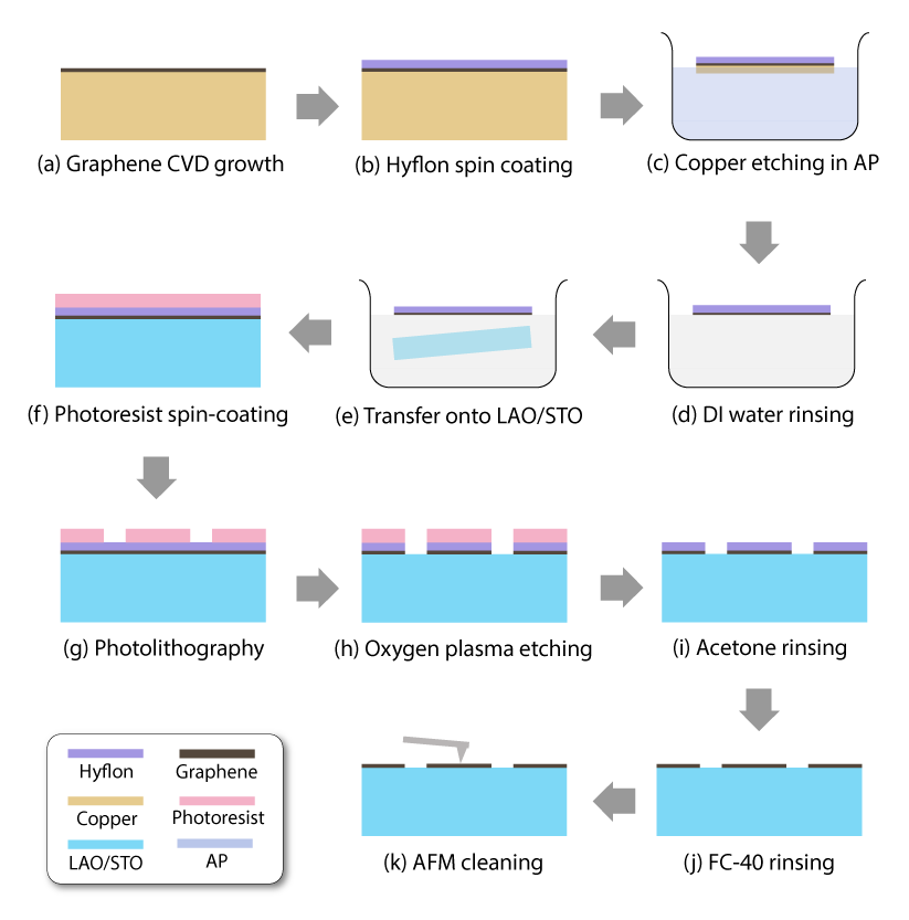
The sample preparation procedures are illustrated in FIG. 1. Graphene is grown on ultra-flat diamond turned copper substrates using atmospheric pressure chemical vapor deposition (APCVD)Dhingra et al. (2014) (FIG. 1(a)). The size of single crystal graphene domains can reach 70 . 0.5% Hyflon FC-40 solution is spin-coated and baked on a 95 ∘C hotplate for 1 minute (FIG. 1(b)). The typical Hyflon thickness is 80 nm. The Hyflon-coated graphene/Cu is placed on the surface of 1 mol/L ammonium persulfate (AP) solution for 3 hours until the copper is completely dissolved (FIG. 1(c)), and then the Hyflon with graphene is captured and rinsed in DI water three times (FIG. 1(d)). The Hyflon with graphene is left floating on the water surface. An LAO/STO substrate with pre-patterned electrodes is immersed underneath the graphene and then lifted to the water surface so that the Hyflon with graphene rests atop the LAO/STO surface (FIG. 1(e)). The LAO/STO with Hyflon and graphene is baked at 50 ∘C in an oven for 3 minutes. AZ4210 photoresist is spin-coated onto the Hyflon (FIG. 1(f)) and patterned with 365 nm UV exposure (FIG. 1(g)). The Hyflon and graphene in the patterned region is etched by oxygen plasma (FIG. 1(h)). The undeveloped photoresist is removed with acetone and isopropanol (IPA) (FIG. 1(i)), leaving only Hyflon on the patterned graphene. The sample is placed into hot FC-40 liquid (180 ∘C), and then shaken for 48 hours while the liquid cools slowly to room temperature (FIG. 1(j)). Finally, the residual Hyflon is cleared by AFM scanning.
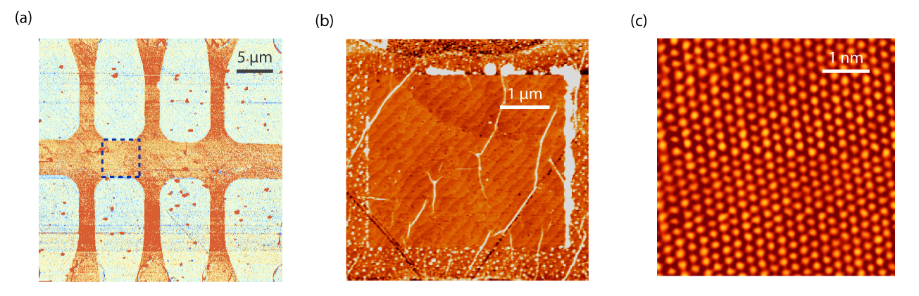
Patterned graphene is distinguishable from bare LAO on the phase channel image from AFM AC mode scan (FIG. 2(a)). Hyflon residue is still visible on the graphene right after Hyflon removal with FC-40, with a typical thickness of 1 nm. Larger particles of several hundreds of nanometers size from the FC-40 are scattered over the entire sample. The thin layer of Hyflon and larger particles can be moved around on the surface using contact-mode AFM scanning (FIG. 2(b)). Within the contact scan area, 4 Å unit-cell steps of LAO are distinguishable, in addition to some wrinkles on the graphene. Residue from the Hyflon accumulates at the perimeter of the contact-scanned area. In some places where the graphene has fractured due to prior contact-mode AFM scanning, the graphene can peel from the LAO surface (not shown in the figure). Generally, contact-mode AFM scanning leaves the graphene surface atomically flat and clean. FIG. 2(c) shows a room-temperature STM image of the graphene/LAO/STO surface after AFM cleaning has been performed.
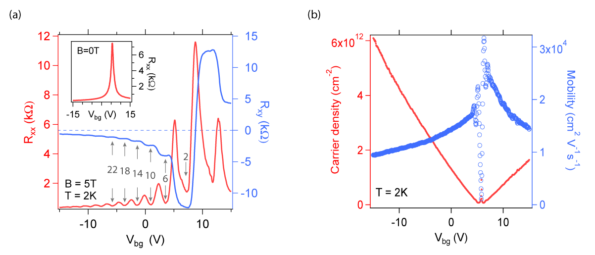
The low-temperature () graphene mobility increases two-fold after cleaning, consistent with other reportsGoossens et al. (2012); Lindvall, Kalabukhov, and Yurgens (2012). At 2 K, the Dirac point was at +7 V (FIG. 3(a) inset) meaning that the ungated graphene is slightly p-type doped on LAO/STO. Away from the Dirac point the mobility is about 10,000 cm2V-1s-1 (FIG. 3(b)), while it reaches 30,000 cm2V-1s-1 close to the Dirac point, which is higher than most of the wet transferred CVD graphene reported. The hole carrier density reaches 61012 cm-2 at a backgate voltage of only -15 V, owing to the high dielectric constant of STO at low temperaturesWeaver (1959). On the electron side however, the carrier density does not exceed 1.5 cm-2 (not shown in the figure), likely due to the formation of a 2D electric gas between the sub-critical thickness LAO and STO at positive backgatesThiel et al. (2006) and subsequent screening of the electric field. When a 5 tesla magnetic field is applied at 2 K, clear quantization of magnetoresistance and Hall resistance is observed as a function of backgate voltage. The filling factor of the quantum Hall states satisfy the known single-layer graphene quantization condition , as indicated in FIG. 3(a).
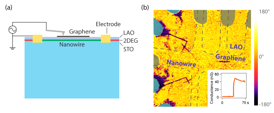
It has previously been demonstrated that conductive nanostructures can be “written” at the LAO/STO in the presence of exfoliated grapheneHuang et al. (2015). Here we investigate whether this property is preserved for CVD-grown graphene transferred with the Hyflon-based procedure described above. FIG. 4(a) illustrates the configuration under which conductive nanostructures are created and probed. The inset of FIG. 4(b) shows the characteristic current jump that results when a conductive nanostructure is created between two interfacial electrodes. Typical conductance of a nanowire underneath the graphene area is about 50 nS. In this case, the path of the current lies underneath the graphene Hall bar channel. Piezoforce microscopy (PFM) is employed as a method for determining the local carrier density underneath the graphene. This technique has been previously established for LAO/STO, where it was found that the carrier density is proportional to the piezoelectric response (up to a constant offset)Huang et al. (2013). FIG. 4(b) shows the nanowire (deep purple areas) written underneath and outside the graphene (enclosed by dashed gray lines). Electrodes connected to the interface and graphene are painted with blue and grey color respectively. Several nanowire writings were attempted before the PFM imaging, therefore some other high carrier density features are visible. The nanowire under the graphene has a slightly smaller piezoelectric response due to electrical shielding by the graphene, causing the contrast to be diminished somewhat.
In summary, we have developed a robust method for successful transfer of graphene onto the surface of LaAlO3/SrTiO3 using Hyflon. Mobility of the graphene could reach 10,000 to 30,000 cm2V-1s-1 at 2 K, which is higher than most reports of CVD-grown graphene after wet transfer and patterning with PMMA. Clear quantization of magnetoresistance and Hall resistance plateaus is observed. The method of using Hyflon as a buffer layer against other photoresists or polymer may find more widespread use in the growing field of two-dimensional materials that are synthesized by means other than mechanical exfoliation. For the specific case of graphene/LAO/STO, the combination of high mobility with the capability of locally controlling the electron density at the LAO/STO interface opens new avenues for interesting and potentially fruitful interactions between these two intimately coupled electronic systems.
Support for this research by ONR (N00014-13-1-0806), AFOSR (FA9550-10-1-0524), NSF (DMR-1124131), AFOSR (FA9550-15-1-0334) and AOARD (FA2386-15-1-4046) is gratefully acknowledged.
References
- Novoselov et al. (2004) K. Novoselov, A. Geim, S. Morozov, D. Jiang, Y. Zhang, S. Dubonos, I. Grigorieva, and A. Firsov, Science 306, 666 (2004).
- Novoselov et al. (2005) K. Novoselov, A. Geim, S. Morozov, D. Jiang, M. Katsnelson, I. Grigorieva, S. Dubonos, and A. Firsov, Nature 438, 197 (2005).
- Geim and Novoselov (2007) A. Geim and K. Novoselov, Nature Materials 6, 183 (2007).
- Geim (2009) A. Geim, Science 324, 1530 (2009).
- Dean et al. (2010) C. Dean, A. Young, I. Meric, C. Lee, L. Wang, S. Sorgenfrei, K. Watanabe, T. Taniguchi, P. Kim, K. Shepard, and J. Hone, Nature Nanotechnology 5, 722 (2010).
- Li et al. (2009) X. Li, Y. Zhu, W. Cai, M. Borysiak, B. Han, D. Chen, R. D. Piner, L. Colombo, and R. S. Ruoff, Nano Letters 9, 4359 (2009).
- Reina et al. (2008) A. Reina, H. Son, L. Jiao, B. Fan, M. S. Dresselhaus, Z. Liu, and J. Kong, Journal of Physical Chemistry C 112, 17741 (2008).
- Reina et al. (2009) A. Reina, X. Jia, J. Ho, D. Nezich, H. Son, V. Bulovic, M. S. Dresselhaus, and J. Kong, Nano Letters 9, 30 (2009).
- Pirkle et al. (2011) A. Pirkle, J. Chan, A. Venugopal, D. Hinojos, C. Magnuson, M. S, L. Colombo, E. Vogel, R. Ruoff, and R. Wallace, Applied Phyics Letters 99, 122108 (2011).
- Lin et al. (2012) Y. Lin, C. Lu, C. Yeh, C. Jin, K. Suenaga, and P. Chiu, Nano Letters 12, 414 (2012).
- Cheng et al. (2011) Z. Cheng, Q. Zhou, C. Wang, Q. Li, C. Wang, and Y. Fang, Nano Letters 11, 767 (2011).
- Arcella, Troglia, and Ghielmi (2005) V. Arcella, C. Troglia, and A. Ghielmi, Industrial & Engineering Chemistry Research 44, 7646 (2005).
- Merlo et al. (2007) L. Merlo, A. Ghielmi, L. Cirillo, and M. Gebert, Separation Science and Technology 42, 2891 (2007).
- Zhang et al. (2012) L. Zhang, S. Chae, Z. Hendren, J. Park, and M. R. Wiesner, Chemical Engineering Journal 204, 87 (2012).
- Mattevi et al. (2012) C. Mattevi, F. Colléaux, H. Kim, Y. Lin, K. T. Park, M. Chhowalla, and T. D. Anthopoulos, Nanotechnology 23, 344017 (2012).
- Huang et al. (2015) M. Huang, G. Jnawali, J. Hsu, S. Dhingra, H. Lee, S. Ryu, F. Bi, F. Ghahari, J. Ravichandran, L. Chen, P. Kim, C. Eom, B. D’Urso, P. Irvin, and J. Levy, APL Matererials 3, 062502 (2015).
- Ohtomo and Hwang (2004) A. Ohtomo and H. Hwang, Nature 427, 423 (2004).
- Thiel et al. (2006) S. Thiel, G. Hammerl, A. Schmehl, C. Schneider, and J. Mannhart, Science 313, 1942 (2006).
- Brinkman et al. (2007) A. Brinkman, M. Huijben, M. van Zalk, J. Huijben, U. Zeitler, J. Maan, W. van der Wiel, G. Rijnders, D. Blank, and H. Hilgenkamp, Nature Materials 6, 493 (2007).
- Li et al. (2011) L. Li, C. Richter, J. Mannhart, and R. Ashoori, Nature Physics 7, 762 (2011).
- Bi et al. (2014) F. Bi, M. Huang, S. Ryu, H. Lee, C. Bark, C. Eom, P. Irvin, and J. Levy, Nature Communication 5, 5019 (2014).
- Reyren et al. (2007) N. Reyren, S. Thiel, A. Caviglia, L. Kourkoutis, G. Hammerl, C. Richter, C. Schneider, T. Kopp, A. S. Rüetschi, D. Jaccard, M. Gabay, D. Muller, J. M. Triscone, and J. Mannhart, Science 317, 1196 (2007).
- Cheng et al. (2015) G. Cheng, M. Tomczyk, S. Lu, J. P. Veazey, M. Huang, P. Irvin, S. Ryu, H. Lee, C. Eom, S. C. Hellberg, and J. Levy, Nature 521, 196 (2015).
- Cen et al. (2008) C. Cen, S. Thiel, G. Hammerl, C. Schneider, K. Andersen, C. Hellberg, J. Mannhart, and J. Levy, Nature Materials 7, 298 (2008).
- Cen et al. (2009) C. Cen, S. Thiel, J. Mannhart, and J. Levy, Science 323, 1026 (2009).
- Jnawali et al. (2016) G. Jnawali, M. Huang, J.-F. Hsu, H. Lee, P. Irvin, C.-B. Eom, B. D’Urso, and J. Levy, arXiv preprint arXiv:1602.03128 (2016).
- Dhingra et al. (2014) S. Dhingra, J. Hsu, I. Vlassiouk, and B. D’Urso, Carbon 69, 188 (2014).
- Goossens et al. (2012) A. Goossens, V. Calado, A. Barreiro, K. Watanabe, T. Taniguchi, and L. Vandersypen, Applied Phyics Letters 100, 073110 (2012).
- Lindvall, Kalabukhov, and Yurgens (2012) N. Lindvall, A. Kalabukhov, and A. Yurgens, Journal of Applied Physics 111, 064904 (2012).
- Weaver (1959) H. Weaver, Journal of Physics and Chemistry of Solids 11, 274 (1959).
- Huang et al. (2013) M. Huang, F. Bi, S. Ryu, C. Eom, P. Irvin, and J. Levy, APL Matererials 1, 052110 (2013).