Transport mechanism through metal-cobaltite interfaces
Abstract
The resistive switching (RS) properties as a function of temperature were studied for Ag/La1-xSrxCoO3 (LSCO) interfaces. The LSCO is a fully-relaxed 100 nm film grown by metal organic deposition on a LaAlO3 substrate. Both low and a high resistance states were set at room temperature and the temperature dependence of their current-voltage (IV) characteristics was measured taking care to avoid a significant change of the resistance state. The obtained non-trivial IV curves of each state were well reproduced by a circuit model which includes a Poole-Frenkel element and two ohmic resistances. A microscopic description of the changes produced by the RS is given, which enables to envision a picture of the interface as an area where conductive and insulating phases are mixed, producing Maxwell-Wagner contributions to the dielectric properties.
pacs:
72.20.Jv,73.40.-c, 73.40.NsResistive switching (RS) has focused much attention in recent years for being the mechanism on which one of the most promising non-volatile memory device (RRAM or Memristor) is based. [1] Among all the investigated RRAM devices, based on a variety of materials and different mechanisms[2], those related to metal/perovskite oxides usually present a bipolar switching type[3], whose origin can be associated with a voltage-driven oxygen vacancy migration near the interface. [4] Depending on their metal/oxide interface, different scenarios have been considered to explain which are the particular effects at the atomic level produced by this ion reconfiguration. These scenarios were elaborated by analyzing the electrical transport behavior of the switching device, in order to reveal the mechanism behind their properties. [5] Particularly, their isothermal current-voltage (IV) characteristics are useful to distinguish if the conduction of the device is related to the existence of an ohmic behavior (), a space charge limited conduction (SCLC, ), or Poole-Frenkel (PF), Fowler-Nordheim (FN) or Schottky (Sch) emissions []. For example, an electric-field-trap-controlled SCLC was proposed to explain the RS behavior of Ag/La0.7Ca0.3MnO3-δ interfaces [6], while for Au/YBa2Cu3O7-δ, a PF conduction in a variable-range hopping scenario was considered, with a pulse-controlled-trap energy level. [7]
La1-xSrxCoO3-δ (LSCO) is one of the perovskite oxides with high oxygen mobility were the existence of RS has been put in evidence [8, 9]. In particular Fu et al.[9] have recently investigated the RS on Ag/La0.5Sr0.5CoO3-δ 200nm thick films grown by pulsed laser deposition on Pt/Ti/SiO2/Si substrates, showing that their transport mechanism was controlled by a SCLC with traps exponentially distributed in energy (, with m=1;2;7, depending on the different SCLC regimes explored).
In this work, RS and isothermal IV characteristics of Ag/LSCO interfaces are reported in two well differentiated low and high resistance states (LRS and HRS) in order to point out their microscopic differences. We propose an equivalent circuit model with a PF element and two ohmic resistances that reproduces the non-trivial electrical behavior of this memristor. Besides, we found that the metal/oxide interface may be composed by a nanometric mixture of conducting and insulating zones, yielding to an enhancement of the contact dielectric constant due to Maxwell-Wagner (MW) type contributions.
An epitaxial 100 nm thick film of La0.7Sr0.3CoO3 (LSCO) was grown on a 10x10x0.5 mm3 LaAlO3 (LAO) single crystal (001) substrate (Crystec) by using a conventional metal organic deposition process (with a final annealing at 1000 ∘C in air). A detailed description of the growth process, phase purity, structural, morphological, magnetic and electric characterizations can be found in previous works. [10, 11] To perform electrical transport measurements, four hand-painted Ag electrodes were done on top of the surface of the film. The electrodes, depicted in Fig. 1(a), have approximately a width of 0.75 mm and a mean separation between them of 0.6 0.1 mm .

The IV characteristics of the interface (including the interfacial zone plus a fraction of the bulk material between electrodes 1-3 (see Fig. 1(b)) were measured at different fixed temperatures using two synchronized Keithley 2400 precision source/measure units (SMU). While one of the SMU provides 10 ms square voltage pump pulses to electrodes 1-2, with and amplitude following the triangular shape shown in Fig. 1(b) in a 10 V range, and measures current () during the last 50% of the pulse s period, where the signal remains practically constant (stationary regime), the other SMU measures de voltage drop between electrodes 1 and 3 (V13, hereafter noted as ). In this way, the instantaneous resistance of this interface can be defined as . After 300 ms of each pump pulse, a 10 ms probe pulse corresponding to a small bias voltage pulse (50 mV) was applied in order to measure in the same way the remnant resistance () of the junction (see Fig. 1(b)). Then, after an additional waiting time of 300 ms, the cycle starts again with the following pump pulse.[12] The four wires resistance [] of the LSCO sample was measured applying a small bias current (10 A) (Keithley 220 current source) to electrodes 1 and 2 and measuring V34 (Agilent 34430A nano-voltmeter). Temperature was stabilized with a stability better that 0.3% for each IV characterization in the 80 T 300 K range and measured with a Pt thermometer well thermally anchored to the sample.
The existence of RS properties for our Ag/LSCO device was first checked by applying the pulsing protocol presented in Fig. 1(b) and by measuring its instantaneous and remnant response. These results can be observed in Fig. 1(c), where a typical resistance hysteresis switching loop (RHSL) is shown at 271 K, where both, the instantaneous non-linear resistance () and the remnant resistance (), are plotted as a function of the local voltage applied during the pulsing protocol. A cyclic evolution of can be observed, between low and high values for pulses in the 8 V range and with a clockwise circulation. Within the voltage amplitude of these pulses, a reproducible ratio 1.3 was obtained. As shown in Fig. 1(d9, a similar behavior is obtained for the whole range studied (80 K T 300 K), with a reduction of to 1.08 with decreasing .
In order to reveal the main conduction mechanism through the device and particularly the microscopic differences between the LRS and the HRS, the IV characteristics of the Ag/LSCO junction as a function of should be measured in two stable and well differentiated states. To program these states and to facilitate this task, a higher 10 was produced at room temperature ( 1 k; 10 k) by increasing the amplitude of the negative pulses up to -10 V (see the inset of Fig. 2(a).
After generating each state, the voltage amplitude of the pulses during the IV measurement cycle was maintained sufficiently low in order to prevent a RS that would change the microscopic characteristics that determine the properties of the device. From the RHSL of shown in Fig. 1(c) a safe voltage amplitude of -1.5 V 1.0 V was then chosen to perform the IV characteristics at different stabilized temperatures in the 80 K T 300 K range.
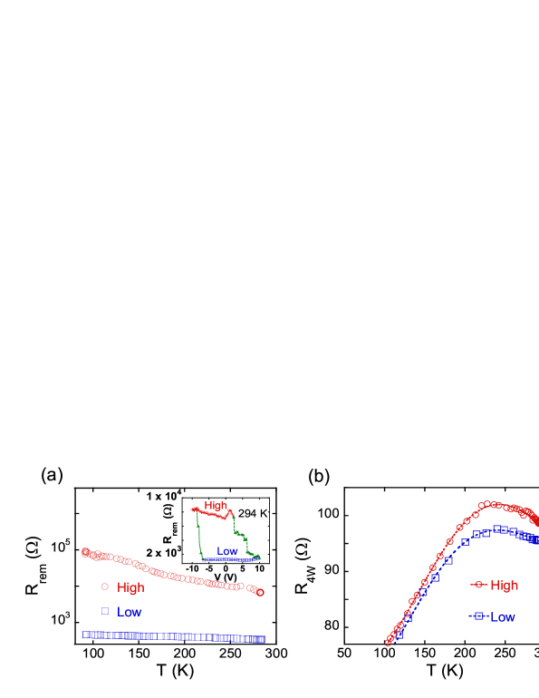
As can be observed in Fig. 2(a), was measured for both selected states before and after each IV measurement, for experiments performed at different temperatures. It is clear that no significant RS was produced along the entire series of IV measurements. The dependence of for both states (Fig. 2(b) shows the typical behavior measured before the pulsing treatments. [11] Surprisingly, the measured is different for each contact state, although is measured with contacts 3 and 4 (see Fig. 1(a) located at a macroscopic distance ( 1 mm) from the pulsed contacts 1-2. The increase of resistivity when switching from LRS to HRS is in accordance with a reduction of the local oxygen content. [13] This indicates that the pulsing affects zones far away from the interfaces, as was previously observed [14] in ceramic YBa2Cu3O7 (YBCO), probably associated to the high mobility of oxygen in these oxides [15, 16] and to its relation to the mechanism of the resistance change induced by the pulsing treatment. [4]
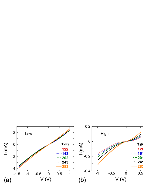
The IV characteristics for both selected states are shown in Fig. 3. Both states show non-linear effects. The LRS shows a small dependence, while the HRS shows a higher sensitivity to it. A Schottky mechanism can be ruled out as no rectifying behavior can be observed. Details of the IV characteristics are more readily apparent if one considers the derivative plotted as a function of (see Fig. 4). [17] For clarity, only the increasing negative voltage part of the IV measurement cycle was used to plot these curves (taking the absolute value of V). Indeed, the typical conduction mechanisms through metal-oxide interfaces can be easily determined by analyzing these vs curves. This is the case for an ohmic, a Langmuir-Child or a SCLC conduction, that will all show a constant ( 1, 1.5 or 2, respectively), or for a Schottky (Sch) or a Poole-Frenkel (PF) behavior that will be represented by a straight line differing in the intercept (0 for Sch, 1 for PF). [5] Our results are described by a more complex vs. curve as it can be observed in Fig. 4. Both states show for low voltages a tending to a constant value close to 1 (more clearly defined for the HRS), then a small linear region limited by the appearance of a maximum (more prominent at low temperatures and for the HRS) and a final gradual decrease.

This complex behavior can be reproduced by considering the circuit elements depicted in the inset of Fig. 4(b). This representation of the memristor by a similar arrangement of circuit elements was already done in previous papers to describe the dynamical behavior of metal-YBCO interfaces [18], and the IV characteristics of metal-manganite junctions. [19, 20]
We would like to note here that the data reported by Fu et al. [9] on the IV characteristics of Ag/La0.5Sr0.5CoO3-δ interfaces presents a similar behavior to the one reported here. Their evolves gradually with increasing V from 1 to a maximum value slightly higher than 2 and then decreases smoothly with further increasing V. Here, by considering the almost linear parts of the curve and by discarding a Schottky conduction (as mentioned, due to the lack of rectifying behavior), the non-linear element was associated with a PF conduction. A parallel ohmic element () is needed to reproduce the quasi-ohmic dependence observed at low voltages, while the ohmic element in series () should be considered to limit the non-linear conduction, producing the maximum and the concomitant decrease of observed for higher voltages. In this way, the following equations represents the IV characteristics of the proposed representation for the Ag/LSCO memristor: [21, 5]
| (1) |
with
| (2) |
where is the temperature, the Boltzmann constant, the trap energy level, the electron’s charge, the conducting area, , and the real part of the dielectric constant, the density of carriers and their mobility in the oxide, respectively, and the distance where the voltage drop is produced.
The dashed-lines plotted in Fig. 4 were obtained by fitting numerically the IV curves, by using the implicit Eq. 1. The non-trivial experimental dependence is very well reproduced by the proposed model. Only a slight difference can be noted for the highest voltages in the HRS, where seems to saturate at a value close to 1.5 instead of the expected 1. This is possibly indicating the existence of a more complex process in parallel with , like a -independent Langmuir-Child conduction due to ballistic carriers through vacuum voids or oxygen-depleted zones [5, 22]. More work is needed to address these deviations, which are beyond the scope of the present paper.
We reduced the four fitting parameters , , and to three by considering that and can be related to the measured using the fact that, for sufficiently low voltages, (see Ref. 23 for a list of typical parameters obtained for each state). Fig. 5 shows the , , , and parameters obtained from the fits. For both resistance states, a straight line is obtained when plotting Ln(A) vs 1/T, indicating that the exponential relation of with 1/T derived from the PF conduction is valid (see Eq. 2). The slope, associated with the trap potential , indicates the presence of traps [ 900 K] in the interfacial zone of the oxide for the HRS, while the flatness of the curve for the LRS points out practically their absence [ 60 K]. Similar values ( 700-1200 K) were obtained for Au/YBCO interfaces after pulsing treatments. [7] In the same way, by analyzing the intercept, it can be derived that . This indicates that not only deeper traps are created when switching from LRS to HRS but also that the resistivity of the interfacial zone, where the PF conduction develops, increases, which is probably associated with an overall reduction of the local oxygen content.

The parameter is plotted in Fig. 5(b) as times vs T, in order to represent, according to Eq. 2, the dependence of , where (with being the vacuum permittivity). As the distance , associated with the interfacial zone, is expected to be independent, and to remain practically unchanged for both states, as was reported for Au/YBCO [7], the dependence of can be directly inferred from Fig. 5(b). It can be observed that in the LRS increases with decreasing , following a step-like shape, while in the HRS it shows a tendency to saturate for temperatures below 200 K. This non-usual dependence of for a paraelectric oxide [24] was previously observed in the case of mixtures of conducting and insulating regions, which are in many cases generated intrinsically in metal-oxide interfaces [25]. This mixture of phases may give rise to a Maxwell-Wagner (MW) effect [25, 26], where the charge carriers accumulate at the border of the conducting regions, which act as very small parallel-plate capacitors, representing a very high capacitance. In this particular case, by describing the sample as composed by an interfacial region in series with the bulk (each material with different conductivity and dielectric constant), it was shown that the dielectric constant has a frequency dependence described by the Debye relaxation laws, with a static value () higher than the one at high frequencies () and a characteristic time () that follows the dependence of the resistivity of the bulk. A step in to a higher value (a shift from to ) is then predicted as is reduced when decreasing . This is particularly what it can be observed in Fig. 5(b), as in the LRS increases in correspondence to the decrease of (see Fig. 5(c), which represents the electrical connection between the interfacial zone and the bulk. In contrast, as remains insulating in the HRS (see Fig. 5(d), the obtained is weakly dependent.
Finally, becomes 100 times more insulating in the HRS while , mimics the dependence of the resistance in the LRS, but becomes semiconducting-like with a 10 times increase in the HRS. This similarity between and (T), only differing in a geometric constant that amplifies its value, was previously seen in metal interfaces with YBCO[14] and manganites[27], pointing out the generality of this process.
All these results lead us to consider that, independently of the initial oxygen content of the oxide, the Ag/LSCO interfacial region has become an oxygen-depleted zone, where the electrical transport properties are dominated by the presence of charge carrier’s traps (PF) in parallel with insulating regions (). These interfacial characteristics may represent a common feature of other metal/perovskite oxide interfaces, like Au/YBCO, were a similar behavior was observed[7], probably associated with the capacity of the metallic electrode to generate in the oxide the coexistence of conducting and insulating regions, yielding probably to a granular structure. This scenario would be similar to the one existing intrinsically for phase-separated manganites, where the coexistence of nanometric conducting and insulating regions is a feature proper of their phase separation characteristics. [28] In fact, their dielectric properties showed a behavior compatible with a MW description, as was already reported. [29, 30, 26]
In summary, the dependence of the RS properties of a Ag/LSCO interface was reported. A detailed study of the IV characteristics at different temperatures for both LRS and HRS is presented, allowing the development of an equivalent circuit model based on a non-linear PF element and two ohmic resistances. This model captures the non-trivial electrical behavior of the Ag/LSCO junction that we believe gives a general representation of other metal/perovskite oxide memristors. This model also allows to envision details of the microscopic constitution of the interfacial zone and to understand which are the specific changes produced upon the pulsing treatments.
We acknowledge financial support from CONICET PIP12-14(0930), PICT13-0788 and UBACyT14-17(20020130100036BA).
References
- [1] J. J. Yang, D. B. Strukov, and D. R. Stewart. Nature Nanotechnology, 8:13, 2013.
- [2] R. Waser, R. Dittmann, G. Staikov, and K. Szot. J. Appl. Phys., 78:6113, 2009.
- [3] A. Sawa. Materials Today, 11:28, 2008.
- [4] M. J. Rozenberg, M. J. Sánchez, R. Weht, C. Acha, F. Gomez-Marlasca, and P. Levy. Phys. Rev. B, 81:115101, 2010.
- [5] S. M. Sze and K. K. Ng. Physics of Semiconductor Devices. John Wiley & Sons, 2006.
- [6] D. S. Shang, Q. Wang, L. D. Chen, R. Dong, X. M. Li, and W. Q. Zhang. Phys. Rev. B, 73:245427, 2006.
- [7] A. Schulman, L. F. Lanosa, and C. Acha. Journal of Applied Physics, 118:044511, 2015.
- [8] M. Hamaguchi, K. Aoyama, S. Asanuma, Y. Uesu, and T. Katsufuji. Appl. Phys. Lett., 88:142508, 2006.
- [9] Y. J. Fu, F. J. Xia, Y. L. Jia, C. J. Jia, J. Y. Li, X. H. Dai, G. S. Fu, B. Y. Zhu, and B. T. Liu. Applied Physics Letters, 104(22):223505, 2014.
- [10] K. Daoudi, T. Tsuchiya, T. Nakajima, A. Fouzri, and M. Oueslati. J. Alloys Compd., 506:483, 2010.
- [11] Z. Othmen, A. Schulman, K. Daoudi, M. Boudard, C. Acha, H. Roussel, M. Oueslati, and T. Tsuchiya. Applied Surface Science, 306:60, 2014.
- [12] The same studies can be performed for the interface just by following the same steps but measuring the voltage drop V42 instead of V13. As both electrodes showed qualitatively similar results, only those for are presented here.
- [13] Bin Liu, Guiju Liu, Honglei Feng, Chao Wang, Huaiwen Yang, and Yiqian Wang. Materials and Design, 89:715, 2016.
- [14] C. Acha and M. J. Rozenberg. J. Phys.: Condens. Matter, 21:045702, 2009.
- [15] A. Chroneos, R.V. Vovk, I.L. Goulatis, and L.I. Goulatis. Journal of Alloys and Compounds, 494(1–2):190 – 195, 2010.
- [16] Ho-Il Ji, Jaeyeon Hwang, Kyung Joong Yoon, Ji-Won Son, Byung-Kook Kim, Hae-Won Lee, and Jong-Ho Lee. Energy Environ. Sci., 6:116–120, 2013.
- [17] A. Bozhko, M. Shupegin, and T. Takagi. Diamond and Related Materials, 11:1753, 2002.
- [18] C. Acha. J.Phys.D: Appl.Phys., 44:345301, 2011.
- [19] F. Gomez-Marlasca, N. Ghenzi, A. G. Leyva, C. Albornoz, D. Rubi, P. Stoliar, and P. Levy. Journal of Applied Physics, 113(14):144510, 2013.
- [20] Although the measurements were performed at low frequencies, in a stationary regime, the capacitances of the interfacial zone () and the bulk () were also considered in order to take into account the dielectric behavior of the device. [25].
- [21] J. G. Simmons. Phys. Rev., 155:657, 1967.
- [22] Siwapon Srisonphan, Yun Suk Jung, and Hong Koo Kim. Nat Nano, 7, 2012.
- [23] See supplemental material at [URL will be inserted by AIP] for a list of the typical parameters obtained for both states.
- [24] B. D. Silverman and R. I. Joseph. Phys. Rev., 129:2062, 1963.
- [25] P. Lunkenheimer, V. Bobnar, A. V. Pronin, A. I. Ritus, A. A. Volkov, and A. Loidl. Phys. Rev. B, 66:052105, 2002.
- [26] P. Lunkenheimer, S. Krohns, S. Riegg, S.G. Ebbinghaus, A. Reller, and A. Loidl. The European Physical Journal Special Topics, 180:61, 2010.
- [27] M. Quintero, P. Levy, A. G. Leyva, and M. J. Rozenberg. Phys. Rev. Lett., 98:116601, 2007.
- [28] E. Dagotto, T. Hotta, and A. Moreo. Physics Reports, 344:1, 2001.
- [29] G. Garbarino, C. Acha, P. Levy, T. Y. Koo, and S-W. Cheong. Phys. Rev. B, 74:100401(R), 2006.
- [30] J. Rivas, J. Mira, B. Rivas-Murias, A. Fondado, J. Dec, W. Kleemann, and M. A. Señaris-Rodríguez. Applied Physics Letters, 88(24):242906, 2006.