Invisibility Cloak Printed on a Photonic Chip
Invisibility cloak capable of hiding an object can be achieved by properly manipulating electromagnetic field. Such a remarkable ability has been shown in transformation and ray optics. Alternatively, it may be realistic to create a spatial cloak by means of confining electromagnetic field in three-dimensional arrayed waveguides and introducing appropriate collective curvature surrounding an object. We realize the artificial structure in borosilicate by femtosecond laser direct writing, where we prototype up to waveguides to conceal millimeter-scale volume. We characterize the performance of the cloak by normalized cross correlation, tomography analysis and continuous three-dimensional viewing angle scan. Our results show invisibility cloak can be achieved in waveguide optics. Furthermore, directly printed invisibility cloak on a photonic chip may enable controllable study and novel applications in classical and quantum integrated photonics, such as invisualising a coupling or swapping operation with on-chip circuits of their own.
Introduction
Transformation optics is a prevalent approach to modify material parameters, carefully constructing artificial material and manipulating electromagnetic wave Pendry2006 ; Leonhardt2006 . Due to the enormous difficulties in the realization of cloaking, scientists have been seeking various simplified models Schurig2006 ; Cai2007 ; Li2008 ; Kildishev2008 ; Leonhardt2009 ; Chen2010 to approach the prefect cloaking. Among those methods, Schuig et al. Schurig2006 use artificially structured metamaterial to fulfill the dimension-reduced cloaking scheme which could only cloak the light at some specific frequencies and polarizations. To broaden the operating frequency range Li2008 ; Kildishev2008 ; Leonhardt2009 , the carpet cloak is introduced to operate at microwave Liu2009 ; Ma2010 and optical Valentine2009 ; Gabrielli2009 ; Ergin2010 frequency bands. Metamaterials are also applied to achieve a skin cloak which can hide volumetric objects at optical frequencies Ni2015 . In diffusive light scattering medium where light does not conform to the ballistic propagation, broadband macroscopic cloak made of thin shells of metamaterial is realized in three dimensions, according to Fick′s equation Schittny2014 .
Ray optics provides a new way of concealing macroscopic objects by using calcite crystal Zhang2011 ; Chen2011 and standard optical devices such as lens Choi2014 and prism Chen2013 , which can guide light though a predefined path by Snell′s Law. We introduce a distinctive broadband cloaking scheme in waveguide optics that can be applied on a photonic chip. To be specific, light can be confined in the core of waveguide with higher refractive index associated with a modest curve, which shows its capability of guiding and manipulating light field in an arrayed configuration. Within the tolerance of curvature, a waveguide is bended to circumvent a central region. Optical information through the waveguide is acquired at the output while the exact propagation path remains confidential, which allows hidden objects to exist in the areas rounded by waveguides. The artificial structure requires a waveguide fabrication technique in three-dimensional space, which can be met by the intrinsic processing capacity of femtosecond laser writing Davis1996 ; Nolte2003 ; Meany2015 . A refractive index contrast can be generated via nonlinear absorption of femtosecond laser in transparent materials, where a trajectory of laser focus transforms to a waveguide. Elaborate control of the trajectory enables complex optical circuits Crespi2012 ; Meany2015 ; Chaboyer2015 as well as three-dimensional configuration Nolte2003 ; Chaboyer2015 .
Results
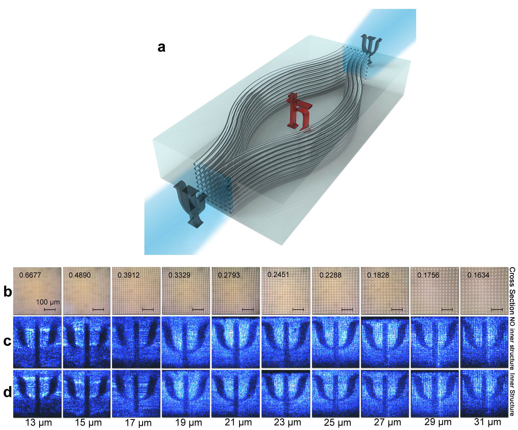
As a cloaking scheme, two prerequisites should be met: a clear image transfer and a hidden inner structure Xu2014 . Foreground mask featured is set before the entrance window of the photonic chip and this image is expected to be soundly transported through the chip without any interference with an inner structure . In order to cloak the structure inside a chip, which is fabricated with a high power laser, we prototype up to waveguides in three dimensions along a spindle path opening up the central space for the to be hidden in (Fig.1a).
In this section, we characterize the cloaking structures by different pitches and optimize the performance with the introduced similarity assessment. Tomography analysis is applied to unveil the evolution of light field in the optimal one. In the end, we benchmark the robustness of the cloaking device with a continuous three-dimensional viewing angle scan.
Cloaking performance optimization
The spindle of tightly bounded waveguides seems to be a favorable choice to obtain a high resolution image. However, considering the interactions between waveguides, the pitch is obviously a crucial parameter to determine the clarity of image transfer. In our experiment, we fabricate configurations of spindles with different pitches ranging from to and the corresponding cross sections captured using a objective lens with a numerical aperture of 0.4 and eyepieces are exhibited in Fig.1b. A Gaussian beam () is radiated through the mask at the input of the spindle and collected at the output by a CCD camera, as shown in Fig.1c, d. Each configuration contains two sets: with (Fig.1d) and without (Fig.1c) the inner structure. As illustrated in Fig.1c and d, various outputs are observed owing to different pitches. In order to evaluate their performances, a uniform statistical criterion should be set up. Therefore we introduce the normalized cross correlation () Lewis1995 ; Halimeh2011 , a common and convenient assessment of the similarity between two image patterns with the basic idea to compare the grey scale of each corresponding pixel between two images. Specifically, when images are converted into grey matrixes, between image a and b can be represented as:
| (1) |

where represents the pixel of the image. , is the average value of all the grey scale of pixels of a and b, respectively. According to the definition, the ranges from to ; the closer to the value is, the more similar two figures are to each other.
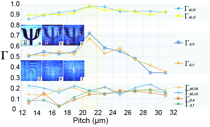
Firstly we compare the similarity of between the one passing through the waveguides with different pitches and the one only through the chip substrate (Fig.2b(c) and Fig.2a). The results (;) sketch that the value increases steadily and reaches the peak at the pitch value of and then decreases with the pitch getting larger. The optical coupling (crosstalk) distorts the information of the light field propagating in the waveguide when the waveguides get too close to each other. It conforms to a monotonous tendency, which optical coupling decreases by about with every pitch increase of , according to our calculation. Due to the elliptical cross section (see Fig.1b), the crosstalk distortion is especially intensive in the vertical direction. On the other hand, a larger pitch constraints the total volume of information in virtue of the lower waveguide density. We calculate the duty cycle, the ratio of the total cross sectional area that the waveguides occupy to the CCD active area, to quantitatively show the waveguide density. (shown in Fig.1b).
As referred in the first result (See line ; in Fig.2), where is regarded as the optimal pitch for transmitting the image, the maximum value is still moderately large, which can be attributed to the overweight of the background (the region on the image except the ) in the calculation of . To estimate the influence of the background, we extract region ii in Fig.2a-c and calculate the , as shown in Fig.2(; ). The result shows that the similarity of the background between different images remains at a low level (within the range of ).
In view of the low weight of background noise visually, we clip the structure of (Region i in Fig.2a-c) from a uniform background and then re-calculated the . As expected, the values increase prominently, reaching the peak at (Fig.2(; )). Furthermore, it is the consequence of the inevitable dissipation of light between waveguides that the maximum of , peaking at , still cannot reach . Actually, the pitch of reaches the image standard as high as a retina image.
Subsequently, we remove the foreground mask and compare the similarity between the output image of the chip with the uncloaked inner structure (Fig.2d) and the one without the cloaked structure (Fig.2e), the one with the cloaked structure (Fig.2f), respectively. The result shows the values fluctuate around , which is numerically hard to differentiate from background noise (see Fig.2 (; )). Indeed, the inner structure has been cloaked and cannot be distinguished through calculating the similarity, which obviously accords with our visual result.
Tomography analysis of on-chip cloaking
To reveal the evolution of light field in the printed cloak, tomography analysis is applied to the mechanism of cloaking. We cut the chip transversely, record the data from the output and compare these experiment results with simulation ones.
We simulate this experiment by a commercial software RSoft (Beam type: Gaussian, wavelength: , refractive index ) and derive the distribution of the light field. As shown in Fig.3, after the beam incidence, most light circumvents the cloaked area along the waveguides, while the rest is scattered by the bulk of the chip and forms the weak white noise in the background. Also we find the light distribution in the output is quite similar with the one in the input, which means little information may have lost after the transmission.
Inspired by the widely used tomography in biological science Fujimoto1995 ; Low2006 , we perform a tomography on our cloaking chip by grinding the chip to a predefined length, which takes hours for each millimeter removal on a polisher. As the chip gets shorter, by observing the cross section pattern, the process of the projection image splitting into two parts gradually apart from each other and then combining into one again is experimentally reproduced. Comparing the numerical results of the processed intensity distribution along the lateral axis (Fig.3b), we can observe that the numerical one is more fluctuant, which is because the stray light smooths the fluctuation in the experiment.
Three-dimensional capacity of cloaking.
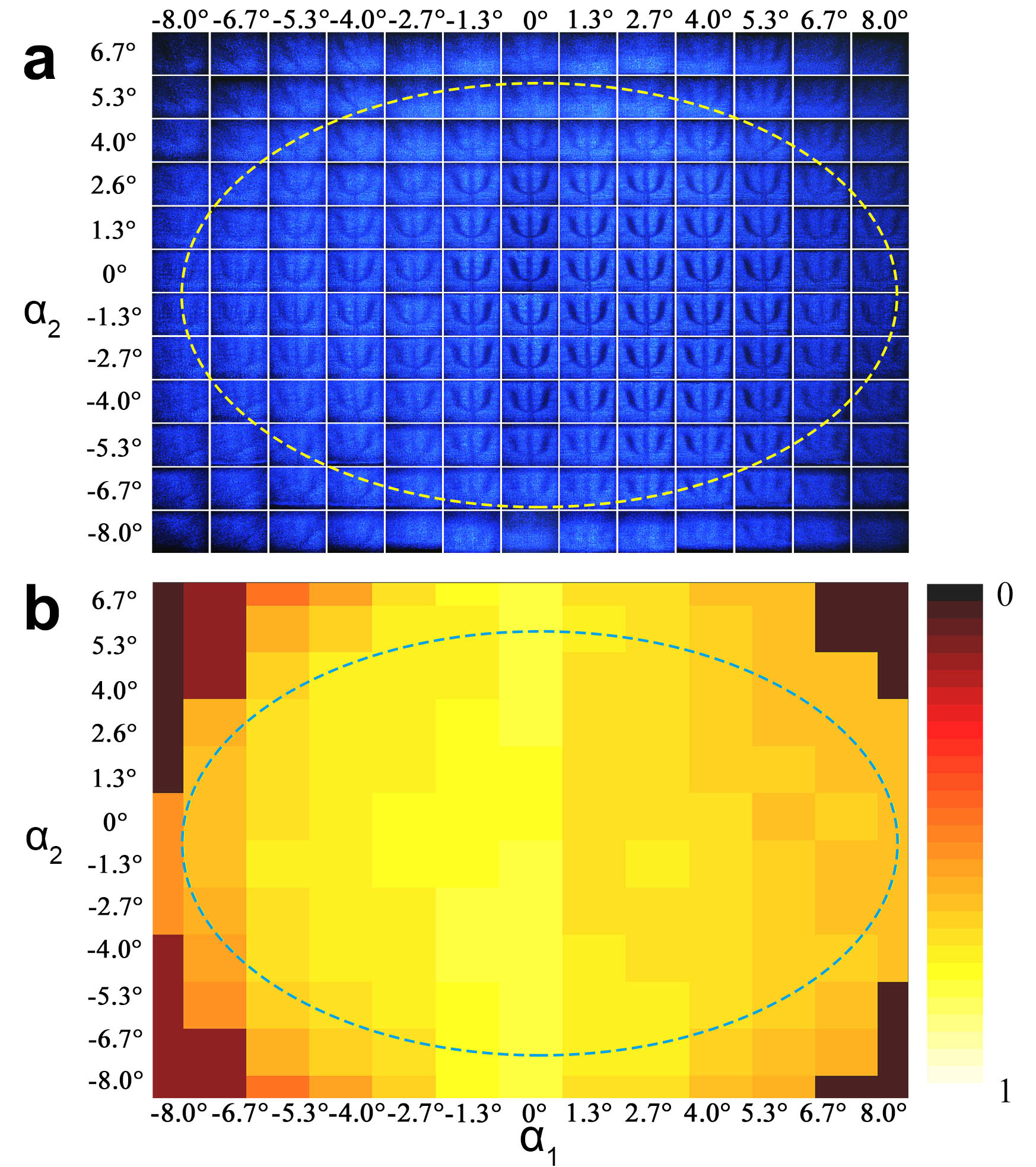
Three-dimensional capacity is frequently employed to benchmark the performance of a cloaking approach. In our experiment, while our cloaking approach is only implemented in one dimension to demonstrate its feasibility, the same method can be extended to three dimensions with higher complexity of waveguide arrangement and larger number of printed waveguides. We should note that cloaking in one dimension is not that trivial in certain scenarios. For instance, the chips are packaged leaving only some specific access to the public. The components placed at appropriate locations can be well hidden on the chip in the observation direction. Interestingly, even our one-dimensional configuration has its three-dimensional capacity of cloaking in a cone, which can be understood as an effect of collective numerical aperture of waveguides.
Therefore, the tolerance for viewing angle on the chip, which shows three-dimensional capacity of cloaking, is also investigated Chen2013 ; Choi2014 . We change the view direction by adjusting the lens behind the cloaking chip ( pitch, with the inner structure) multi-directionally and align the output image with the corresponding direction as shown in Fig.4. The sharpness, brightness and visibility decrease as the viewing angle gets large, though the does not distort. An elliptical-like region spanning laterally and vertically outlines the tolerance for viewing angle. Besides, the limited angle that we derive above conforms to the numerical aperture theory of an individual multimode fiber. It is remarkably interesting that, the inner structure is cloaked so well that even if the obliqueness of the viewing angle is large enough to affect the image transmission, no parts can be observed. In addition, output powers in Fig.4a are measured and plotted correspondingly (see Fig.4b) which describes the energy distribution in the output light cone.
Discussion
Length difference of waveguides introduces phase distortion site by site. In our experiment, imperfect collective bending of waveguides may generate site-dependent length difference and therefore differential phases. A phase-preserved cloak Xu2012 ; Yu2013 ; Xu2015 can be realized by setting the difference to be integral times of in the fabrication process of femtosecond direct writing.
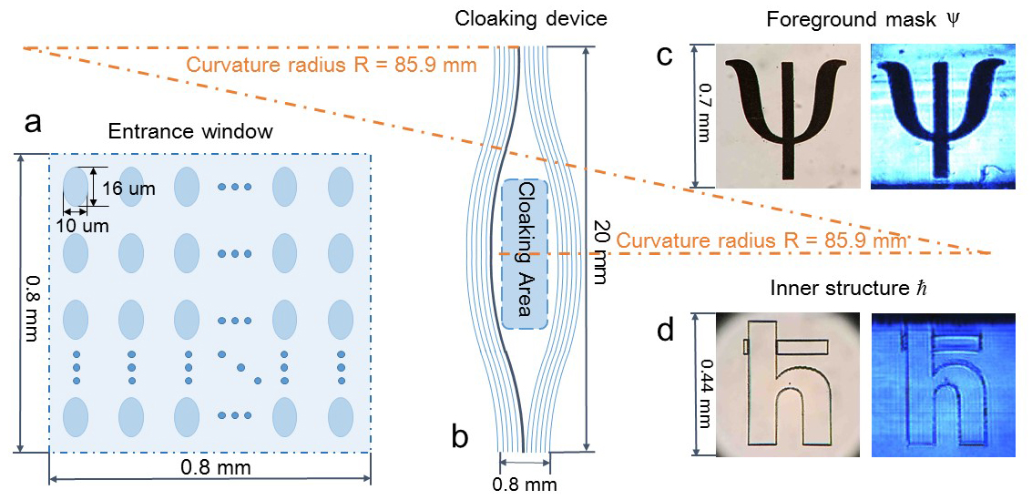
We further discuss on the capacity of the cloaking structure. In our configuration, we implement the cloaking structure in the curvature radius (Definition of raidus in attached supplmentary information) with refractive index contrast to obtain an optimal cloaking performance in a hidden region in size of . With the decrease of curvature radius, larger bending loss is introduced.
In conclusion, we have presented the first experimental demonstration of invisibility cloak in waveguide optics that can hide millimeter-scale structure inside a photonic chip. The printed waveguides confine and guide light field in a three-dimensional array, and evolve with collective curvature in the propagating direction to mimic the Poynting vector in transformation-optics-based cloak Pendry2006 . A larger invisible volume is attainable with tightly bending cloak spindle of high refractive index contrast Eaton2011 and rearrangement of waveguides. The quality of image transfer that benchmarks the performance of cloak can be upgraded by increasing the waveguide density and suppressing crosstalk distortion simultaneously, which is achievable if we can manipulate all the phases of evanescent light interference between waveguides Chaboyer2015 . The on-chip image transfer itself may stimulate novel applications in deep space exploration Bland2011 and biological sensing Walt2002 . Furthermore, the printed cloak allows backdoor operations like swap or coupling isolated from observers, representing an emerging problem of information security and hacking on a photopic chip.
Methods
Waveguide inscription and laser processing
A femtosecond laser () with pulse duration and repetition rate is frequency doubled to and directed into an spatial light modulator(SLM) to create burst trains which is focused on a borosilicate substrate () with a objective lens with a numerical aperture of 0.55 to fabricate several thousand spindle waveguides (-radius curves with 1.5mm-long straight design at both ends; refractive index increase of in the borosilicate substrate ) at a constant velocity of . Array is formed with a cross section size of and great efforts have been made to process depth independent waveguides through power and SLM compensation. An inner structure of reduced Planck constant whose visibility is guaranteed by a high power laser direct writing back and forth hundreds of times is located in cloaking area with the size of (See Fig.5 for overall design parameters).
Correlation Coefficient value acquisition
Since we only concern about the in images a and b (See Eq.1), the exact CCD image clipping is necessary. To eliminate the error caused by the slight shift of , we make a clip of image a with a resolution matrix of , and then crop a smaller box of image b with the matrix of in the same way. Transforming the RGB matrix into grey scale, we compare the matrix extracted from b with every submatrix of a. The final normalized correlation coefficient value between a and b, , is chosen to be the maximum of the results. Specifically in our demonstration, we crop image a of pixels and image a of pixels. The value is chosen to be the maximum of results.
Simulation of light field evolution
A commercial Beam Propagation Method software is used to test the cloaking scheme qualitatively in advance. We build a glass block with volume of , transparent boundary condition, refractive index as a photonic chip where 3838 waveguides (the size of each cross section is ) are imbedded with index increase of 0.0015. All other geometry conforms to the fabrication structure. A beam, cut from a non-polarized Gaussian beam of wavelength by a square mask, is launched on the cloaking chip. All simulation results are illustrated in Fig.3a and b.
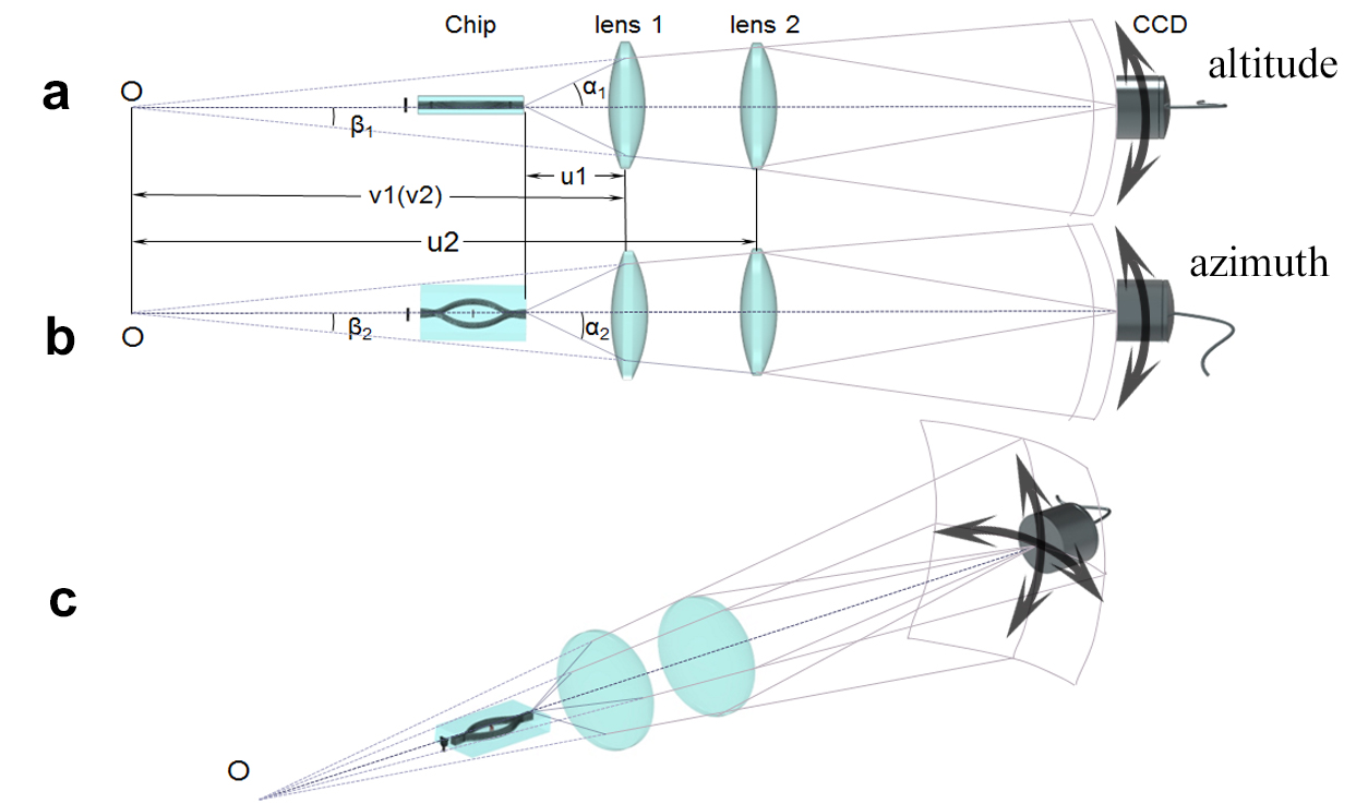
Three-Dimensional Capacity Characterization
A Gaussian beam (wavelength ; beam waist ) through the mask is radiated at the input of the spindle and the output light information is collected by two sequent lenses placed behind the chip for imaging, as shown in Fig.6. The key parameter, the viewing angle related to the output of the chip cannot be measured directly unless we move the lens 1 after each measurement, which leads to vast workload of readjustment. Since the light is paraxial, we can map the output of the waveguide to the point O by lens 1 and measure the corresponding object distance() and image distance(). Thus, can be calculated by the indirect measurement of angle for the relation between and is given by
| (2) |
where represents azimuth and elevation angles. Since images can only be formed when lens 2 is within the light cone, we shift lens 2 both in azimuth and altitude direction with a corresponding adjustment of the CCD to catch the image simultaneously. After recording the shifting distance (Not shown in Fig.5) of lens 2 and the length of , we can get the corresponding angle :
| (3) |
Substitute (3) into (2), we get the expression of viewing angle :
| (4) |
In addition, we have also measured the output powers in every combination of azimuth and elevation angles and plotted in Fig.4b. This energy distribution demonstrates a radiational decreasing tendency of energy from the center to the edge in the output light cone, which shows a visually great agreement with the radiational decreasing of clearity in the result of Fig.4a.
Acknowledgments: This research leading to the results reported here was supported by the National Natural Science Foundation of China under Grant No.11374211, the Innovation Program of Shanghai Municipal Education Commission, Shanghai Science and Technology Development Funds, and the open fund from HPCL (No.201511-01). X.-M.J. acknowledges support from the National Young 1000 Talents Plan.
References
- (1) Pendry, J. B. Controlling electromagnetic fields. Science 312, 1780–1782 (2006).
- (2) Leonhardt, U. Optical conformal mapping. Science 312, 1777–1780 (2006).
- (3) Schurig, D. et al. Metamaterial electromagnetic cloak at microwave frequencies. Science 314, 977–980 (2006).
- (4) Cai, W., Chettiar, U. K., Kildishev, A. V. & Shalaev, V. M. Optical cloaking with metamaterials. Nat. Photonics 1, 224–227 (2007).
- (5) Li, J. & Pendry, J. B. Hiding under the carpet: A new strategy for cloaking. Phys. Rev. Lett. 101, 203901 (2008).
- (6) Kildishev, A. V., Cai, W., Chettiar, U. K. & Shalaev, V. M. Transformation optics: approaching broadband electromagnetic cloaking. New J. Phys. 10, 115029 (2008).
- (7) Leonhardt, U. & Tyc, T. Broadband invisibility by non-Euclidean cloaking. Science 323, 110–112 (2009).
- (8) Chen, H., Chan, C. T. & Sheng, P. Transformation optics and metamaterials. Nat. Mater. 9, 387–396 (2010).
- (9) Liu, R. et al. Broadband ground-plane cloak. Science 323, 366–369 (2009).
- (10) Ma, H. F. & Cui, T. J. Three-dimensional broadband ground-plane cloak made of metamaterials. Nat. Commun. 1, 21 (2010).
- (11) Valentine, J., Li, J., Zentgraf, T., Bartal, G. & Zhang, X. An optical cloak made of dielectrics. Nat. Mater. 8, 568–571 (2009).
- (12) Gabrielli, L. H., Cardenas, J., Poitras, C. B. & Lipson, M. Silicon nanostructure cloak operating at optical frequencies. Nat. Photonics 3, 461–463 (2009).
- (13) Ergin, T., Stenger, N., Brenner, P., Pendry, J. B. & Wegener, M. Three-dimensional invisibility cloak at optical wavelengths. Science 328, 337–339 (2010).
- (14) Ni, X., Wong, Z. J., Mrejen, M., Wang, Y. & Zhang, X. An ultrathin invisibility skin cloak for visible light. Science 349, 1310–1314 (2015).
- (15) Schittny, R., Kadic, M., Buckmann, T. & Wegener, M. Invisibility cloaking in a diffusive light scattering medium. Science 345, 427–429 (2014).
- (16) Zhang, B., Luo, Y., Liu, X. & Barbastathis, G. Macroscopic invisibility cloak for visible light. Phys. Rev. Lett. 106, 033901 (2011).
- (17) Chen, X. et al. Macroscopic invisibility cloaking of visible light. Nat. Commun. 2, 176 (2011).
- (18) Choi, J. S. & Howell, J. C. Paraxial ray optics cloaking. Opt. Express. 22, 29465 (2014).
- (19) Chen, H. et al. Ray-optics cloaking devices for large objects in incoherent natural light. Nat. Commun. 4 (2013).
- (20) Davis, K. M., Miura, K., Sugimoto, N. & Hirao, K. Writing waveguides in glass with a femtosecond laser. Opt. Lett. 21, 1729 (1996).
- (21) Nolte, S., Will, M., Burghoff, J. & Tuennermann, A. Femtosecond waveguide writing: a new avenue to three-dimensional integrated optics. Appl. Phys. A Mater. Sci. Process. 77, 109–111 (2003).
- (22) Meany, T. et al. Laser written circuits for quantum photonics. Laser Photon. Rev. 9, 363–384 (2015).
- (23) Crespi, A. et al. Measuring protein concentration with entangled photons. Appl. Phys. Lett. 100, 233704 (2012).
- (24) Chaboyer, Z., Meany, T., Helt, L. G., Withford, M. J. & Steel, M. J. Tunable quantum interference in a 3D integrated circuit. Sci. Rep. 5, 9601 (2015).
- (25) Xu, L. & Chen, H. Conformal transformation optics. Nat. Photonics 9, 15–23 (2014).
- (26) Lewis, J. Fast template matching. Vis. Interface 120–123 (1995).
- (27) Halimeh, J. C., Schmied, R. & Wegener, M. Newtonian photorealistic ray tracing of grating cloaks and correlation-function-based cloaking-quality assessment. Opt. Express 19, 6078 (2011).
- (28) Fujimoto, J. G. et al. Optical biopsy and imaging using optical coherence tomography. Nat. Med 1, 970–972 (1995).
- (29) Low, A. F., Tearney, G. J., Bouma, B. E. & Jang, I.-K. Technology insight: optical coherence tomography—current status and future development. Nat. Clin. Pract. Cardiovasc. Med. 3, 154–162 (2006).
- (30) Xu, H., Zhang, B., Yu, T., Barbastathis, G. & Sun, H. Dielectric waveguide bending adapter with ideal transmission: practical design strategy of area-preserving affine transformation optics. Journal of the Optical Society of America B 29, 1287 (2012).
- (31) Yu, Y. et al. Controlled scalable synthesis of uniform, high-quality monolayer and few-layer MoS2 Films. Sci. Rep. 3 (2013).
- (32) Xu, S. et al. Broadband surface-wave transformation cloak. Proceedings of the National Academy of Sciences 112, 7635–7638 (2015).
- (33) Eaton, S. M., Ng, M. L., Osellame, R. & Herman, P. R. High refractive index contrast in fused silica waveguides by tightly focused, high-repetition rate femtosecond laser. J. Non. Cryst. Solids. 357, 2387–2391 (2011).
- (34) Bland-Hawthorn, J. et al. A complex multi-notch astronomical filter to suppress the bright infrared sky. Nat. Commun. 2, 581 (2011).
- (35) Walt, D. R. Imaging optical sensor arrays. Curr. Opin. Chem. Biol. 6, 689–695 (2002).