Time-reversal-breaking topological phases in antiferromagnetic Sr2FeOsO6 films
Abstract
In this work, we studied time-reversal-breaking topological phases as a result of the interplay between antiferromagnetism and inverted band structures in antiferromagnetic double perovskite transition-metal Sr2FeOsO6 films. By combining the first-principles calculations and analytical models, we demonstrate that the quantum anomalous Hall phase and chiral topological superconducting phase can be realized in this system. We find that to achieve time-reversal-breaking topological phases in antiferromagnetic materials, it is essential to break the combined symmetry of time reversal and inversion, which generally exists in antiferromagnetic structures. As a result, we can utilize an external electric gate voltage to induce the phase transition between topological phases and trivial phases, thus providing an electrically controllable topological platform for the future transport experiments.
I Introduction
Recent years have witness the rapid development of the field of topological states of matter, due to its importance in our understanding on quantum states of matter, as well as the potential applications in electronic devices with low dissipations Qi and Zhang (2011); Hasan and Kane (2010) and topological quantum computation Kitaev (2003); Nayak et al. (2008). The classification of topological states depends on the presence or absence of certain type of symmetry Schnyder et al. (2008); Ryu et al. (2010). Quantum anomalous Hall (QAH) phase Qi et al. (2006); Yu et al. (2010) and chiral topological superconductor (CTSc) Alicea (2012) are two examples of topological states in absence of time reversal (TR) symmetry (denoted as ). The realization of these time-reversal-breaking (TRB) topological states in ferromagnetic (FM) materials, as a consequence of the interplay of exchange coupling, spin-orbit coupling (SOC) and inverted band structures, has motivated intensive theoretical and experimental research activities. The QAH effect has been observed experimentally in magnetically doped (Bi,Sb)2Te3 films with long-range ferromagnetic order Chang et al. (2013, 2015). Evidences of CTSc have been identified in Sr2RuO4 -wave superconductors (SCs) Mackenzie and Maeno (2003) or other SC system in proximity to FM or under magnetic fields Mourik et al. (2012); Nadj-Perge et al. (2014). Since any magnetism can break TR symmetry, it is natural to ask if TRB topological phases can be realized in other magnetic structures, in particular anti-ferromagnetic (AFM) materials. A few recent theoretical works started exploring topological phases in AFM systems Liang et al. (2013); Wu et al. (2015); Zhou and Sun (2016); Qiao et al. (2014); Zhou et al. (2016). However, the required condition is still unclear. More importantly, superconductivity is incompatible with ferromagnetism, but it can coexist with anti-ferromagnetism Bennemann and Ketterson (2008). Thus, our understanding of the interplay between topologically non-trivial band structures and anti-ferromagnetism is important for the search of new topological superconducting materials.
In this work, we studied TRB phases in a two dimensional (2D) AFM transition metal perovskite material – Sr2FeOsO6 thin film – on top of insulating or superconducting substrates. With a realistic tight-binding model, we demonstrate that both the anomalous Hall (AH) and CTSc states can be realized in this material by applying an external electric gate voltage to the film. The combined symmetry, where denotes inversion symmetry, plays an essential role since it can protect a double degeneracy at each momentum in the Brillouin zone (BZ), and forbid the presence of the AH and CTSc states. Since the symmetry can be broken by an external electric gate voltage, this allows for an electric switch between different TRB topological states. We map out the phase diagram of various CTSc phases as a function of external gate voltages and chemical potential, based on which one can construct junction structures to detect chiral Majorana fermions.
II Sr2FeOsO6 films
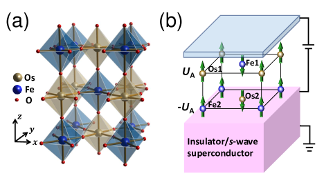
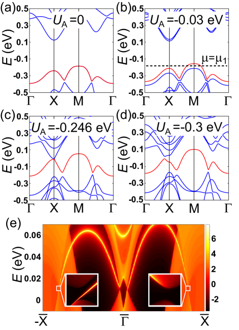
The material Sr2FeOsO6 belongs to a family of transition metal double perovskites , in which could be an alkali, alkaline earth, or rare earth atom, while and are two different transition metal atoms Paul et al. (2013a). As shown in Fig. 1(a), Sr2FeOsO6 crystalizes into an well-order tetragonal lattice with the and forming corner-sharing octahedra. Recent experiments reveals Paul et al. (2013b, a); Feng et al. (2013) that Sr2FeOsO6 is an AFM semiconductor with two magnetic phase transitions at 140 K and 67 K. Both the higher and lower temperature phases are AFM, in which magnetic moments of Fe () and Os () atoms align along the direction according to the neutron diffraction Paul et al. (2013a). Magnetic sites Fe and Os couple in an AFM way inside one checkerboard atomic layer in the plane and two adjacent atomic layers form a double layer configuration by the FM coupling. Further FM coupling between neighboring double layers along the axis leads to the higher temperature phase, while the AFM coupling between double layers gives rise to the lower temperature phase Paul et al. (2013a); Kanungo et al. (2014). In this work, we consider the principle double layers of Sr2FeOsO6 with out-of-plane magnetic moments aligned in the in-plane AFM ordering, as shown in Fig. 1(b). Low energy physics are dominated by the orbitals of Fe and Os atoms, and thus we only focus on these two atoms, which form a layered checkerboard lattice for each layer. For a bilayer lattice, there are four atoms in one unit cell, denoted as and in the top layer and and in the bottom layer. The magnetic moments of and atoms point up along the direction, while those of and atoms point down (Fig. 1(b)). Based on the maximum localized Wannier function method Marzari and Vanderbilt (1997); Souza et al. (2001), we construct a realistic tight-binding Hamiltonian, labeled by , with all five -orbitals of Fe atoms and the part (three orbitals) of Os -orbitals. We justify our tight-binding model by comparing the bulk energy dispersion with that from the first principles calculations and a good agreement is found, as shown in the Appendix A. The eigen-energy spectrum of the bilayer system can be obtained by solving the eigen equation of this Hamiltonian (16 orbitals and two spins), as shown in Fig. 2(a), for external gate voltage . Here the potential induced by an external gate voltage is assumed to be on the top layer and on the bottom layer. From Fig. 2(a), we find that the conduction band minimum appears at X (or equivalent Y) while the valence band maximum at M is about tens of meV higher than that at X (or Y), giving rise to an indirect band gap. An intriguing feature is that all the bands are doubly degenerate at each momentum, similar to the case of Kramer’s degeneracy in a TR invariant system Dresselhaus et al. (2007). Although there is no individual or symmetry, the combined symmetry exists, which reverses spin and interchanges layers, but preserves momentum, thus leading to the double (spin) degeneracy. This is quite similar to the Kramer’s degeneracy, and forbids the occurrence of non-zero Hall conductance (or equivalently non-zero Chern number). Therefore, it is essential to split this double degeneracy by breaking symmetry to achieve any TRB topological phase. We notice this degeneracy can be split by introducing an electric field along the direction to break symmetry. Below we will demonstrate that this strategy allows us to realize the AH phase and CTSc phase in thin films of Sr2FeOsO6.
III Anomalous Hall phase
We first study the case without superconductivity. We only focus on the X and Y points with a direct band gap (Fig. 2(a)). By applying a non-zero asymmetric potential (Fig. 2(b), (c) and (d)), double degeneracy for both conduction and valence bands are split. This splitting greatly reduces band gap (Fig. 2(b) and (c)), and even reverses band ordering at X (Fig. 2(d)), leading to band inversion. Band inversion can result in topological phase transition in the field of topological insulators Qi and Zhang (2011); Hasan and Kane (2010). Thus, we expect that band structure in Fig. 2(d) is topologically nontrivial. We can use Chern number, defined as , where (the summation is taken over all of the occupied bands), to characterize topological nature of our system, and direct calculation shows that the Chern number is for eV and for eV. Furthermore, we study the low-energy effective theory. Let us label two valence bands at X as and and two conduction bands as and . The first principles calculations show that originates from , is dominated by , mainly consists of , and is characterized by . When the asymmetric potential is applied, the band inversion occurs between and . On the basis of , the effective Hamiltonian is
| (1) |
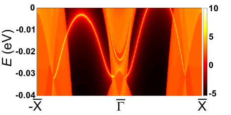
where , and are material dependent parameters. We recognize this model as a 2D massive Dirac Hamiltonian and the band inversion, which is described by the sign reverse of the mass , changes the Chern number by . Therefore, the Chern number for eV should be , taking into account the band inversion at both X and Y. Thus, we conclude that the Hall conductance should be for eV. This conclusion is further supported by the direct calculation of edge states in the ribbon configuration based on the iterative Green function method Sancho et al. (1985). Indeed, we find two chiral edge states at one edge of the ribbon (See Fig. 2(e) and its inset). Since the valence band maximum at M is higher than that at X or Y, electrons may transfer from valence bands at M to conduction bands at X and Y, leading to electron pockets at X and Y and hole pockets at M. The present of bulk carriers will destroy the quantization of Hall resistance. Thus, a large, instead of quantized, Hall resistance is expected in experiments. In addition, the scattering between electron pockets at X and Y may lead to charge (or spin) density wave. But we emphasize that topological nature of the system will not be changed once the band gap remains under charge density wave (see Appendix B). Although we consider bilayer film for simplicity, our results also exist for other film thickness (see the calculation for four-layer films in the Appendix C). We emphasize that splitting spin degeneracy by breaking the symmetry is essential and this strategy can be applied to other anti-ferromagnetic system.
IV Chiral Topological Superconducting phase
Next we will study this system on top of a superconducting substrate with the -wave singlet pairing and search for CTSc. The key idea is to induce effective triplet SC from singlet SC as a result of the coexistence of magnetism and SOC in the Sr2FeOsO6 film. Similar idea has been applied to CTSc in half-metals in proximity to a SC Lee (2009); Chung et al. (2011), where interfacial Rashba SOC flips electron spin and converts singlet pairing to triplet pairing. The advantage here is that anti-ferromagnetism and SOC coexist for Os atoms and can naturally lead to pairing conversion. Below we will demonstrate that CTSc can be realized and controlled by tuning asymmetric potential and chemical potential .
To simulate superconducting proximity effect, we consider the Bogoliubov-de Gennes (BdG) Hamiltonian
| (4) |
in which is the tight-binding model, is a diagonal matrix with non-zero diagonal elements to describe the proximity induced -wave pairing for -orbitals of Fe2 and Os2 atoms at the bottom layer. We also define a Chern number, , where , to describe topological property of the BdG Hamiltonian, where is eigen wave functions of and the summation is taken over all of the hole bands. The Chern number for is not the same as for . For the pairing potential , one can show that the electron part and the hole part possess the same Chern number and thus Qi et al. (2010). When , there is no simple relation between and .
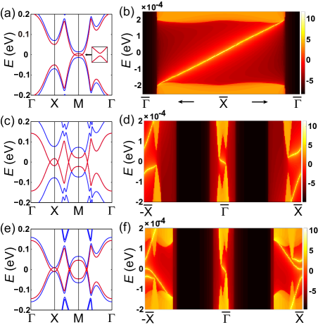
Eigen energies of can be extracted by solving the eigen-equation (4) and a typical energy dispersion is shown in Fig. 3(a). The Fermi energy is tuned to the valence bands due to the rich physics in this regime. Due to the particle-hole symmetry of , the electron bands are symmetric to the corresponding hole bands with respect to Fermi energy (corresponding to zero energy in Fig. 3(a) for ). A superconducting gap induced by is shown in the inset of Fig. 3(a). The key to realize CTSc is to identify the parameter regime in which band crossings between electron and hole bands only occur for odd number of times. When , all the bands are doubly degenerate due to the symmetry and the number of band crossing must be even. Therefore, the resulting superconducting phase must be trivial. This argument again suggests that breaking symmetry by a non-zero is essential. Fig. 3(a), (c) and (e) are for three different sets of parameters ( and ). In Fig. 3(a) with eV, eV and eV, a non-zero split two bands at M and the Fermi energy is tuned to cross only one band around M. In this case, the Chern number for the corresponding superconducting phase with one chiral Majorana edge mode, as confirmed by the direct calculation of edge modes on a slab configuration in Fig. 3(b). We can further construct an effective model for this superconducting phase based on the theory of invariant. We label two valence band states at M as and , of which is dominated by the state, while is given by . For , only one term is allowed (See Appendix D), where and are material dependent parameters. For a non-zero , the two-band model is
| (5) |
on the basis of and , where and . , and are parameters. term comes from the hopping between Os1 and Os2 and is essential for converting singlet pairing to triplet pairing. With the superconducting gap, the BdG Hamiltonian is
| (8) |
where is the superconducting gap, and is the chemical potential. When is tuned to cross only one band, we can further project this Hamiltonian into a Hamiltonian and the -wave pairing will be transformed into a pairing due to the term in . Thus, we conclude that CTSc phases can be realized in our system by applying a gate voltage.
| (11) |
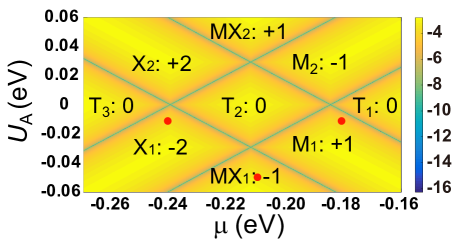
The advantage of our system is that a rich phase diagram for CTSc with different Chern number can be obtained by tuning and . In Fig. 4, we identify the phase diagram in the parameter region eV eV and eV eV. The phase diagram is constructed by tracking the gap at X and M, and dark lines correspond to the gapless points for topological phase transitions. We have carefully checked the band gap in the whole BZ to make sure that gap closing only occurs at X and M in this parameter region. In Fig. 4, the regions labeled by are for trivial phases with Chern number , while the regions with , and () are for CTSc phases with Chern number . We notice that the CTSc phases with the same but opposite carry opposite Chern number . Besides the CTSc phase discussed above, we find another two CTSc phases: and . The energy dispersions for the phase () are shown in Fig. 3c (Fig. 3e) for the bulk and Fig. 3d (3f) for the edge with eV and eV ( eV and eV). Due to the multiple crossings around both X and M, chiral Majorana edge modes and other trivial edge modes coexist at the boundary in these two CTSc phases.
V Discussion and conclusion
The rich phase diagram in Fig. 4 provides us a platform to realize various TSCs junctions for transport experiments. For example, by tuning gate voltage between the phase and the phase, we will be able to construct junction structures with CTSc phase with and the QAH phase (the phase is equivalent to a QAH phase). This type of junction structures will allow us to probe half-integer Hall conductivity Chung et al. (2011) or to realize Majorana interferometry Fu and Kane (2009); Akhmerov et al. (2009). Finally, we emphasize that our strategy can also be generalized to other AFM materials and the key here is to break the symmetry. SC proximity effect has been intensively studied in ferromagnetic materials Buzdin (2005); Bergeret et al. (2005) while anti-ferromagnetism is more compatible with SC. Thus, our work suggests a new avenue to search for CTSc phases.
VI Acknowledgements
X.-Y. Dong acknowledges the support from the Program of Basic Research Development of China (Grant No. 2011CB921901) and National Natural Science Foundation of China (Grant No 11374173). C.-X. Liu acknowledges the support from Office of Naval Research (Grant No. N00014-15-1-2675).
Appendix A Supplementary information for calculation details
Density-functional theory (DFT) calculations were carried out using a plane-wave basis set based on a pseudopotential framework as implemented in the Vienna Ab-initio Simulation Package (VASP)Kresse and Hafner (1993). The exchange-correlation functional was the generalized gradient approximation (GGA) implemented following the Perdew–Burke–Ernzerhof prescriptionPerdew et al. (1996). The missing correlation effect beyond GGA is taken into account through GGAU calculationsAnisimov et al. (1993); Dudarev et al. (1998). Spin-orbit coupling was included for fully relativistic calculations. For the plane-wave calculation, a eV plane-wave cut-off was used. A -point mesh of was used for the integration in the in the Brillouin zone. We adopted the lattice parameters and symmetry (I4/m) of the crystal structure according to the experimental measurement measured at KPaul et al. (2013b, a), for the DFT calculations. In addition of that we use experimental high temperature antiferromagnetic (AFM) configuration (called AF1), as described in the main text for all DFT self-consistent calculations. In previous experimentPaul et al. (2013b, a), two AFM states, referred to as AF1 and AF2, were observed. When cooling down from the room temperature, the compound exhibits a transition from the paramagnetic phase to an AFM phase (i.e. AF1) at 140 K, and a further transition to a new AFM phase (i.e. AF2) at 67 K. Along the axis, an Fe-Os double-layer (DL), in which couples in an FM way between the Fe layer and the Os layer, forms a principle stacking unit. In AF1, the DL couples to other DLs in an FM way along c. In contrast, in AF2 the Fe-Os DLs couple to each other in an AFM way along . Therefore, we adopt a single DL in the thin film model, which is equivalent regarding the bulk AF1 and AF2 phases, as shown in Fig. 1(b) in the main text. To obtain the effective Hamiltonian of this double layer, we performed DFT calculations on the bulk AF1 phase and constructed the thin film model using Wannier functions (see below). Consequently, our thin film model fully considers the material structure, band structure and magnetic properties of ab-initio DFT calculations.
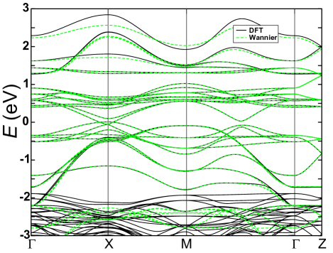
In order to gain insights on the computed electronic structure, we have employed a first-principles based downfolding technique for constructing low energy Hamiltonian. This technique creates few-band, low-energy Hamiltonians from a full DFT Hamiltonians through energy-selective procedure of integrating out degrees of freedom which are not of interest. The effect of the orbitals that are integrated out has been taken into account by renormalization method in the low energy few-band Hamiltonian. If the chosen low-energy bands form an isolated set of bands, the underlying orbitals span the same Hilbert space of the corresponding Wannier functions, giving rise to Wannier functions generated in a direct mannerMostofi et al. (2008). The method provides a first-principles way for deriving a few-band, tight-binding Hamiltonian of the form for a complex system, where the parameters are obtained numerically and define the effective hopping between the active, non-downfolded orbitals, and . () are electron creation (annihilation) operators on site () at orbital (). These downfolding calculations are based on the self-consistent potential and wave functions that obtained from the full ab-initio DFT calculations with all material specific inputs such as experimental crystal structure, chemical information, for example, charge and valence state, hybridization effect between different atoms, magnetic configuration (AF1) and exchange interactions, as well as other information such as the strength of electronic correlation and spin-orbit coupling. For the present case, the effective low-energy Hamiltonian are constructed in Wannier basis of Fe-, Fe- and Os- orbitals only and integrating out all other degrees of freedom. We emphasize that the effect of oxygen orbitals and Sr orbitals is included in a renormalized manner into the few band tight binding Hamiltonian. By including the spin freedom, the low energy Hamiltonian is in the form of matrix (two Fe sites with five orbitals each site, two Os sites and three orbitals each site, and two spins for each orbital). The figure below shows that the band structure obtained by numerically solving the energy selective downfolding Hamiltonian is fully consistent with DFT band structure in the entire Brillouin zone (Fig. S1) and such a consistence ensures that our Wannier function based Hamiltonian correctly mimicking the real dull band structure effect with full material specific information, e.g. band structure, strength of hybridization and exchange interactions, electron-electron correlation, magnetic structure and spin-orbit coupling effect. In particular, although orbitals from oxygen atoms have been integrated out through the procedure described above, their main effect to low energy physics has been included in the exchange coupling between electrons and magnetic moments, which is automatically taken into account in the diagonal term (on-site energy) of our tight-binding Hamiltonian , namely taking different values for opposite spins. Furthermore, we stress that this Hamiltonian does not include any empirical parameters.
Appendix B The effects of CDW/SDW
Above some critical gate voltage , the valence band top at M should be above the conduction band bottom at X (and Y). As a consequence, the electrons will move from to M to X(Y), forming an electron pocket around X(Y) and a hole pocket at M. The scattering between electron Fermi pockets around X and Y may leads to a CDW or SDW in this system. Nevertheless, the topological nature of this system (Berry curvature and Chern number) can not be immediately destroyed by the CDW or SDW since one always needs a band gap closing to induce a topological phase transition can only be induced when there is a (direct) band gap closing. In this section of the supplementary material, we will demonstrate that the main role of CDW/SDW is to split the degeneracy of energy bands at X and Y due to Brillouin zone (BZ) folding. As a consequence, the topological phase transition from Chern number to will be split into two transitions, one from to and the other from to . Therefore, topological phases with non-zero Chern number remains robust for a large gate voltage.
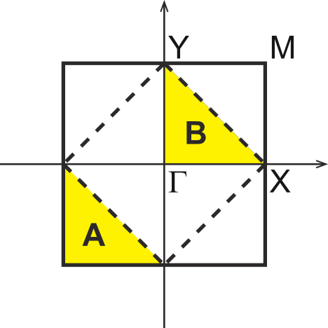
The existence of CDW or SDW will double the unit cell in real space, and the corresponding BZ will be folded. In Fig. S2, the dashed lines enclose the reduced BZ, and the BZ folding process can be exemplified by moving the region A through to region B. In the reduced BZ, the point X and Y are connected by a reciprocal lattice vector and actually the same point.
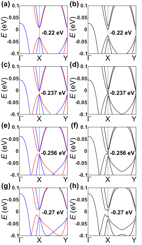
The band structures with different gate voltage are shown in the reduced BZ on -X-Y in Fig. S3. The blue and red lines in the left penal (Fig. S3(a, c, e, g)) are the energy bands without CDW/SDW term, while the black lines in the right penal (Fig. S3(b, d, f, h)) are the energy bands with a small CDW/SDW term. We know that without CDW/SDW term the energy at X and Y point are the same, and in the reduced BZ there will be a double degeneracy at X and Y. As is shown in the main text, the band gap at X (Y) closes when eV, and the Chern number of the system changes from to . When the CDW/SDW term exists, this double degeneracy will be broken and the bonding and anti-bonding states between the electron pockets at X and Y will be formed. In this case, if we tune the gate voltage, two band inversions at X point will happen successively when eV (see Fig. S3(d)) and eV (see Fig. S3(f)). For the gate voltage between and , the Chern number of the system is , since only one band inversion happens. While for (see Fig. S3(h)), two band inversions take place and the Chern number will be +2. Therefore, we have proved that the possible CDW/SDW term will not destroy the scenario of the Dirac physics, and more anomalous Hall phase such as the phase with Chern number could emerge.
Appendix C anomalous Hall phase in a four-layers film
The edge dispersion of a four-layers film in the ribbon configuration is shown in Fig. S4. We add opposite effective electric potential on the top ( eV) and bottom layer ( eV). In the four-layers film the edge modes appears with a smaller asymmetric potential compared to the bilayer case ( eV) in the main text.
Appendix D Effective model around M point
In this section, we will construct the effective model around M point for our system based on symmetry argument. Without external gate voltage and superconducting pairing term, the highest valence band around M point in the BZ is doubly degenerate. We denote the wave function as and . Since the double degeneracy comes from the existence of the symmetry , these two states must be related to each other as . With the help of the numerical calculations, we find
| (12) | |||||
and
| (13) | |||||
which satisfy the relation , and
| (14) |
As a result, on the basis , the matrix representation of is written as
| (17) |
Additional three symmetries, , , and (four-fold rotation symmetry around axis), should be taken into account. Since under the symmetry operations the behaviors of is the same with , we investigate the transformations of the later ones under the symmetry operations.
We choose the reflection plane of and as the plane consisting of and and find
| (18) |
and
| (19) |
With , the matrix form of is given by
| (22) |
At , we have and .
For ,
| (23) |
and
| (24) |
With , we have
| (27) |
leading to and at .
For , we get
| (28) |
and
| (29) |
With , we have
| (32) |
In summary, we have
| (33) | |||
| (34) | |||
| (35) | |||
| (36) |
The transformation properties of the Pauli matrix and are summarized in Tab. S1.
| + | + | + | + | |||
| - | + | - | ||||
| - | - | + | ||||
| + | - | |||||
| + | - | |||||
| - | + | + | + |
When there is no gate voltage, the symmetry exists and the only possible term in the two band effective Hamiltonian is , giving rise to a doubly degenerate parabolic band dispersion around M point in the BZ. For a non-zero gate voltage, the symmetry will be broken and the possible form of the two band Hamiltonian is written as
| (37) | |||||
where and .
Next we will illustrate how the term in the Hamiltonian emerges from the view point of method. Since the term is linear, it should originate from the non-zero term of . According to the form of and , the off-diagonal elements of the effective model could come from the hopping between the Os1 and Os2, such as the term . We need to check the symmetry constraint on these matrix elements. Let’s take the symmetry as an example. We may take the eigen form of the wave functions and operators. For example, the wave functionf transforms with the eigen-value under at M point, the wave function under transforms with the eigen-value and the operator transforms with eigen-value . The combination of these two wave functions and one operator can give rise to identity representation and thus the matrix element is allowed by symmetry (selection rule). Similar procedure can be applied to other matrix elements, leading to the following non-zero matrix elements
| (38) |
where . As a result, can be expressed as
References
- Qi and Zhang (2011) X.-L. Qi and S.-C. Zhang, Rev. Mod. Phys. 83, 1057 (2011).
- Hasan and Kane (2010) M. Z. Hasan and C. L. Kane, Rev. Mod. Phys. 82, 3045 (2010).
- Kitaev (2003) A. Y. Kitaev, Annals of Physics 303, 2 (2003).
- Nayak et al. (2008) C. Nayak, S. H. Simon, A. Stern, M. Freedman, and S. Das Sarma, Rev. Mod. Phys. 80, 1083 (2008).
- Schnyder et al. (2008) A. P. Schnyder, S. Ryu, A. Furusaki, and A. W. Ludwig, Physical Review B 78, 195125 (2008).
- Ryu et al. (2010) S. Ryu, A. P. Schnyder, A. Furusaki, and A. W. Ludwig, New Journal of Physics 12, 065010 (2010).
- Qi et al. (2006) X.-L. Qi, Y.-S. Wu, and S.-C. Zhang, Physical Review B 74, 085308 (2006).
- Yu et al. (2010) R. Yu, W. Zhang, H.-J. Zhang, S.-C. Zhang, X. Dai, and Z. Fang, Science 329, 61 (2010).
- Alicea (2012) J. Alicea, Reports on Progress in Physics 75, 076501 (2012).
- Chang et al. (2013) C.-Z. Chang, J. Zhang, X. Feng, J. Shen, Z. Zhang, M. Guo, K. Li, Y. Ou, P. Wei, L.-L. Wang, et al., Science 340, 167 (2013).
- Chang et al. (2015) C.-Z. Chang, W. Zhao, D. Y. Kim, H. Zhang, B. A. Assaf, D. Heiman, S.-C. Zhang, C. Liu, M. H. Chan, and J. S. Moodera, Nature materials 14, 473 (2015).
- Mackenzie and Maeno (2003) A. P. Mackenzie and Y. Maeno, Rev. Mod. Phys. 75, 657 (2003).
- Mourik et al. (2012) V. Mourik, K. Zuo, S. M. Frolov, S. Plissard, E. Bakkers, and L. Kouwenhoven, Science 336, 1003 (2012).
- Nadj-Perge et al. (2014) S. Nadj-Perge, I. K. Drozdov, J. Li, H. Chen, S. Jeon, J. Seo, A. H. MacDonald, B. A. Bernevig, and A. Yazdani, Science 346, 602 (2014).
- Liang et al. (2013) Q.-F. Liang, L.-H. Wu, and X. Hu, New Journal of Physics 15, 063031 (2013).
- Wu et al. (2015) L.-H. Wu, Q.-F. Liang, and X. Hu, Journal of the Physical Society of Japan 85, 014706 (2015).
- Zhou and Sun (2016) P. Zhou and L. Sun, arXiv preprint arXiv:1601.07705 (2016).
- Qiao et al. (2014) Z. Qiao, W. Ren, H. Chen, L. Bellaiche, Z. Zhang, A. MacDonald, and Q. Niu, Physical review letters 112, 116404 (2014).
- Zhou et al. (2016) J. Zhou, Q.-F. Liang, H. Weng, Y. B. Chen, S.-H. Yao, Y.-F. Chen, J. Dong, and G.-Y. Guo, Phys. Rev. Lett. 116, 256601 (2016).
- Bennemann and Ketterson (2008) K.-H. Bennemann and J. B. Ketterson, Superconductivity: Volume 1: Conventional and Unconventional Superconductors Volume 2: Novel Superconductors (Springer Science & Business Media, 2008).
- Paul et al. (2013a) A. K. Paul, M. Reehuis, V. Ksenofontov, B. Yan, A. Hoser, D. M. Többens, P. M. Abdala, P. Adler, M. Jansen, and C. Felser, Phys. Rev. Lett. 111, 167205 (2013a).
- Paul et al. (2013b) A. K. Paul, M. Jansen, B. Yan, C. Felser, M. Reehuis, and P. M. Abdala, Inorganic chemistry 52, 6713 (2013b).
- Feng et al. (2013) H. L. Feng, Y. Tsujimoto, Y. Guo, Y. Sun, C. I. Sathish, and K. Yamaura, High Pressure Research 33, 221 (2013).
- Kanungo et al. (2014) S. Kanungo, B. Yan, M. Jansen, and C. Felser, Physical Review B 89, 214414 (2014).
- Marzari and Vanderbilt (1997) N. Marzari and D. Vanderbilt, Physical review B 56, 12847 (1997).
- Souza et al. (2001) I. Souza, N. Marzari, and D. Vanderbilt, Physical Review B 65, 035109 (2001).
- Dresselhaus et al. (2007) M. S. Dresselhaus, G. Dresselhaus, and A. Jorio, Group theory: application to the physics of condensed matter (Springer Science & Business Media, 2007).
- Sancho et al. (1985) M. L. Sancho, J. L. Sancho, J. L. Sancho, and J. Rubio, Journal of Physics F: Metal Physics 15, 851 (1985).
- Lee (2009) P. A. Lee, arXiv preprint arXiv:0907.2681 (2009).
- Chung et al. (2011) S. B. Chung, H.-J. Zhang, X.-L. Qi, and S.-C. Zhang, Phys. Rev. B 84, 060510 (2011).
- Qi et al. (2010) X.-L. Qi, T. L. Hughes, and S.-C. Zhang, Phys. Rev. B 82, 184516 (2010).
- Fu and Kane (2009) L. Fu and C. L. Kane, Physical review letters 102, 216403 (2009).
- Akhmerov et al. (2009) A. Akhmerov, J. Nilsson, and C. Beenakker, Physical review letters 102, 216404 (2009).
- Buzdin (2005) A. I. Buzdin, Reviews of modern physics 77, 935 (2005).
- Bergeret et al. (2005) F. Bergeret, A. Volkov, and K. Efetov, Reviews of modern physics 77, 1321 (2005).
- Kresse and Hafner (1993) G. Kresse and J. Hafner, Phys. Rev. B 47, 558 (1993).
- Perdew et al. (1996) J. P. Perdew, K. Burke, and M. Ernzerhof, Phys. Rev. Lett. 77, 3865 (1996).
- Anisimov et al. (1993) V. I. Anisimov, I. V. Solovyev, M. A. Korotin, M. T. Czyżyk, and G. A. Sawatzky, Phys. Rev. B 48, 16929 (1993).
- Dudarev et al. (1998) S. L. Dudarev, G. A. Botton, S. Y. Savrasov, C. J. Humphreys, and A. P. Sutton, Phys. Rev. B 57, 1505 (1998).
- Mostofi et al. (2008) A. A. Mostofi, J. R. Yates, Y.-S. Lee, I. Souza, D. Vanderbilt, and N. Marzari, Computer physics communications 178, 685 (2008).