Low-loss single-mode integrated waveguides in soda-lime glass
Abstract
Low-loss single-mode optical waveguide fabrication process in extra-white soda-lime glass is demonstrated. Waveguiding structures are formed in bulk substrates employing femtosecond laser writing technology. The combination of a slit beam-shaping method and a multiscan fabrication process enables printing of waveguides with a well-defined symmetric cross-section profile. Fabricated waveguides exhibit 0.86 dB/cm propagation loss for 800 nm wavelength. Bending loss in the waveguides are addressed experimentally and compared with a model for radiation loss.
pacs:
42.82.-m, 42.79.Gn, 42.82.BqI Introduction
Recent progress in integrated photonic device fabrication endowed researchers from different branches of optical science with a new versatile toolbox. Optical chips found their application in telecommunication Doerr2015 , biomedical photonics Washburn2011 , quantum optics OBrien2013 , and many other areas. Shrinking complex optical systems onto a single solid-state substrate adds precision and control to the experiment, thus making the integrated platform particularly appealing for the rapidly developing field of photonic technologies.
Femtosecond laser writing (FSLW) of optical waveguides established itself as a low-cost approach for rapid prototyping of unique integrated photonic devices. The widespread availability of femtosecond lasers, both in terms of cost and experience required to handle them, makes the technique advantageous over the more demanding alternative technologies. Moreover, laser writing enables creation of complex 3D photonic structures without resorting to sophisticated multi-step processes, such as those used in lithography. Thus, the FSLW technique is considered a versatile tool.
FSLW enables machining of optical waveguiding structures in virtually any transparent material DellaValle2008 . Single-mode optical waveguide fabrication has been demonstrated in fused silica Shah2005 , borosilicate glasses Eaton2006 , phosphate glasses Chan2003 , chalcogenide glass Efimov2001 , and in a variety of doped glass substrates Schaffer2003 ; Taccheo2004 ; Psaila2007 . Soda-lime glass is an extremely low-cost material, which is commonly used, for example, in base plates for microscopy. It is usually not considered as a good material for demanding optical applications due to a large amount of contained impurities. However, specific material compound allows extra-white soda-lime glass to exhibit very high optical transmission in visible and near-infrared spectral range, thus making the fabrication of integrated optical devices by FSLW feasible as shown in Minoshima2001 ; Kowalevicz2005 ; Tong2006 ; Lazcano2016 .
Laser-written waveguides are formed inside the volume of a moving transparent sample by tightly focused radiation. In order for the radiation intensity to be high enough, pulsed lasers with the pulse duration typically in the picosecond and sub-picosecond range are used, for the relevant nonlinear processes Gattass2008 to leave permanent refractive index change. Several approaches to control the waveguide cross-section are known: shaping the beam and/or the wavefront profile using a cylindrical telescope Osellame2003 , a slit Ams2008 or adaptive optical devices such as a spatial light modulator (SLM) Salter2012 or a deformable mirror simmonds2011 . With such techniques a single scan along the waveguide path can be enough to form a waveguide core in the case of positive refractive index change. However, the process of refractive index change by an intense laser pulse field is an essentially non-equilibrium process that makes the modified volume inhomogeneous. Such inhomogeneities result in additional loss due to scattering and absorption. One can smooth the structure by traversing the laser spot multiple times along the predefined trajectory (multiscan fabrication process), thereby decreasing the loss. Moreover, the cross-section profile of the waveguide can be precisely controlled by means of the multiscan inscription procedure. Multiscan waveguide writing is typically used for fabrication of depressed cladding waveguides (or type-II waveguides) in order to form a waveguide core between several tracks inscribed in the substrate Okhrimchuk2012 . The same principle has been adopted in Nasu2005 ; Psaila2007 ; Bookey2007 ; Brown2012 to print a waveguiding core and more complex structures such as arrayed waveguide gratings Douglass2015 .
In this paper we report an implementation of FSLW technology to form low-loss single-mode optical waveguides in soda-lime glass with the controllable cross-section geometry. Our method employs slit beam shaping and a multiscan processing procedure to fabricate waveguides with a well-defined rectangular cross-section geometry as well as reduced bending and propagation loss. We focus on single-mode waveguides design for 800 nm wavelength, which is convenient for experiments in quantum optics, since both high-quality sources and efficient single-photon detectors (Si APDs) for this wavelength are available. We believe that the results presented here constitute a step towards a cost reduction of chip prototyping and may impact the further development of low-cost integrated photonic components.
II Waveguide fabrication
In FSLW procedure tight laser beam focusing and short pulse length give rise to several nonlinear optical processes inside the focal spot Gattass2008 , which heavily affect the shape and the size of a modified refractive index region. Thus, single scan waveguide writing process may result in a very peculiar core cross-section geometry. For example, one may observe a large thermally-induced low-contrast zone surrounding a guiding core Eaton2008 or even multiple light-guiding regions located in different areas of a treated material sample McMillen2012 . Such specific features of waveguide cross-section can severely limit the topology of integrated optical devices fabricated with FSLW technology. Applications demanding no sophisticated optical circuitry, such as power splitters or waveguide lasers DellaValle2008 , are insensitive to cross-section artifacts if the waveguide has low loss at the desired wavelength, but some recently developed quests in the field of quantum photonics require delicate engineering of complex waveguide arrangement inside the material Crespi2013 . Developing a fabrication process of waveguides with a well-defined cross-section shape and size significantly simplifies further design of complex integrated photonic chips.
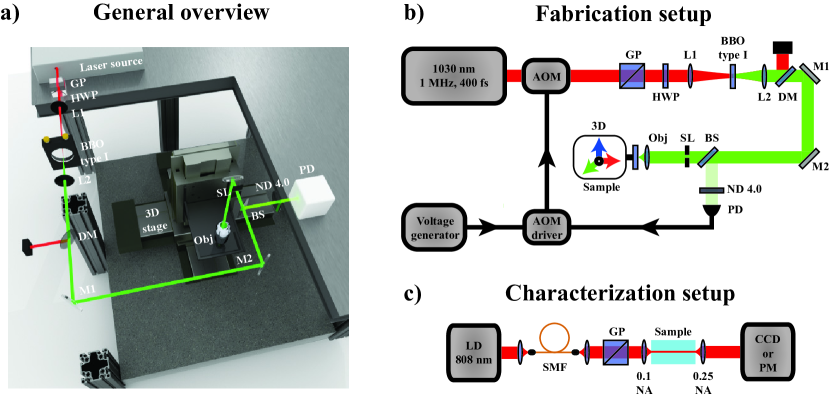
Waveguide fabrication setup used in this work is depicted in Fig. 1. The output of an ytterbium fiber laser (Menlo Systems BlueCut, 400 fs, 1 MHz, 1030 nm) was frequency doubled with a 0.8 mm BBO crystal cut at 23.9°. A small portion of 515 nm laser light was deflected from the main optical path and directed to a photodiode PD. The photodiode tracks the time-varying output power of the laser source and provides a feedback signal for a real-time power stabilization circuit. A slit SL was placed at a distance of approximately 29 cm from the focusing objective. Laser light was focused inside the sample by an infinity corrected 0.7 NA objective with a large working distance (Mitutoyo M Plan Apo 100x). The sample was mounted on a three-axis air-bearing translation stage (AeroTech FiberGlide3D). The power of the writing beam was controlled with an acousto-optic modulator AOM integrated in the laser head. The power stabilization system allowed us to eliminate the detrimental variations in the laser power, stemmed from the instability inherent to the laser itself () and those caused by environmental changes during the writing process, and to ensure the stability of writing conditions over long processing times. A homebuilt external AOM driver circuit with an active feedback loop employed for active power stabilization compared PD output signal and the reference signal from a reference voltage generator and produced the AOM driving voltage. Furthermore, the presented scheme might be used for active tuning of the output power to achieve optimal writing conditions at different fabrication steps. For instance, a combination of an active slit width adjustment and a position-synchronized power modulation may substitute adaptive optic kits in 3D waveguide printing applications demanding additional writing condition correction for different processing depths inside the sample.
Multiscan waveguide printing approach augments the standard FSLW process with an additional degree of freedom, which can be employed for cross-section profile shaping. At first, the FSLW setup has to be tuned to inscribe a uniformly modified refractive index region inside the material in a single scan process. The footprint of a single scan cross-section defines a reasonable range of transverse shifts for the sample translation trajectory in a multiscan process. Our goal was to implement a multiscan waveguide fabrication method to form waveguides with a symmetric and approximately rectangular profile.
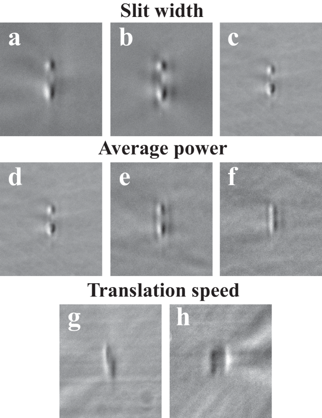
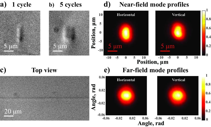
Our initial fabrication setup did not include any beam shaping unit and the Gaussian writing beam was matched with the focusing objective input aperture. In this scheme either uniform but very small modification was induced in a low pulse energy regime or, for larger pulse energies, self-focusing and filamentation nonlinear processes were launched, which were responsible for the formation of an elongated high-contrast core Sudrie2002 surrounded by a large low-contrast halo similar to the one reported in Eaton2008 for N-BK7 glass. We applied a slit beam shaping technique to effectively reduce the numerical aperture of the focusing objective in the direction transverse to the waveguide axis. Even though the fixed slit shaping is not applicable for printing waveguides with a large turning angle Salter2012 it is still the simplest and the most effective beam profile management tool, enabling continuous adjustment of the beam waist in a desired direction. Searching for the optimal single scan process implied sweeping through the slit width, pulse energy and translation speed parameter space, while keeping the desired waveguide printing depth under the surface of the chip constant. Waveguides were printed 175 m below the surface of the sample (Thermo Scientific, ISO 8037/l). Optimal translation speed was determined by visual inspection of uniformity of the inscribed structures. Sample structures for different slit width, pulse energy and translation speed parameters are depicted in Fig. 2, where the pulse energy was measured after the slit. The optimal performance was observed for the following values of the parameters: slit width of 325 m, pulse energy of 42 nJ, and translation speed of 1 mm/s. The optimal translation speed was determined as a trade-off value between minimal longitudinal shear in the multiscan regime and maximal refractive index change. Using these settings we were able to produce uniform structures with elliptical cross-section for a single scan (Fig. 3a). To reduce the eccentricity of the waveguides we performed a multiscan procedure with 1 m transverse shift of each consecutive track producing approximately modified refractive index area (Fig. 3b). A 1 m transverse shift ensured the required overlap between successive modified volumes. End faces of the samples were ground and optically polished after fabrication.
| Polarization | MFDx, m | MFDy, m | Coupling loss | |
|---|---|---|---|---|
| horizontal | 9.20.1 | 12.00.1 | 1.12 dB (12.0 MFD) | |
| vertical | 8.80.1 | 12.40.1 | 1.10 dB (11.2 MFD) |
III Waveguide characterization
III.1 Waveguide fundamental mode profile
Quality of the fabricated waveguides was characterized with a setup shown in Fig. 1(c). The output of a 808 nm diode laser was spatially filtered with a single-mode optical fiber and coupled to a waveguide with a 0.1 NA objective. The sample is mounted on a high-resolution 6-axis mechanical positioner (Luminos I6000). A Glan prism ensures the linear polarization of coupled laser light. Another objective lens with 0.25 NA images the near-field mode profiles on a CCD camera (Fig. 3(d)) with a 36X magnification factor. Far-field profiles (Fig. 3(e)) are captured by the CCD camera after collimating the waveguide output by a 10X objective with f = 18 mm focal length and are used to confirm the single-mode propagation regime.
The measured mode field diameter (MFD) in the near-field allows for a rough estimation of the refractive index contrast induced in the core of the waveguide: the numerical aperture of the waveguide is , where is the refractive index of the bulk material ( for soda-lime glass at the wavelength of interest) and is the wavelength. MFD measurement results and inferred values are summarized in Table 1.
Intrinsic coupling loss arising due to the mode mismatch between the coupled source and the waveguide is estimated by numerically evaluating the mode overlap coefficient of a measured near-field mode profile and the single-mode optical fiber mode profile at 808 nm:
| (1) |
where is the normalized fundamental mode intensity of a single-mode fiber (a typical value of m was taken for a standard Thorlabs SM780HP fiber) and is the normalized measured near-field mode profile of the fabricated waveguide. Peak-to-peak coupling yielded the lowest possible coupling loss coefficient value 2.3 dB for the vertical mode and 2.4 dB for the horizontal mode.
If a free-space coupling scheme is employed, the coupling loss may be minimized by appropriate mode-matching. In this case the loss may be estimated by minimizing the value of given by (1) with respect to the input mode waist . The estimates of coupling loss for a perfectly matched Gaussian beam are provided in Table 1. Similar result may be achieved for a waveguide coupled with a single-mode fiber using a specially designed GRIN lens pigtail.
| Coupling loss | Propagation loss | Bending loss | |
|---|---|---|---|
| This work | 1.10 dB | 0.860.03 dB/cm (808 nm) | 2.7 dB/cm (30 mm radius) |
| Best reported (soda-lime glass) | — | 1.64 dB/cm (800 nm)Kowalevicz2005 | 3 dB/cm (30 mm radius) Tong2006 |
| State-of-the-art (all materials, single-mode at 800 nm) | 0.7 dB (Thorlabs SM800-5.6-125 fiber)Sansoni2010 | 0.5 dB/cm Sansoni2010 | 0.3 dB/cm (30 mm radius)Sansoni2010 |
III.2 Propagation loss
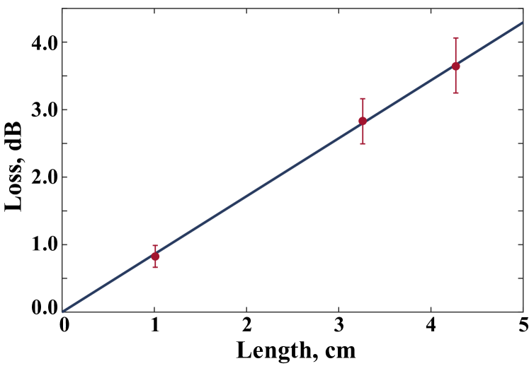
To estimate the propagation loss in straight waveguides we used a cut-back method, assuming that prepared structures are identical and exhibit equal coupling efficiency. However, in practice, the fabrication and post-processing conditions may vary slightly and affect the coupling efficiency and the propagation loss. Thus, to perform a relevant estimation of we printed three chips of different lengths, each containing ten waveguides. Averaging over a series of measurements we evaluated the propagation loss taking into account possible fabrication imperfections. Fig. 4 shows the measurement result. Linear fit of the experimental data gives dB/cm. Good agreement with a linear fitting model indicates that all waveguides exhibit identical average propagation loss, whereas our polishing procedure leaves some residual roughness on the input face of each chip, imposing a constant coupling efficiency uncertainty. The relative uncertainty gradually reduces with increasing length of the chip, indicating the presence of a minor distinction between the different waveguides.
III.3 Bending loss
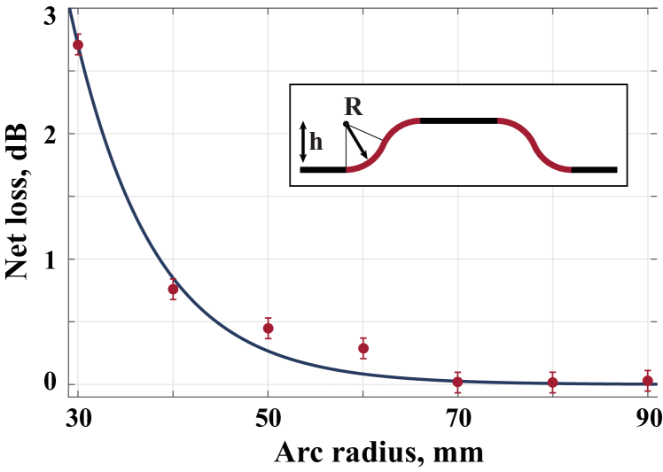
Even primitive integrated photonic devices, such as directional couplers and beam-splitters, require curved waveguides. Bending imposes excess loss due to light propagation in curved sections and mode mismatch effects in joint interfaces. To experimentally quantify bending loss we printed a series of curved waveguides. The inset in Fig. 5 illustrates the geometry of the prepared structures, representing a half of a conventional directional coupler. An array of structures with varying parameters were produced. Each structure in the array consisted of three straight sections and four circular arcs. The radius of arc curvature varied from 30 mm to 90 mm. We measured the overall transmission for each structure. To derive the loss associated solely with bending, we subtract the loss accrued in the straight parts, which were calculated based on the previously obtained results, from the measured overall loss. The resulting bending loss level is shown in Fig. 5 as a function of radius of curvature.
For applications without stringent requirements to minimize photonic circuit footprint, a 70 mm curvature radius should be used due to negligible bending loss ( dB additional net loss). The arc radius may be reduced down to 50 mm imposing additional dB loss if the least possible circuit area is considered.
It is instructive to compare the experimental dependence with an analytical theory for the low-index-contrast case (see, for example, Snyder_Love ). Provided that the mode mismatch in the junction between straight and bent waveguides is negligible, the radiation loss coefficient is given by
| (2) |
where is the radius of curvature, parameter depends on the waveguide cross-section geometry, and
| (3) |
where is the wavenumber, is the refractive index of the bulk, and – the effective mode index of the waveguide. From simple geometrical considerations the total length of the curved part of the waveguide may be calculated as , thereby the losses read:
| (4) |
We fit the bend loss data (Fig. 5) by the exponential dependence (4), which in combination with (3) yields .
As a consistency check we compare the obtained value of with the one derived from the numerical eigenmode simulation for a waveguide having a rectangular cross-section of and a refractive index contrast taken from Table 1. The simulation gives , which is in good agreement with the value obtained from the bending loss analysis.
IV Conclusion
We presented the fabrication process of low-loss single-mode optical waveguides in extra-white soda-lime glass. The waveguide cross-section is shaped to the desired form exploiting a multiscan writing process. With multiscan waveguides we were able to achieve well-defined symmetric mode shapes and reduced propagation and bending loss. We took a detailed account of all types of loss in the waveguides. Importantly, the well defined rectangular shape of the produced waveguides allowed us to quantitatively compare the measured values of bending loss with a simple analytical theory, as well as numerical calculations, and achieve an excellent correspondence.
It would be interesting to compare the properties of our multiscan waveguides with previously reported data for waveguides in soda-lime glass and other optical materials. Such a comparison for an operating wavelength of 800 nm is presented in Table 2. Although the state-of-the-art values obtained with other materials (borosilicate glass) are somewhat better, we have achieved a significant improvement of the waveguides quality in soda-lime glass. Our results may improve the current femtosecond waveguide writing technology extending it to a low-cost material segment.
Authors are grateful to K. S. Kravtsov for enlightening discussions and careful reading of the manuscript, and to N. S. Chupriyanov for considerable help at the early stages of the experiment. This work was supported by the Russian Science Foundation (project 16-12-00017).
References
- (1) C. R. Doerr, Frontiers in Physics 3, 1 (2015).
- (2) A. L. Washburn and R. C. Bailey, The Analyst 136, 227 (2011).
- (3) J. O’Brien, B. Patton, M. Sasaki, and J. Vuckovic, New Journal of Physics 15, 15 (2013).
- (4) G. Della Valle, R. Osellame, and P. Laporta, Journal of Optics A: Pure and Applied Optics 11, 013001 (2008).
- (5) L. Shah, A. Arai, S. Eaton, and P. Herman, Optics express 13, 1999 (2005).
- (6) S. M. Eaton, W.-J. Chen, H. Zhang, and P. R. Herman, Conference on Lasers and Electro-Optics/Quantum Electronics and Laser Science Conference and Photonic Applications Systems Technologies 18, JTuD8 (2006).
- (7) J. W. Chan, T. R. Huser, S. H. Risbud, J. S. Hayden, and D. M. Krol, Applied Physics Letters 82, 2371 (2003).
- (8) O. M. Efimov et al., Optical Materials 17, 379 (2001).
- (9) C. B. Schaffer, J. F. García, and E. Mazur, Applied Physics A: Materials Science and Processing 76, 351 (2003).
- (10) S. Taccheo et al., Optics Letters 29, 2626 (2004).
- (11) N. D. Psaila et al., Conference on Lasers and Electro-Optics, 2007, CLEO 2007 14, 1515 (2007).
- (12) K. Minoshima, a. M. Kowalevicz, I. Hartl, E. P. Ippen, and J. G. Fujimoto, Optics letters 26, 1516 (2001).
- (13) A. M. Kowalevicz, V. Sharma, E. P. Ippen, J. G. Fujimoto, and K. Minoshima, Opt. Lett. 30, 1060 (2005).
- (14) L. Tong, R. R. Gattass, I. Maxwell, J. B. Ashcom, and E. Mazur, Optics Communications 259, 626 (2006).
- (15) H. E. Lazcano and G. V. Vázquez, Appl. Opt. 55, 3268 (2016).
- (16) R. R. Gattass and E. Mazur, Nature Photonics 2, 219 (2008).
- (17) R. Osellame et al., Journal of the Optical Society of America B 20, 1559 (2003).
- (18) M. Ams, G. D. Marshall, P. Dekker, and M. J. Withford, PIERS Online 4, 146 (2008).
- (19) P. S. Salter et al., Optics Letters 37, 470 (2012).
- (20) R. D. Simmonds, P. S. Salter, A. Jesacher, and M. J. Booth, Optics Express 19, 24122 (2011).
- (21) A. Okhrimchuk, V. Mezentsev, A. Shestakov, and I. Bennion, Optics express 20, 3832 (2012).
- (22) Y. Nasu, M. Kohtoku, and Y. Hibino, Opt. Lett. 30, 723 (2005).
- (23) H. T. Bookey, R. R. Thomson, N. D. Psaila, and A. K. Kar, Multi-scan femtosecond laser waveguide inscription in z- cut Lithium Niobate, in CLEO/Pacific Rim, 2007.
- (24) G. Brown, R. R. Thomson, A. K. Kar, N. D. Psaila, and H. T. Bookey, Optics Letters 37, 491 (2012).
- (25) G. Douglass, F. Dreisow, S. Gross, S. Nolte, and M. J. Withford, Optics Express 23, 21392 (2015).
- (26) S. M. Eaton et al., Appl. Opt. 47, 2098 (2008).
- (27) B. McMillen, B. Zhang, K. P. Chen, A. Benayas, and D. Jaque, Opt. Lett. 37, 1418 (2012).
- (28) A. Crespi et al., Nature Photonics 7, 545 (2013).
- (29) L. Sudrie et al., Phys. Rev. Lett. 89, 186601 (2002).
- (30) L. Sansoni et al., Physical Review Letters 105, 1 (2010).
- (31) A. Snyder and J. Love, Optical waveguide theory, Chapman & Hall, 1983.