Spin- and valley-polarized transport across line defects in monolayer MoS2
Abstract
We address the ballistic transmission of charge carriers across ordered line defects in monolayer transition metal dichalcogenides. Our study reveals the presence of a transport gap driven by spin-orbit interactions, spin and valley filtering, both stemming from a simple picture of spin and momentum conservation, as well as the electron-hole asymmetry of charge-carrier transmission. Electronic transport properties of experimentally observed ordered line defects in monolayer , in particular, the vacancy lines and inversion domain boundaries, are further investigated using first-principles Green’s function methodology. Our calculations demonstrate the possibility of achieving nearly complete spin polarization of charge carriers in nanoelectronic devices based on engineered periodic line defects in monolayer transition metal dichalcogenides, thus suggesting a practical scheme for all-electric control of spin transport.
pacs:
73.63.-b, 72.25.-b, 75.70.Tj, 61.72.MmThe spin and valley degrees of freedom of charge carriers are being actively considered as a means of extending the capabilities of present-day charge-based electronics. A major challenge on the way to designing practical devices for generating, manipulating and detecting spin- and valley-polarized charge carriers lies in finding novel physical phenomena and suitable materials that will be utilized in such devices. Two-dimensional (2D) materials such as graphene, and more recently the transition metal dichalcogenides, appear to offer a number of valuable properties for the emerging fields of spintronics Wolf et al. (2001); Žutić et al. (2004); Chappert et al. (2007); Fert (2008) and valleytronics Rycerz et al. (2007); Xiao et al. (2007).
The family of layered transition metal dichalcogenides (TMDs) ( = Mo, W; = S, Se) has attracted considerable attention as prospective materials for next-generation electronics Radisavljevic et al. (2011a, b); Wang et al. (2012) and photovoltaics Bernardi et al. (2013). Single layers of the -phase TMDs are direct band gap semiconductors with valence and conduction bands located at the inequivalent and points of the Brillouin zone [see Fig. 1(a) for a schematic illustration of the band structure] Splendiani et al. (2010); Mak et al. (2010); Jin et al. (2013); Zhang et al. (2014). Single-layer TMDs lack inversion symmetry, hence a spin-orbit interaction lifts the spin degeneracy of the bands. The effect of a spin-orbit interaction is particularly pronounced in the valence band, giving rise to spin splittings of 0.15–0.46 eV across the family of single-layer TMDs Zhu et al. (2011). A combination of the two properties mentioned above results in an intrinsic spin-valley coupling of the hole charge carriers Xiao et al. (2012), thus making these materials an appealing choice for beyond-electronics applications. However, the potential of this novel physical phenomenon for prospective technological applications is far from being fully explored. While valley polarization of charge carriers by optical means has been recently reported Zeng et al. (2012); Mak et al. (2012); Cao et al. (2012), neither practical all-electric schemes for generating polarized charge carriers nor spin transport phenomena in monolayer TMDs have been demonstrated so far.

In this Rapid Communication, we propose a simple approach for generating spin- and valley-polarized charge carriers by means of transmission across periodic line defects in monolayer TMDs. Our study also reveals a number of transport phenomena in these materials, such as the suppression of hole transmission across inversion domain boundaries driven by spin-orbit splitting of the valence band. Our predictions, which are based on a simple and intuitive picture of spin and momentum conservation, are further supported by the results of first-principles Green’s function calculations, which reveal the quantitative aspects of spin- and valley-polarized transport across representative line defects in monolayer that have been observed experimentally and can be engineered in a controlled manner.
We will first discuss the general phenomenology without making recourse to any particular member of the family of TMD materials or to a specific defect structure. It is, however, worth stressing that line defects in TMDs, such as grain boundaries and inversion domain boundaries (equivalent to grain boundaries), tend to exhibit well-ordered periodic structures Zhou et al. (2013); van der Zande et al. (2013); Najmaei et al. (2013); Yazyev and Chen (2014). The periodicity vector of a one-dimensional defect is defined by the commensurability condition, that is, by matching two translational vectors in the “left” and “right” domains separated by the defect Yazyev and Louie (2010)
| (1) |
where (, ) and (, ) are the lattice vectors of the “left” and “right” domains, respectively, and , are pairs of integers.
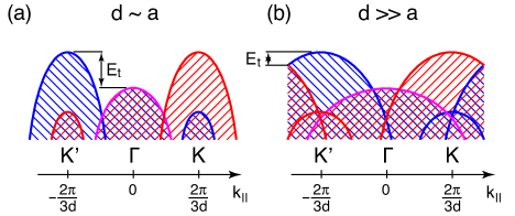
Figure 1(b) shows the band structure of a monolayer TMD projected onto the direction of momentum parallel to the defect, , when this defect is oriented along one of the lattice vectors [or, more generally, when ]. In this situation, which is most often observed in experiments, the two valleys at points () and () of the Brillouin zone are separated in . Once is conserved upon transmission, two possibilities can be realized. For defects characterized by
| (2) |
such as the structures that do not change lattice orientation [e.g., ], valley indices are conserved upon transmission. Figure 1(c) shows the allowed transport channels for hole charge carries when spin is additionally conserved upon transmission across such periodic defects. In this situation, spin and momentum conservation does not lead to transmission blocking at any charge-carrier concentration.
Figure 1(d) illustrates a different situation defined by
| (3) |
in which the valley indices are exchanged upon crossing the defect. This scenario is realized in inversion domain boundary defects, which can be defined by the lattice vectors and , and thus and , in order to satisfy the commensurability condition (1). At low concentrations of hole charge carriers, this will result in a complete suppression of transmission if both spin and momentum are conserved. At larger charge-carrier concentrations, additional allowed channels will be involved once the opposite-spin branches separated by spin splitting start being populated. In order to complete the picture of ballistic transmission across the inversion domain boundary defects, one needs to consider two more contributions: (i) transmission of the hole charge carriers populating the spin-degenerate valley at the point, which is separated from the valence band maximum by relatively small energies [see Fig. 1(b)], and (ii) the overlap of the and valleys along at larger , as illustrated in Fig. 2. Overall, one can expect a strong suppression of the transmission of hole charge carriers across the inversion domain boundaries, with the magnitude of the effective transport gap defined by
| (4) |
where is the characteristic energy of the valence band with an effective charge-carrier mass , and is the lattice constant.
The fact that the two valleys are separated in in the considered scenarios will result in discrimination of the transmitted charge carriers with respect to their valley index and incidence angle . This effect was originally predicted Gunlycke and White (2011) for a particular experimentally observed line defect in graphene Lahiri et al. (2010); Chen et al. (2014). We argue, however, that valley filtering is expected for any periodic line defect which leaves the two valleys separated in space since the following property holds for valley-resolved transmissions,
| (5) |
for the incidence angle bijectively related to momentum in the one-dimensional (1D) Brillouin zone of the defect. The corresponding valley polarization of the transmitted charge
| (6) |
is generally nonzero for any . At low concentrations, the valley polarization of hole charge carriers is equivalent to their spin polarization , due to the intrinsic spin-valley coupling in monolayer TMDs Xiao et al. (2012). The latter property, however, is different as spin is an intrinsic property of an electron, hence spin-polarized charge carriers can be injected into other materials. The considered defects can thus be used for controlling the spin polarization of charge carriers by all-electric means without the use of magnetic materials.
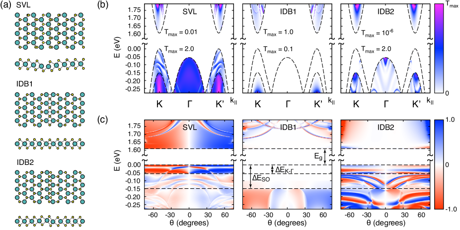
In order to investigate the quantitative aspects of the predicted spin- and valley-polarized transport phenomena, we perform first-principles quantum transport simulations using the Green’s function technique with spin-orbit interactions accounted for by using two-component spinor wave functions in combination with fully relativistic norm-conserving pseudopotentials (for a detailed description, see the Supplemental Material methodology ). Without loss of generality, we further focus our attention on monolayer as a representative member of the monolayer TMD materials family. In our density functional theory calculations, we obtain eV for the band gap. The calculated band offset between the and valence bands eV, while the spin splitting of the valence bands at points eV, both in agreement with experiments and previous calculations Jin et al. (2013); Zhu et al. (2011). The effective mass of hole charge carriers corresponds to the characteristic energy eV. As an example of a periodic line defect realizing the situation shown in Fig. 1(c), we consider the single vacancy line (SVL) defects reported by Komsa et al. Komsa et al. (2013). Two different structures of inversion domain boundaries (IDB1 and IDB2), observed in Refs. Zhou et al., 2013; Lin et al., 2014; Lehtinen et al., 2015; Lin et al., 2015, were considered as examples of systems realizing the second transport scenario shown in Fig. 1(d). All three defect structures are oriented along one of the lattice vectors (often referred to as the zigzag direction) and have the smallest possible periodicity . Importantly, the above-mentioned ordered defects can be engineered with a fair degree of control at transmission electron microscopy conditions Komsa et al. (2013); Lin et al. (2014); Lehtinen et al. (2015); Lin et al. (2015). The atomic structures of these line defects are shown in Fig. 3(a).
Figure 3(b) shows the calculated charge-carrier transmissions , across the investigated line defects in , as a function of energy relative to the valence band maximum and momentum parallel to the defect. One can immediately notice the predicted suppression of transmission across the inversion domain boundaries (IDB1 and IDB2) for the low-energy hole charge carriers. In monolayer , the transport gap is governed by the band offset rather than the spin splitting of the valley bands, that is, [cf. Eq. (4)]. In the case of the IDB1 defect, the transmission is strictly zero for , while for the IDB2 structure a residual transmission not exceeding 10-3 was found within the predicted transport gap. The latter is enabled by the spin-flip process due to out-of-plane bending at the defect line [Fig. 3(a)]. In general, shows strong variations in both and , with linelike suppression typical of resonant backscattering on localized states hosted by the defects Zou et al. (2013); Zhou et al. (2013). A similar phenomenon was also reported for the charge-carrier transmission across a line defect in graphene Chen et al. (2014).
Figure 3(c) shows the calculated spin polarization of transmitted charge carriers as a function of their energy and incidence angle . The most prominent spin polarization is found for the SVL defect at energies where the hole charge carriers belong only to fully spin-polarized valleys and . For instance, at meV, spin polarization achieves at incidence angles . Importantly, at these charge-carrier energies the transmissions are also high, of the order of 1. This combination of properties identifies the optimal conditions for using ordered vacancy line defects in nanoscale spintronic devices. At the spin polarization dramatically reduces due to a large contribution to conductance of charge carriers in the spin-degenerate valley, which is also characterized by large transmissions. Interestingly, large values of are also found for the electron charge carriers, although spin-orbit effects in the conduction band are generally weaker and have a complex character. In this case, transmissions are found to be about two orders of magnitude lower.
For the IDB1 defect we generally find a lower degree of across the relevant range of values of and . The dominant contribution to the transmission of holes comes from conductance channels involving and valleys, as indicated in Fig. 1(d). A sharp decrease of spin polarization within is due to the fact that only one of the two indicated channels is realized in this range of incidence angle values Habe and Koshino (2015). Specifically, transmission to the topmost valence band without a spin flip in this region is prohibited. The degree of spin polarization of holes transmitted across IDB2 shows large variations with respect to energy and angle , even in the energy range which corresponds to residual transmission enabled by the spin-flip process. The sign of at a constant incidence angle changes at meV. For multiple conductance channels compete, resulting in an irregular behavior of spin polarization.
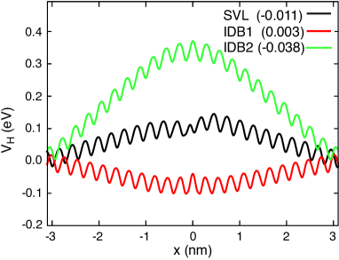
It is interesting to note the pronounced electron-hole asymmetry of the ballistic conductances in all three considered cases [Fig. 3(b)]. The calculated transmissions of the hole charge carrier across the SVL and IDB2 line defects tend to approach their maximum nominal value of 2, which is the largest number of transmission channels within the investigated energy range. In contrast, the transmission of electron charge carriers is greatly suppressed across both defects. The opposite is true for the IDB1 line defect – the transmission of low-energy electron charge carriers is generally higher, which was also predicted for the same defect structure in MoSe2 Lehtinen et al. (2015). We explain this behavior from the point of view of electrostatic potential bending at the defect, which can be quantified in terms of the self-consistent Hartree potential within the scattering region obtained from our first-principles calculations (Fig. 4). For both the SVL and IDB2 line defects we observe upward potential bending which leads to a tunnelinglike transmission of electrons (hence their lower transmission), but not holes. Moreover, the larger height of the potential barrier in the case of IDB2 is reflected in lower transmissions of low-energy electrons in comparison with the SVL defect. The reversed behavior of charge carriers crossing the IDB1 defect is related to the downward potential bending. The sign and magnitude of potential bending is defined by an effective charge localized on the defect (cf. Fig. 4), and a competing contribution due to the head-to-head change of polarization taking place upon crossing the IDB1 and IDB2 defects, as shown in the inset to Fig. 1(d). A similar polarization discontinuity has recently been predicted to occur at the interfaces created upon selective functionalization of 2D materials Gibertini14 . The contribution of polarization discontinuity dominates in the case of the IDB1 structure, thus leading to a downward potential bending, while the effective large negative charge in the case of the IDB2 defect results in an upward potential bending.
In conclusion, our work reveals a number of transport phenomena in the transmission of charge carriers across ordered line defects in monolayer stemming from a simple and intuitive picture of spin and momentum conservation combined with strong spin-orbit effects in this two-dimensional material. The results are valid for other members of the monolayer TMD family of materials, but one can also expect such phenomena to be observed in other semiconductors featuring strong spin-orbit interactions. Our work constitutes an important step towards understanding the transport properties of realistic samples of monolayer TMDs. Furthermore, we believe it also opens an avenue towards conceptually different nanoscale devices for electronics, and their extensions, such as spintronics and valleytronics. The energy of the charge carriers in such devices operated in the ballistic regime can be controlled by means of gating, while the angle dependence can be harnessed by positioning local contacts in predefined configurations relative to the line defect Yu11 ; Tsen12 ; Lee15 . For the purpose of confirming the predicted filtering phenomenon, coupled spin and valley polarizations of the charge carriers can be detected using ferromagnetic contacts or by optical means Zeng et al. (2012); Mak et al. (2012); Shan15 . For instance, one can perform spatially resolved measurements of the circular polarization of light emitted upon electroluminescence Ross14 in devices containing line defects. Practical devices relying on all-electric schemes could rather use components in the valve configuration, as suggested for a graphene-based valleytronic device Chen et al. (2014). Considering the recently demonstrated long lifetimes of spin-polarized charge carriers in monolayer TMDs Yang15 , our work opens an avenue towards developing practical schemes for achieving all-electric control of spin transport in spintronic devices.
We thank G. Autès, F. Gargiulo, and A. Kis for discussions. This work was supported by the Swiss NSF (Grant No. PP00P2_133552) and the ERC Starting grant “TopoMat” (Grant No. 306504). First-principles calculations have been performed at the Swiss National Supercomputing Centre (CSCS) under project s515.
References
- Wolf et al. (2001) S. A. Wolf, D. D. Awschalom, R. A. Buhrman, J. M. Daughton, S. von Molnár, M. L. Roukes, A. Y. Chtchelkanova, and D. M. Treger, Science 294, 1488 (2001).
- Žutić et al. (2004) I. Žutić, J. Fabian, and S. Das Sarma, Rev. Mod. Phys. 76, 323 (2004).
- Chappert et al. (2007) C. Chappert, A. Fert, and F. N. Van Dau, Nature Mater. 6, 813 (2007).
- Fert (2008) A. Fert, Rev. Mod. Phys. 80, 1517 (2008).
- Rycerz et al. (2007) A. Rycerz, J. Tworzydło, and C. W. J. Beenakker, Nature Phys. 3, 172 (2007).
- Xiao et al. (2007) D. Xiao, W. Yao, and Q. Niu, Phys. Rev. Lett. 99, 236809 (2007).
- Radisavljevic et al. (2011a) B. Radisavljevic, A. Radenovic, J. Brivio, V. Giacometti, and A. Kis, Nature Nanotechnol. 6, 147 (2011a).
- Radisavljevic et al. (2011b) B. Radisavljevic, M. B. Whitwick, and A. Kis, ACS Nano 5, 9934 (2011b).
- Wang et al. (2012) Q. H. Wang, K. Kalantar-Zadeh, A. Kis, J. N. Coleman, and M. S. Strano, Nature Nanotechnol. 7, 699 (2012).
- Bernardi et al. (2013) M. Bernardi, M. Palummo, and J. C. Grossman, Nano Lett. 13, 3664 (2013).
- Splendiani et al. (2010) A. Splendiani, L. Sun, Y. Zhang, T. Li, J. Kim, C.-Y. Chim, G. Galli, and F. Wang, Nano Lett. 10, 1271 (2010).
- Mak et al. (2010) K. F. Mak, C. Lee, J. Hone, J. Shan, and T. F. Heinz, Phys. Rev. Lett. 105, 136805 (2010).
- Jin et al. (2013) W. Jin, P.-C. Yeh, N. Zaki, D. Zhang, J. T. Sadowski, A. Al-Mahboob, A. M. van der Zande, D. A. Chenet, J. I. Dadap, I. P. Herman, et al., Phys. Rev. Lett. 111, 106801 (2013).
- Zhang et al. (2014) Y. Zhang, T.-R. Chang, B. Zhou, Y.-T. Cui, H. Yan, Z. Liu, F. Schmitt, J. Lee, R. Moore, Y. Chen, et al., Nature Nanotechnol. 9, 111 (2014).
- Zhu et al. (2011) Z. Zhu, Y. Cheng, and U. Schwingenschlögl, Phys. Rev. B 84, 153402 (2011).
- Xiao et al. (2012) D. Xiao, G.-B. Liu, W. Feng, X. Xu, and W. Yao, Phys. Rev. Lett. 108, 196802 (2012).
- Zeng et al. (2012) H. Zeng, J. Dai, W. Yao, D. Xiao, and X. Cui, Nature Nanotechnol. 7, 490 (2012).
- Mak et al. (2012) K. F. Mak, K. He, J. Shan, and T. F. Heinz, Nature Nanotechnol. 7, 494 (2012).
- Cao et al. (2012) T. Cao, G. Wang, W. Han, H. Ye, C. Zhu, J. Shi, Q. Niu, P. Tan, E. Wang, B. Liu, et al., Nature Commun. 3, 887 (2012).
- Zhou et al. (2013) W. Zhou, X. Zou, S. Najmaei, Z. Liu, Y. Shi, J. Kong, J. Lou, P. M. Ajayan, B. I. Yakobson, and J.-C. Idrobo, Nano Lett. 13, 2615 (2013).
- van der Zande et al. (2013) A. M. van der Zande, P. Y. Huang, D. A. Chenet, T. C. Berkelbach, Y. You, G.-H. Lee, T. F. Heinz, D. R. Reichman, D. A. Muller, and J. C. Hone, Nature Mater. 12, 554 (2013).
- Najmaei et al. (2013) S. Najmaei, Z. Liu, W. Zhou, X. Zou, G. Shi, S. Lei, B. I. Yakobson, J.-C. Idrobo, P. M. Ajayan, and J. Lou, Nature Mater. 12, 754 (2013).
- Yazyev and Chen (2014) O. V. Yazyev and Y. P. Chen, Nature Nanotechnol. 9, 755 (2014).
- Yazyev and Louie (2010) O. V. Yazyev and S. G. Louie, Nature Mater. 9, 806 (2010).
- Komsa et al. (2013) H.-P. Komsa, S. Kurasch, O. Lehtinen, U. Kaiser, and A. V. Krasheninnikov, Phys. Rev. B 88, 035301 (2013).
- Lin et al. (2014) Y.-C. Lin, D. O. Dumcenco, Y.-S. Huang, and K. Suenaga, Nature Nanotechnol. 9, 391 (2014).
- Lehtinen et al. (2015) O. Lehtinen, H.-P. Komsa, A. Pulkin, M. B. Whitwick, M.-W. Chen, T. Lehnert, M. J. Mohn, O. V. Yazyev, A. Kis, U. Kaiser, et al., ACS Nano 9, 3274 (2015).
- Lin et al. (2015) J. Lin, S. T. Pantelides, and W. Zhou, ACS Nano 9, 5189 (2015).
- Gunlycke and White (2011) D. Gunlycke and C. T. White, Phys. Rev. Lett. 106, 136806 (2011).
- Lahiri et al. (2010) J. Lahiri, Y. Lin, P. Bozkurt, I. I. Oleynik, and M. Batzill, Nature Nanotechnol. 5, 326 (2010).
- Chen et al. (2014) J. H. Chen, G. Autès, N. Alem, F. Gargiulo, A. Gautam, M. Linck, C. Kisielowski, O. V. Yazyev, S. G. Louie, and A. Zettl, Phys. Rev. B 89, 121407 (2014).
- Zou et al. (2013) X. Zou, Y. Liu, and B. I. Yakobson, Nano Lett. 13, 253 (2013).
- Habe and Koshino (2015) T. Habe and M. Koshino, Phys. Rev. B 91, 201407 (2015).
- (34) See Supplemental Material at http://link.aps.org/supplemental/… for the detailed description of computational methodology.
- (35) M. Gibertini, G. Pizzi, and N. Marzari, Nature Commun. 5, 5157 (2014).
- (36) Q. Yu, L. A. Jauregui, W. Wu, R. Colby, J. Tian, Z. Su, H. Cao, Z. Liu, D. Pandey, D. Wei, T. F. Chung, P. Peng, N. P. Guisinger, E. A. Stach, J. Bao, S.-S. Pei, and Y. P. Chen, Nature Mater. 10, 443 (2011).
- (37) A. W. Tsen, L. Brown, M. P. Levendorf, F. Ghahari, P. Y. Huang, R. W. Havener, C. S. Ruiz-Vargas, D. A. Muller, P. Kim, and J. Park, Science 336, 1143 (2012).
- (38) G.-H. Lee, G.-H. Park, and H.-J. Lee, Nature Phys., doi:10.1038/nphys3460 (2015).
- (39) W.-Y. Shan, J. Zhou, and D. Xiao, Phys. Rev. B 91, 035402 (2015).
- (40) J. S. Ross, P. Klement, A. M. Jones, N. J. Ghimire, J. Yan, D. G. Mandrus, T. Taniguchi, K. Watanabe, K. Kitamura, W. Yao, D. H. Cobden, and X. Xu, Nature Nanotechnol. 9, 268 (2014).
- (41) L. Yang, N. A. Sinitsyn, W. Chen, J. Yuan, J. Zhang, J. Lou, and S. A. Crooker, Nature Phys. 11, 830 (2015).