Investigations of temperature-dependent photoluminescence of uncoated and silver-coated CdS quantum dots
Abstract
We report temperature-dependent photoluminescence (PL) studies and PL relaxation dynamics for uncoated and silver-coated CdS quantum dots (QDs). Room-temperature photoluminescence studies indicate that the presence of silver coating on CdS QD samples enhances the blue luminescence corresponding to the band-to-band transitions by a factor of ten compared to the uncoated samples. Furthermore, the decay time measurements using Time Correlated Single Photon Counting technique demonstrate Förster resonance energy transfer (FRET) between silver-shell and CdS-core in silver-coated CdS QD samples. A detailed investigation of temperature-dependent PL spectra of uncoated CdS QD samples reveals the role of thermally-activated surface-trap states, exciton-LO phonon coupling and ionized impurity scattering. In case of silver-coated QDs, the temperature-dependent PL peak energy corresponding to the band-to-band transitions presents a consecutive red-blue-red shift (S-shaped) behavior. Whereas, the full width at half maximum (FWHM) shows a successive blue-red-blue shift (inverted S-shaped) characteristic with increasing temperature.
pacs:
78.66.Qn, 78.67.Bf, 78.47.ϩp, 78.55.EtI Introduction
Semiconductor quantum dots (SQDs) due to their size-tunable energy band-gap and large oscillator strength have become extensively lucrative for light-emitting diodes (LEDs) Sun et al. (2012); Son et al. (2012), photovoltaic cells Huynh et al. (2002), optically pumped lasers Klimov et al. (2000); Duan et al. (2003), telecommunications Harrison et al. (2009) and in biological labels Bruchez et al. (1998). Coupling of surface plasmon and QD resonances can open new avenues to further modify their spectral characteristics favorably Pompa et al. (2006). An interplay between plasmonic resonance and the inter-band electronic transitions in the SQDs can modify oscillator strength, energy level, PL peak positions and width, and relaxation dynamics. In this regard, silver-coated CdS QDs are of special interest because CdS quantum dots have high-photoluminescence quantum yield. Also, among all metals, silver exhibits the most pronounced Mie resonance Kalyaniwalla et al. (1990). It is thus important to develop new methods of synthesis and characterization of metal-coated SQDs. Mostafavi et al. reported gamma irradiation method to synthesize highly-monodispersed alloyed QDs Mostafavi et al. (2000). In addition to synthesis and characterization, an in-depth knowledge of the radiative and nonradiative relaxation processes in these silver-coated and uncoated SQDs is not only intriguing for fundamental physics, but also relevant for future applications in photonics and optoelectronic devices.
Until now, temperature-dependent photoluminescence (TDPL) have been studied for a wide variety of SQD samples Valerini et al. (2005); Hsu et al. (2007). However, to the best of our knowledge, there are hardly any such studies in semiconductor / metal core-shell QDs. In this paper, we report a detailed investigation of structural determination, optical absorption and TDPL studies of such uncoated and silver-coated CdS QDs. We find that silver coating on CdS QDs enhances the band-to-band luminescence significantly and correspondingly suppresses surface / defect state luminescence. A detailed study of the temperature dependence of the PL spectra of uncoated and Ag-coated CdS QDs is shown to reveal the role of thermally activated surface-trap states. We also demonstrate that the main nonradiative processes are thermal escape of carriers assisted by LO phonons and thermally activated ionized impurity scattering.
II Experimental
For the preparation of CdS nanoparticles, 100 ml of M cadmium sulphate () solution and 100 ml of M 2-mercaptoethanol () were added to sodium phosphate buffer solution (). Thereafter, a -ray source with 2.65 dose rate was used to irradiate the resultant solution. All the reagents are of analytical grade (Sigma-Aldrich) and are used without further purification. Mili-Q water (18 M cm-1) was used to prepare solutions. Since the growth of clusters is highly dependent on any type of nuclei, the vessels were cleaned with concentrated solution in order to remove all contaminations. The solutions were isolated from air and then de-aerated by bubbling nitrogen. The steady state irradiation of the solution results in the continuous release of radical species. Finally CdS molecules are formed through the reaction,
| (1) |
Consequently, CdS molecules coalesce to form CdS clusters in solution. Eight samples were prepared varying the dose of gamma irradiation from 0.2 kGy to 7.5 kGy. These samples are named as CdS1, CdS2 and so on. All samples are tested for any residual radioactivity and are used for further experiments only when they were found free of any radioactivity.
II.1 Deposition of Silver on CdS Nanoparticles
Silver was deposited on two CdS QD samples namely CdS2 and CdS8 which
were synthesized with 0.3 and 7.5 kGy dose.
These two samples after depositing silver are named as CdS2@Ag and CdS8@Ag respectively.
The deposition of silver on CdS nanoparticles was done in three steps.
First, excess of ionic compounds were removed from CdS
solution by amberlite treatment and then 10 ml of 0.5 gm wt
polyvinyl sulfate polymer (PVS) was added to avoid
the coalescence of the CdS nano particles.
Second, 5 ml of M silver nitrate
solution was slowly injected under rigorous stirring.
5 ml of M formaldehyde was added to the CdS solution.
Formaldehyde was used as the reducing agent.
When silver ions are reduced by formaldehyde
in presence of CdS particles, the reduction occurs
instantaneously and individual (Ag)n particles are
not produced Frederic et al. (2004).
For structural characterization, high-resolution
transmission electron microscopy (HRTEM) was used.
Spectroscopic studies such as UV-Vis absorption and
PL were performed on these colloidal solution of uncoated
and silver-coated CdS QD samples.
Temperature-dependent PL spectroscopy was done on
solid thin films prepared by spin coating technique.
Clean silicon wafers were used as substrates as they do not luminesce.
A closed cycle He refrigerator was used for cooling
the sample to 10 K. He-Cd laser (wavelength: 325 nm)
of power 25 mW was used as the excitation source.
PL spectra were recorded using a spectrometer with
CCD camera, cooled to 210 K.
III Results and Discussion
III.1 Structural characterization
Representative high-resolution transmission electron microscopy (HRTEM) images of uncoated CdS QDs (CdS2) are shown in Fig. 1 (a).
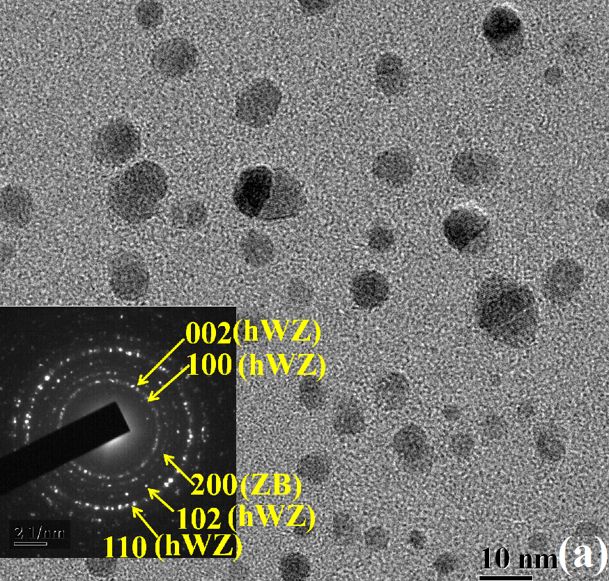
The inset shows the selected area electron diffraction (SAED) of the QDs. The lattice spacing () between adjacent (hkl) lattice planes are obtained from the diameter of the diffraction rings. Deploying these values, lattice parameters a and c are obtained. Comparing these values with literature values for hexagonal-wurtzite (hWZ) and cubic zinc-blende (ZB) crystal structures, we deduce information about the crystal structure of these QDs (see Table 1).
| Avg. radius | Crystal | |||||
|---|---|---|---|---|---|---|
| (nm-1) | () | Literature value () | type | |||
| 2.810 | 3.559 | 3.5688 [PDF 80-0006] | 1 | 0 | 0 | hexagonal |
| 3.005 | 3.333 | 3.3410 [PDF 80-0006] | 0 | 0 | 2 | hexagonal |
| 3.448 | 2.900 | 2.9055 [PDF 80-0019] | 2 | 0 | 0 | cubic |
| 4.121 | 2.430 | 2.4390 [PDF 80-0006] | 1 | 0 | 2 | hexagonal |
| 4.906 | 2.038 | 2.0605 [PDF 80-0006] | 1 | 1 | 0 | hexagonal |
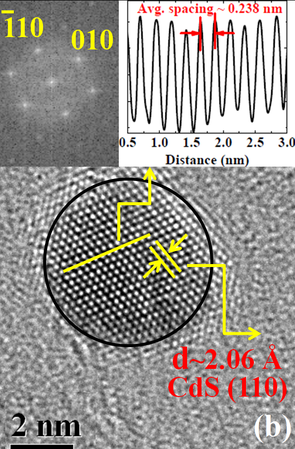
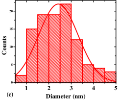
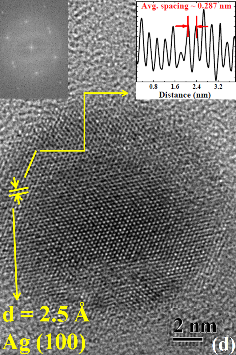
In conclusion, the analysis of SAED image indicates the presence of planes corresponding to hexagonal-wurtzite (hWZ) and cubic zinc-blende (ZB) crystal structures in case of these CdS QDs. It has already been reported for CdS QDs, in 4-6 nm range, that the crystal structure phase changes from bulk hexagonal-wurtzite type to cubic zinc-blende structure Banerjee et al. (2000). The crystal structure has been found to be exclusively dependent on the size of the QD. For QDs with diameter less than 4 nm, the crystal structure has been reported to be cubic zinc-blende structure; whereas that with diameter greater than 6 nm, the structure has been reported to be hexagonal-wurtzite structure. For the QDs with diameter in the range of 4-6 nm, both the cubic and hexagonal phase co-exist sharing their close-packed planes at the boundary Ricolleau et al. (1998). Fig. 1 (b) and (c) show the HRTEM images of individual CdS QDs of diameter 5 nm and 3 nm respectively. The HRTEM lattice image of individual CdS QDs show the well-spaced lattice fringes indicating a single crystal structure of CdS QDs with high crystalline quality. The left side inset shows the FFT of the circled region and the right side inset shows the average lattice point spacing. This lattice point spacing (L) makes an angle with the lattice plane spacing (). Therefore, the lattice plane spacing is obtained using the relation: . The crystal plane spacing comes out to be 2.06 , which correspond to crystal plane spacing of CdS (220) zinc-blende single crystal or CdS (110) of hexagonal-wurtzite single crystal. Fig. 1 (d) shows an individual silver-coated QD. A close look at this image reveals that each particle consist of a darker center part compared to the edge. This color contrast is attributed to the silver-coating on CdS QDs. The left side inset shows the FFT of this Silver-coated CdS QDs. The right side inset shows the average lattice point spacing. The crystal plane spacing comes out to be 2.5 , which correspond to crystal plane spacing of Ag (100) hexagonal-wurtzite single crystal [PDF 87-0598].
III.2 Absorption spectroscopy
A LAMBDA 950 UV/Vis/NIR spectrophotometer (PerkinElmer) is used to record absorption spectra of the CdS QD samples. The UV-Vis absorption spectra of colloidal solutions, before and after -irradiation with different doses, are shown in Fig. 2 (a).
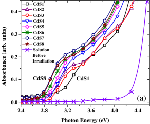
The absorption spectra are obtained towards analyzing the quantum-size effect of the CdS nanoparticles. The peak positions of the absorption bands for these SQD samples appear in the range 2.9 eV to 3.3 eV. While, the band-gap of bulk CdS is 2.42 eV. This large blue shift of the band edge is due to strong quantum confinement effect in the smaller CdS QDs of radius less than exciton Bohr-radius (= 2.8 nm for CdS Gaponenko (1998)). In case of lower doses (0.2 kGy - 0.4 kGy), we observe multiple absorption peaks which appear due to overlap of higher-order excited states corresponding to different particle size QDs. The corresponding band gap for each sample is determined from the position of the excitonic absorption feature. Further, the size of QDs are obtained from data reported in Nair Nair et al. (1992), where they calculate the QD diameter numerically using conduction-valence-band model (CVBM) for CdS QD. Measured band gap and average QD diameter for different samples corresponding to different -irradiation dose are shown in Table 2.
| Sample | Dose | Bandgap | Diameter |
| (kGy) | (eV) | (nm) | |
| CdS1 | 0.2 | 3.25 | 3.3 |
| CdS2 | 0.3 | 3.07 | 4.2 |
| CdS3 | 0.4 | 3.05 | 4.0 |
| CdS4 | 1.5 | 3.05 | 4.2 |
| CdS5 | 3.0 | 3.02 | 4.4 |
| CdS6 | 4.5 | 2.95 | 4.8 |
| CdS7 | 6.4 | 2.90 | 5.5 |
| CdS8 | 7.5 | 2.90 | 5.5 |
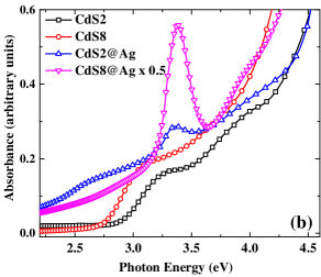
The calculated particle size values are in good agreement with the HRTEM results. With increasing dose, the spectra shift towards red, which suggests the formation of larger particles. For the solution which was not irradiated, an absorption band was observed around 4.5 eV. This was due to the formation of complexes between and Mostafavi et al. (2000). In case of silver-coated CdS QDs, absorption spectra show a peak at wavelength around 367 nm (3.4 eV) as is observed in Fig. 2 (b). This absorption peak corresponds to the coupling of localized surface plasmon with excitons of CdS-core Ghosh et al. (2015). No strong absorption band was observed in the 380 nm - 400 nm region due to the development of pure silver QDs Frederic et al. (2004).
III.3 Photoluminescence spectroscopy
Fig. 3 (a) shows representative PL spectra of the colloidal solution of uncoated (CdS2 and CdS8) and silver-coated (CdS2@Ag and CdS8@Ag) samples. All the spectra of colloidal solutions of uncoated CdS nanoparticles show two broad PL bands.
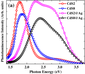
The band at higher energy comes in the energy
range 2.6 eV to 3.4 eV (blue luminescence), whereas
the band at lower energy comes in the energy
range 1.4 eV to 2.4 eV (red luminescence).
The PL peak at higher energy is due to the band
to band transitions, while the peak in lower
energy range is due to defect state transitions.
For uncoated CdS QDs, the PL peak intensity due to
the defect state transitions is much stronger than
the one due to band-to-band transitions.
The defect states arise due to presence of impurities,
cadmium vacancies, sulfur vacancies or from
the surface-dangling bonds.
In case of very small particles, the surface to
volume ratio is very high.
With decreasing particle size, this ratio gets
enhanced and many surface electronic states get
introduced to the system.
As a result, with decreasing particle size,
defect state transitions dominate over band-to-band transitions.
For uncoated CdS samples, the PL peak intensity of
red luminescence is about ten times higher than that
of the blue luminescence. Whereas, in case of
silver-coated CdS nanoparticle solutions, the strength
of the blue and red luminescence are of the same order.
For silver-coated CdS nanoparticles, the thin layer of
silver on top of the semiconductor core, effectively
passivates the surface defect states.
As a result, the PL peak intensity, due to
the defect state transitions, goes down with respect
to the band-to-band transitions.
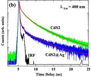
Towards understanding the reason for change of photoluminescence profile in
presence of silver coating, TCSPC experiments have been performed on these uncoated
and silver-coated CdS QD samples.
A picosecond laser of wavelength 375 nm is used
as excitation source and the emission is monitored at 400 nm, which is the PL peak position corresponding to the
band-to-band transitions.
Full width at half maximum (FWHM) of the instrument response function (IRF)
is 250 ps.
The measured TCSPC decay profiles for colloidal solutions of CdS2
and CdS2@Ag QD samples are shown in Fig. 3 (b).
The decay profiles for both the samples could be fitted with three exponential decay function.
The decay lifetime corresponding to the CdS2 QD sample are ps (44.73),
ns (26.70) and ns (28.57).
Whereas, these values for CdS2@Ag sample come out to be ps (75.02),
ps (8.38) and ns (16.60).
The number in the in first bracket gives
the fractional intensity.
It shows that the
faster decay lifetime components corresponding to the
band-edge transitions become even more fast and the
amplitude of fractional intensity become dominant in
case of silver-coated sample compared to uncoated sample.
The presence of metal surface near luminating SQDs may change the spectral profile of the SQDs due to
Förster resonances energy transfer (FRET) from plasmon of
metal to exciton of semiconductor or vice versa
Hosoki et al. (2008); Lakowicz (2005); Chance et al. (2007); Kummerlen et al. (1993).
In the absence of any quenching or enhancing processes, the lifetime () and quantum yield ()
of a SQD are determined by the rate of radiative ()
and nonradiative decay to the ground state ().
The quantum yield and lifetime are given by Schaufele et al. (2005)
, and .
According to the above equation, low quantum yield from SQDs implies .
However, the presence of a metallic surface modifies
the radiative decay rate of an excited SQD. Considering the radiative rate increases to be ,
the quantum yield () and lifetime () of the SQD become
, and ,
respectively.
In principle, can have values from to + .
As the value of increases, the lifetime () decreases and
the quantum yield () increases.
A careful examination of the above equation reveals that high
quantum yields can be obtained whenever is comparable to .
Therefore, it can be concluded that the decrease in decay lifetime in case of silver-coated CdS QDs
is due to resonance energy transfer between plasmon of silver-shell and excitons of CdS-core.
III.3.1 TDPL of uncoated CdS QDs
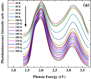
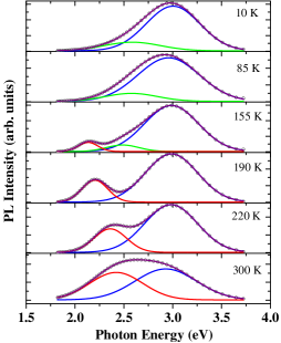
Temperature-dependent photoluminescence (TDPL) has been performed to see the effect of temperature in the photoluminescence properties of these metal / semiconductor composite structures. These experiments are performed on spin coated samples. P-type (111) silicon wafer is used as substrate. The substrates are cleaned using piranha solution, a mixture of sulfuric acid () and hydrogen peroxide (). This technique is used to clean organic residues off substrates. Because the mixture is a strong oxidizing agent, it removes most organic matter, and it also hydroxylates most surfaces (add OH groups), making them highly hydrophilic (water compatible). The room temperature PL spectrum profile gets slightly modified when the experiments are done on the solid thin films. For uncoated solid samples, the peak intensity of the blue luminescence gets slightly enhanced. Whereas, in case of silver-coated samples, it becomes comparatively stronger than the red luminescence. This change in PL spectrum profile is attributed to the interaction between QDs and silicon substrate. Furthermore, with changing temperature, the PL profile changes drastically. Fig. 4 (a) shows the temperature-dependent PL spectra of CdS2 QD sample and the fitting of the PL spectrum at 10 K with six best-fit Gaussians is shown in Fig. 4 (b).
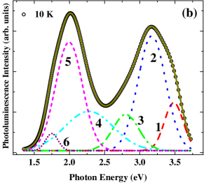
The blue PL band corresponding to band-to-band transitions is fitted with three Gaussians as
the emission spectrum shows two small shoulder peaks
on either side of the main resonance energy peak marked as 2.
The high and low energy PL resonance peaks are attributed to the emission from smaller and larger QDs
present in the sample as shown in Fig. 1 (c).
Whereas, the central PL resonance peak is due to emission from the average size QDs.
The red PL band corresponding to defect state transitions also show two shoulder peaks on either side
of the main defect PL band marked as 5,
and therefore fitted with three Gaussians for all temperatures.
Different nonradiative processes play an important role in relaxation dynamics of SQDs.
The processes, responsible for carrier relaxation in SQDs, are radiative relaxation,
Auger non-radiative scattering Ghanassi et al. (1993), Förster energy transfer between QDs,
thermal escape from the dot, and trapping in surface and/or defect states Yang et al. (1997).
Considering the radiative relaxation, a thermally activated
ionized impurity scattering and the thermal escape of carriers from QDs,
the temperature dependence of the integrated PL intensity can be given by Valerini et al. (2005)
| (2) |
where is the integrated PL intensity at 0 K, (=), and (=) are the constants related to the strength of the involved processes, and is the number of LO-phonons involved in the thermal escape process. To have a deeper insight into these processes, we analyzed the temperature dependence of the integrated PL intensity. The experimental data have been fitted to Eq. 2 by fixing LO-phonon energy meV. Using activation energy meV, the best-fit curve reproduces the experimental data very well (see Fig. 5) for . Furthermore, as the sample temperature increases, the peak position of the central PL band corresponding to band-to-band transitions redshifts as shown in the inset of Fig. 5. This can be attributed to temperature-dependent shift of band-gap which is described by empirically established Varshni relation Varshni (1967):
| (3) |
where is the band-gap energy at 0 K, is the temperature coefficient, and is a constant having value close to Debye temperature of the material. The experimental data has been fitted with Eq. 3. The best-fit curve, with eV/K and K, well reproduces the experimental data, though the Varshni relation is for bulk semiconductor. The value matches well with the theoretically calculated Debye temperature K, which is reported in Yang et al. (2012).
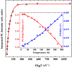
It demonstrates that the peak position shift with temperature is due to the temperature-dependent band-gap shrinkage of CdS, while the confinement energies of the carriers are independent of sample temperature. Apart from the shift of the spectral position of the peak, it has been observed that the FWHM, , of this peak (inset of Fig. 5) increases with sample temperature. Amongst many processes, the exciton-phonon and ionized impurity scattering contribute in modifying FWHM with sample temperature. The line width broadening with increasing sample temperature in case of semiconductor QDs can be explained by the equation Lee et al. (1986),
| (4) |
where is the temperature-independent inhomogeneous broadening which represents fluctuations in size, shape, composition, etc. of the QDs. The second and third terms are related to homogeneous broadening due to exciton-phonon coupling. is the exciton-acoustic phonon coupling coefficient and represents exciton-LO phonon coupling strength. is the LO-phonon energy and is the Boltzmann constant. The fourth term of the Eq. (4) is related to FWHM broadening due to ionized impurity scattering. is the activation energy, required for ionization. The experimental data have been reproduced using the first three terms of Eq. 4. The best-fit is obtained for meV, eV/K, and meV. The LO-phonon energy meV is obtained from the Raman spectrum and kept fixed for the fitting. Thus, it can be concluded that the ionized impurity scattering is not significant for line-width broadening in these CdS QD samples.
In order to understand the origin of the value, we estimated the energy value of the first six excited states from the absorption spectrum of the colloidal solution of CdS QDs. The fitting of the absorption spectrum with six Gaussians is shown in Fig. 6. Inhomogeneous broadening of each excited peak is related to the peak energy and bulk band-gap energy by the following equation Valerini et al. (2005); Norris and Bawendi (1996);
| (5) |
where is relative size dispersion. The energy difference between the first two absorption resonance states is around 218 meV, which is close to the energy of 6.
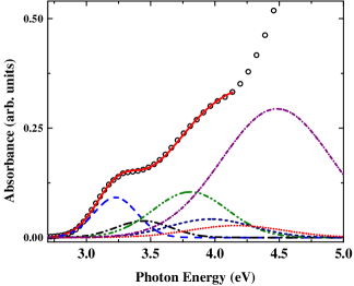
Therefore, it can be concluded that the thermal
escape involves scattering of six LO-phonons.
The experimental defect band spectrum has also been reproduced using
three best-fit Gaussians as shown in Fig. 4 (b).
Fig. 7 shows temperature-dependent
integrated PL intensity of the main defect band (peak position eV) for CdS QDs.
The fitting of temperature-dependent integrated PL intensity is
obtained following equation Jing et al. (2009),
| (6) |
where is the activation energy required to overcome the potential barrier,
A is a parameter that is related to the density of the excited states.
The best-fit curve reproduces the
experimental data points very well for the same activation energy as obtained before.
The inset of Fig. 7 (a) shows the temperature
dependent PL peak position shift and
FWHM broadening of the main defect band (peak position eV) for CdS QDs.
The fitting of temperature dependence of PL peak position is obtained following equation Hsu et al. (2007),
| (7) |
where is LO-phonon energy corresponding to exciton-LO phonon coupling in CdS QD sample. We get best-fit curve for meV. The temperature-dependent FWHM of the main defect band for CdS QDs is shown the inset of Fig. 7 (a). The fitting of temperature-dependent FWHM broadening is obtained following Eq. 4. The best-fit curve reproduces the experimental data points very well for , eV, and meV.
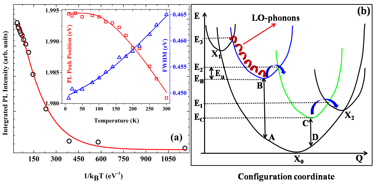
The different temperature-dependent integrated PL intensity behaviour corresponding to band-to-band and defect state transitions for CdS2 QD sample is explained using the configuration coordinate geometry which describes the competitive radiative and nonradiative transitions associated with crossing of the ground and electronic states. Various thermally activated processes are shown in Fig. 7 (b). The integrated PL intensity of the band-to-band PL peak decrease with increasing temperature (see Fig. 5) due to scattering of electrons from the luminating state to some higher energetic dark state by thermal escape through exciton-LO phonon coupling and thermally activated ionization. Whereas, the integrated PL intensity of the main defect PL band increases with temperature (see Fig. 7 a). With increasing sample temperature two competitive processes of carrier generation happen. One is thermally activated electrons jump to the main defect state from higher energetic excited state, and in the other process, electrons get scattered from the main defect band (peak position eV) to higher energetic position through exciton-LO phonon coupling. In this case, with increasing temperature the PL strength of the defect band increase suggesting that the first process dominates over the second process.
III.3.2 TDPL of silver-coated CdS QDs
For the sample CdS2@Ag, the temperature-dependent PL spectra have been shown in Fig. 8.
At room temperature (300 K), the blue luminescence band overlaps with the red luminescence band. However, as we decrease the temperature, these two PL bands become well separated in the temperature range 210 K to 155 K. In addition to that, the red PL peak shifts further towards the red region of the spectrum and the strength of this PL peak goes down and does not appear below 140 K. In the PL spectrum of this sample, one additional structure appears at 155 K temperature. The oscillator strength of this additional structure increases as the temperature is decreased further. This behavior of TDPL spectra of silver-coated CdS QD sample is explained using the configuration coordinate geometry for two different temperature regimes. Fig. 9 depicts the variation of luminescence efficiency due to the change of the relative position of crossover point with temperature.
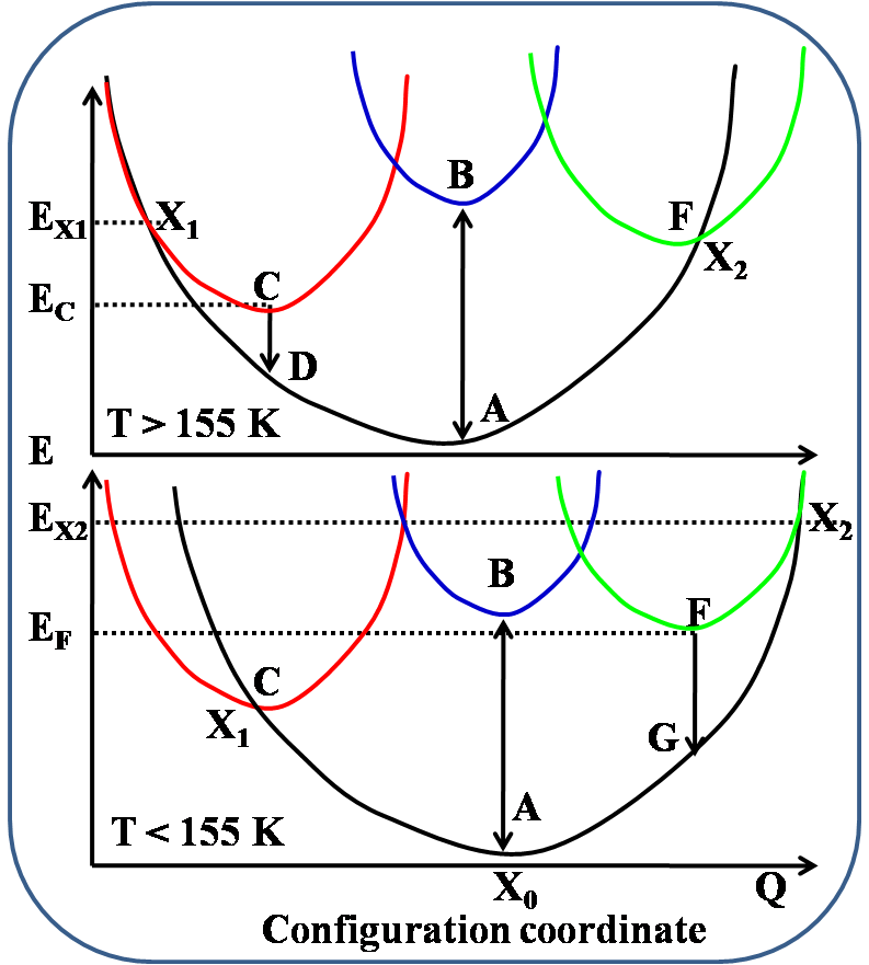
The blue curve is corresponding to the band-edge electronic states, whereas the red and green curves
represent the defect states. After optical excitation, the and transitions give
band-to-band (blue) and defect (red) PL band when the sample temperature is greater than 155 K.
At this temperature regime, there is no radiative transition possible from the point to ground
state as approaches the crossover point . However, as the temperature is lowered, the
ground state moves towards right with respect to the electronic states. Therefore, the red PL band
shifts further towards red region of the spectrum and eventually vanishes when the temperature is
below 155 K as the point approaches and the electrons cool down non-radiatively.
Furthermore, at this temperature regime ( K), the green PL band starts appearing
as the crossover point moves away from the point and initiates radiative transitions ().
Fig. 10 shows temperature-dependent
integrated PL intensity of the main resonance PL band (blue) for CdS2@Ag QDs.
The fitting of temperature-dependent integrated PL intensity is obtained following
Eq. 6.
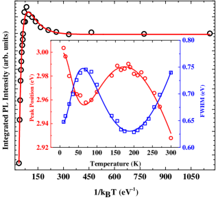
The best-fit curve reproduces the experimental data points very well for , meV, and meV. The PL peak energy of the blue band goes through a successive red-blue-red shift (S-shaped) with increasing sample temperature as shown in the inset of Fig. 10. This anomalous temperature-dependent PL characteristic can be fitted using a thermal carrier redistribution model Lourenco et al. (2007). The fitting of temperature dependence of PL peak position of the blue PL band is obtained following equation,
| (8) |
where is LO-phonon energy corresponding to exciton-LO phonon coupling and is activation energy required for ionization. We get best-fit curve for the same value of as obtained from the temperature-dependent integrated intensity data fitting. Whereas, and values come out to be meV and meV. Inset of Fig. 10 also shows the temperature-dependent FWHM of the main PL band corresponding to band-to-band transitions for CdS2@Ag QDs. It shows a successive blue-red-blue shift (inverted S-shaped) with increasing sample temperature. The fitting of temperature-dependent FWHM broadening is obtained following equation,
| (9) |
The best-fit curve reproduces the experimental data points very well for the same value of and as obtained from the temperature-dependent peak-position data fitting.
IV Conclusions
CdS QDs have been synthesized using -irradiation technique and subsequently silver coating of two QD samples have been prepared. The HRTEM studies confirmed the presence of planes corresponding to hexagonal-wurtzite and cubic zinc-blende crystal structures in the CdS QDs. The absorption spectra of the uncoated CdS QDs show the expected blue-shift of band-edge with respect to bulk CdS, and the absorption spectra of silver-coated CdS QDs show a peak at around 3.4 eV corresponding to the coupling of localized surface plasmon with CdS-core. The PL spectra for coated and uncoated CdS QD samples show two bands corresponding to band-to-band and defect state transitions. In case of uncoated samples, the PL peak intensity corresponding to band-to-band transitions is weaker compared to defect state transitions. However, for silver-coated samples, the band-to-band PL peak intensity gets enhanced by ten times due to coupling of surface plasmon of silver-shell with excitons of CdS-core. Finally, we analyzed the radiative and nonradiative processes involved in the relaxation of uncoated and silver-coated CdS QDs. For CdS QDs, we demonstrated that TDPL is controlled by thermally activated carrier localization with an activation energy of about 20 meV and thermal escape by scattering with six LO-phonons. Whereas, TDPL of silver-coated CdS QDs involves two thermally activated carrier localization states with activation energies of about 24 meV and 4 meV. It also involves thermal escape by scattering with two LO-phonons. These results illustrate the properties of the relaxation processes involved in light emission from uncoated and silver-coated CdS QDs, and are important for future applications in photonics and optoelectronic devices.
References
References
- Sun et al. (2012) L. Sun, J. J. Choi, D. Stachnik, A. C. Bartnik, B.-R. Hyun, G. G. Malliaras, T. Hanrath, and F. W. Wise, Nat. Nano. 7, 369 (2012).
- Son et al. (2012) D. I. Son, B. W. Kwon, D. H. Park, W.-S. Seo, Y. Yi, B. Angadi, C.-L. Lee, and W. K. Choi, Nat. Nano. 7, 465 (2012).
- Huynh et al. (2002) W. U. Huynh, J. J. Dittmer, and A. P. Alivisatos, Science 295, 2425 (2002).
- Klimov et al. (2000) V. I. Klimov, A. A. Mikhailovsky, S. Xu, A. Malko, J. A. Hollingsworth, C. A. Leatherdale, H.-J. Eisler, and M. G. Bawendi, Science 290, 314 (2000).
- Duan et al. (2003) X. Duan, Y. Huang, R. Agarwal, and C. M. Lieber, Nature 421, 241 (2003).
- Harrison et al. (2009) M. T. Harrison, S. V. Kershaw, M. G. Burt, A. L. Rogach, A. Kornowski, A. Eychmüller, and H. Weller, Pure Appl. Chem. 72, 295 (2009).
- Bruchez et al. (1998) M. Bruchez, M. Moronne, P. Gin, S. Weiss, and A. P. Alivisatos, Science 281, 2013 (1998).
- Pompa et al. (2006) P. P. Pompa, L. Martiradonna, A. D. Torre, F. D. Sala, and L. Manna, Nat. Nano. 1, 126 (2006).
- Kalyaniwalla et al. (1990) N. Kalyaniwalla, J. W. Haus, R. Inguva, and M. H. Birnboim, Phys. Rev. A 42, 5613 (1990).
- Mostafavi et al. (2000) M. Mostafavi, Y. Liu, P. Pernot, and J. Belloni, Radiat. Phys. Chem. 59, 49 (2000).
- Valerini et al. (2005) D. Valerini, A. Cretí, M. Lomascolo, L. Manna, R. Cingolani, and M. Anni, Phys. Rev. B 71, 235409 (2005).
- Hsu et al. (2007) W. T. Hsu, K. F. Lin, and W. F. Hsieh, Appl. Phys. Lett. 91, 181913 (2007).
- Frederic et al. (2004) R. Frederic, K. J. Arvind, T. Mona, C. Thierry, Y. Sylvie, L. C. Philippe, Y. L. Chang, P. Seung, Han, and G. C. Joong, Chem. Phys. Lett. 394, 324 (2004).
- Banerjee et al. (2000) R. Banerjee, R. Jayakrishnan, R. Banerjee, and P. Ayyub, Journal of Physics: Condensed Matter 12, 10647 (2000).
- Ricolleau et al. (1998) C. Ricolleau, L. Audinet, M. Gandais, and T. Gacoin, Thin Solid Films 336, 213 (1998), ISSN 0040-6090.
- Gaponenko (1998) S. V. Gaponenko, Optical Properties of Semiconductor Nanocrystals (Cambridge University Press, 1998).
- Nair et al. (1992) S. V. Nair, L. M. Ramaniah, and K. C. Rustagi, Phys. Rev. B 45, 5969 (1992).
- Ghosh et al. (2015) P. Ghosh, K. C. Rustagi, P. Vasa, and B. P. Singh, AIP Conference Proceedings 1661, 100004 (2015).
- Hosoki et al. (2008) K. Hosoki, T. Tayagaki, S. Yamamoto, K. Matsuda, and Y. Kanemitsu, Phys. Rev. Lett. 100, 207404 (2008).
- Lakowicz (2005) J. R. Lakowicz, Anal. Biochem. 337, 171 (2005), ISSN 0003-2697.
- Chance et al. (2007) R. R. Chance, A. Prock, and R. Silbey, Molecular Fluorescence and Energy Transfer Near Interfaces (John Wiley & Sons, Inc., 2007), ISBN 9780470142561.
- Kummerlen et al. (1993) J. Kummerlen, A. Leitner, H. Brunner, F. Aussenegg, and A. Wokaun, Mol. Phys. 80, 1031 (1993).
- Schaufele et al. (2005) F. Schaufele, I. Demarco, and R. N. Day, in Molecular Imaging, edited by A. Periasamy and R. N. Day (American Physiological Society, San Diego, 2005), pp. 72 – 94, ISBN 978-0-19-517720-6.
- Ghanassi et al. (1993) M. Ghanassi, M. C. Schanne‐Klein, F. Hache, A. I. Ekimov, D. Ricard, and C. Flytzanis, Appl. Phys. Lett. 62, 78 (1993).
- Yang et al. (1997) W. Yang, R. R. Lowe-Webb, H. Lee, and P. C. Sercel, Phys. Rev. B 56, 13314 (1997).
- Varshni (1967) Y. Varshni, Physica 34, 149 (1967), ISSN 0031-8914.
- Yang et al. (2012) X. X. Yang, Z. F. Zhou, Y. Wang, R. Jiang, W. T. Zheng, and C. Q. Sun, J. Appl. Phys. 112, 083508 (2012).
- Lee et al. (1986) J. Lee, E. S. Koteles, and M. O. Vassell, Phys. Rev. B 33, 5512 (1986).
- Norris and Bawendi (1996) D. J. Norris and M. G. Bawendi, Phys. Rev. B 53, 16338 (1996).
- Jing et al. (2009) P. Jing, J. Zheng, M. Ikezawa, X. Liu, S. Lv, X. Kong, J. Zhao, and Y. Masumoto, J. Phys. Chem. C 113, 13545 (2009).
- Lourenco et al. (2007) S. A. Lourenco, I. F. L. Dias, J. L. Duarte, E. Laureto, V. M. Aquino, and J. C. Harmand, Braz. J. Phys. 37, 1212 (2007), ISSN 0103-9733.