Dynamical properties of bidirectional charge-density-waves in ErTe3
Abstract
We report a strong difference in the sliding properties of the bidirectional charge density wave (CDW) in the two-dimensional rare earth tritelluride ErTe3 which occurs below K with a wave vector along -axis and below K with a wave vector along -axis; the excess current carried by the motion of the CDW is 10 times less for the lower CDW compared with the value of the upper one. We tentatively explain this result by a stronger pinning of the lower temperature CDW intricated with the upper one, which inhibits its motion and may generate a phase slippage lattice.
pacs:
72.15.Nj, 71.45.Lr, 61.44.FwI Introduction
Symmetry-breaking phase transitions with interplay between multiple degrees of freedom are intensively studied in strongly correlated systems such as high- superconductors, modulated charge or spin structures (charge/spin density waves) and another ordered states. A charge density wave (CDW) is characterized by a spatial periodic modulation of the electronic density concomitant with a lattice distortion with the same periodicity inducing the opening of a gap, , in the electronic dispersion. The collective properties of the CDW quantum state can be described by a complex order parameter with the collective excitations of and being the amplitude and phase modes.
Although theoretically predicted by Kohn Kohn59 , Overhauser Overhauser62 , Peierls Peierls55 and Fröhlich Frohlich54 in the 1950s and 1960s, the first Peierls-Fröhlich transition was experimentally observed nearly simultaneously in the beginning of 1970s in quasi-one dimensional systems – linear Pt-chain material Comes [K2Pt(CN)4Br0.30xH2O], organic tetrathiafulvalene- tetracyanoquinodimethane salt (TTF- TCNQ)(see for review Heeger ), and quasi-two dimensional transition metal dichalcogenides MX2 (M: Nb, Ta; X: S, Se)MX2 . Then a few years later, CDW transitions were found in transition metal trichalcogenides, NbSe3, TaS3Monceau12 and in molybdenium bronze K0.3MoO3bronze .
In one hand, from 1D weak coupling mean field theories, with , the Peierls instability is driven by the electronic energy gain which originates mostly from the Fermi surface nesting with . In the other hand, in the strong limit coupling, , as recognized by McMillanMcMillan77 and Varma and SimonsSimons83 the transition is driven by the entropy of the lattice; the energy gain is then spread over the entire Brillouin zone as recently observed by inelastic neutron scatteringNScatt . As the electron phonon coupling is increased the importance of the electronic structure in -space is reduced and a local chemical bonding picture in real space is more appropriate.
One of the most representative features of one-dimensional (1D) compounds with a charge-density wave (CDW) is the possibility of collective electron transport first predicted by H. Fröhlich Frohlich54 , as a model for superconductivity in 1D. The extraconductivity which results from the CDW sliding is a collective motion of electrons, a mechanism totally different from the classical one of elastic scattering of individual electrons which leads to the residual resistance. However various mechanisms such as impurities, defects, interchain interaction or commensurability pin the phase of the CDW and at low electric field the conductivity exhibits a constant ohmic behavior due to quasi-particle excitations only. To overcome the pinning energy and to initiate the CDW sliding it is necessary to apply an electric field of a sufficient strength larger than some characteristic threshold electric field, Gruner ; Monceau12 . At the present time sliding CDW properties have been observed and well studied in many inorganic as well as in organic one-dimensional compounds (for recent review, see Ref. Monceau12, ).
Since many years, the search of a possible CDW sliding in two dimensional (2D)compounds was unavailing. Only recently it was succeeded in observing collective CDW motion in quasi-2D rare-earth tritellurides compounds SinchPRB12 ; SSC14 . This new family of quasi-2D compounds has raised an intense research activity last time DiMasi95 ; Brouet08 ; Ru08 , because it is considered as a model system for which the structure of the CDW ground state can be theoretically studied Yao06 . Thus a phase diagram as a function of the electron-phonon parameter was derived with a bidirectional (checkerboard) state if the CDW transition temperature is sufficiently low whereas a unidirectional stripe state, as observed experimentally, occurs when the transition temperature is higher. This result is relevant for a deeper understanding of the charge pattern in highly correlated materials, and particularly to the recent determination of the biaxial CDW in underdoped cuprates LeBoeuf2013 .
Te3 (=Y, La, Ce, Nd, Sm, Gd, Tb, Ho, Dy, Er, Tm) layered compounds have a weakly orthorhombic crystal structure (space group ). They are formed of double layers of nominally square-planar Te sheets, separated by corrugated Te slabs. In this space group, the long axis is perpendicular to the Te planes. These systems exhibit an incommensurate CDW below the Peierls transition temperature through the whole series Ru08 ; Lavagnini10R , with a wave vector , with above 300K for the light atoms (La, Ce, Nd). For the heavier (Tb, Dy, Ho, Er, Tm) atoms a second CDW occurs at low temperature with the wave vector perpendicular to . The superlattice peaks measured from X-ray diffraction are very sharp and indicate a long range 3D CDW order Ru08 .
Below the Peierls transition, in all Te3 compounds, the Fermi surface is partially gapped resulting in a metallic behavior at low temperature. The layered Te3 compounds exhibit a large anisotropy between the resistivity along the -axis and that in the plane, typically below and much higher at low temperature Ru06 . Because the unidirectional character of the upper CDW Fang07 ; Lavagnini10R ; Yao06 , a conductivity anisotropy in the plane arises in the CDW state as was observed experimentally and explained theoretically in Ref. sinchPRL14, . The effect of the upper CDW on the in-plane resistivity observed in experiments is very weak, no more than a few percents of the total resistance Ru08 ; sinchPRL14 ; Ru06 .
Amplitude CDW excitations were probed by Raman spectroscopyLavagnini10R , time-resolved ARPESLeuenberger15 and femtosecond pump-probe spectroscopyYusupov08 ; Moore16 . This later technique has allowed to study the disentanglement of the electronic and lattice path of the CDW order parameter, the collective vibrations being assigned to amplitude modes. On the other hand, collective charge phase excitations could not be observed in far-infrared measurements due to screening by the residual metallic component of the Fermi surface. But the phase collective mode is accessible through non-linear transport properties.
Thus, effect of collective electron transport was observed for the high temperature CDW in single crystals of DyTe3SinchPRB12 , TbTe3 and GdTe3SSC14 but only when the electric field is applied along the -direction, namely -axis. Sliding effect is completely absent when the current is applied in the perpendicular, -axis direction, demonstrating the unidirectional character of the high-T CDW. No attempt up to now was made at observing the possible sliding of the low-T CDW in RTe3.
Among all CDW compounds, only a few exhibit multiple CDWs. In MX2 compounds, a triple structure is formed with three wave vectors of equal amplitude, 120o apartMX2 . In TTF- TCNQ a Peierls transition occurs first on TCNQ stacks at 54 K, a second CDW transition on parallel TTF stacks at 49 K which drives the transverse modulation along from to a locked value at 38 KComes . Both CDWs in NbSe3 are formed on two different parallel chainsMonceau12 .
Hereafter we report measurements of CDW sliding properties of ErTe3 which exhibit two CDWs at K and K. The situation is unique. Unlike NbSe3 where both CDWs slide along parallel different chains, both CDWs in ErTe3 exist within the same Te-planes, thus both CDWs modulate the positions of the same Te atoms. The main questions we would like to answer are the following:
(i) is it possible to detect the sliding of the low-T CDW, besides the fact that the anomaly of resistivity at is barely visible?
(ii) is there any change of the sliding of the high-T CDW below ?
(iii) are these orthogonal CDWs totally independent or are they interacting one with the other? If yes, what is the result and the mechanism of this interaction?
II Experimental
Single crystals of ErTe3 were grown by a self-flux technique under purified argon atmosphere as described previously SinchPRB12 . For experiments we chose good quality single crystals. Thin single-crystal samples with a thickness less than 2 m were prepared by micromechanical exfoliation of relatively thick crystals glued on a sapphire substrate. The quality of selected crystals and the spatial arrangement of crystallographic axis were controlled using X-ray diffraction techniques. X-ray diffraction measurements show that single crystals with a thickness more than 2 m as a rule are twinned with the change between and axis in neighboring layers. However, for thinner samples it was possible to select untwinned single crystals with well defined crystallographic axis positions.
From untwinned single crystals with a thickness typically 0.2-2.0 m, we cut stripes with a length of a few mm and a width m in well defined orientation, namely [100] and [001]. In the following we call -axis stripes samples with the length along the [001] direction and -axis stripes those with the length along [100]. In some cases it was succeeded to select native crystals with a shape of a narrow stripe with a width 50-100 m and length near 1 mm, oriented along -axis. Measurements of current-voltage characteristics (IVs) and their derivatives have been performed with a conventional 4-probe configuration. For contacts preparation we used gold evaporation and cold soldering by In. The current was applied along the length of the stripes. For studying nonstationary effects a radiofrequency (rf) current was superposed on the dc current using current contacts connected with the generator via two capacitors. All measurements have been performed in the temperature range 4.2-340 K.
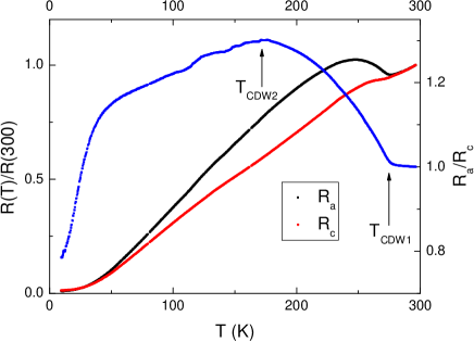
Example of temperature dependencies of the normalized resistance, , for - and -axis stripes and conductivity anisotropy, is shown in Fig.1. The difference between the T-dependence of and is a clear indication that the sample is untwinned. The dependencies shown in Fig.1 corresponds qualitatively to those reported in Ref. sinchPRL14, for DyTe3, HoTe3 and TbTe3. However, one can note the decrease of anisotropy below 40 K the origin of which needs further investigations.
III Experimental results
III.1 high-T CDW
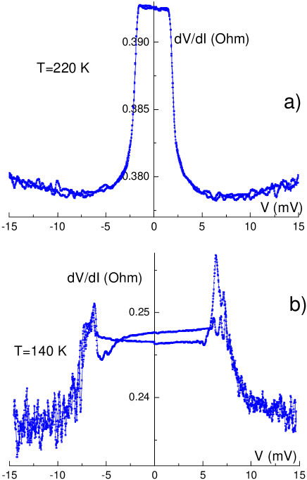
As reported before, the collective CDW motion for the high-T CDW is observed only in -axis stripes. We were able to measure characteristic nonlinearity in IV curves below down to 100 K; the conductivity of the stripe increases sharply above a threshold electric field. However, the shape of IV characteristics change qualitatively for temperatures slightly above and below as demonstrated in Fig. 2. As can be seen, at temperatures below IV curves become hysteretic and much more noisy. Additionally, sharp maxima of appear at electric field close to .
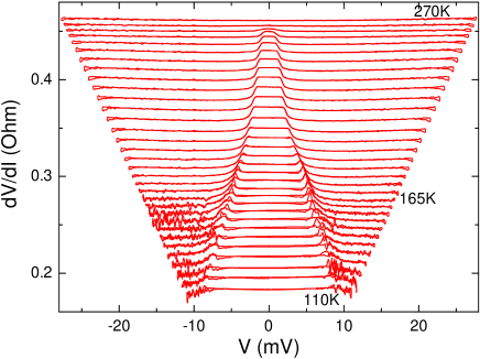
The temperature evolution of differential IV curves in the temperature range 270-110 K for one of the stripes is shown in Figure 3. Neighbour curves differ by K. The same behavior was observed for another stripes. Note that the relative change of the differential resistance from static to sliding state is very small, no more than 3% from the total resistance, indicating a very low contribution of the CDW to the electron transport.
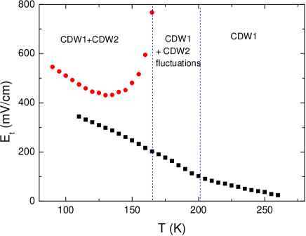
It can be seen as drawn in Fig.8 that the threshold electric field increases monotonically with the decrease of temperature but in the temperature range K increases more rapidly. Nearly the same effect was observed in the quasi-one dimensional NbSe3 for high-T CDW at temperatures close to the second CDW transition Q1Q2 . Note that in these -axis stripes (with the current applied along the -axis) below there are no indication of sliding of the low-T CDW the -vector of which being along -axis.
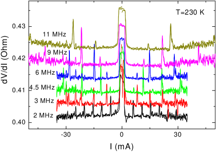
CDW sliding is accompanied by low-frequency broadband electric noise (BBN) and narrowband noise (NBN). The collective electronic transport and the NBN generation can be characterized in terms of the CDW coherence and homogeneity of the CDW in space and in time. The coherence can be affected by external rf (or hf) irradiation. The most widely studied effect of the irradiation is the synchronization of the CDW, known also as the interference effect, mode locking, or Shapiro steps.Monceau12 . In the present study we have observed Shapiro steps at such experimental conditions. Fig.4 shows dependencies at K under application of a rf field with different frequencies from 2 MHz up to 11 MHz with the rf ac field amplitude of 900 mV. Shapiro steps are clearly observed in the characteristics at all frequencies as sharp maxima in the differential resistance demonstrating high level coherency of the CDW.
It is interesting also to trace the evolution of Shapiro steps with temperature at fixed frequency. Fig. 5 shows curves under application of a rf field with MHz and amplitude V at different temperatures. As can be seen, Shapiro steps are clearly observed only down to temperatures close to . Close to this temperature the amplitude of Shapiro steps starts to decrease that indicates the loss of coherency of the high-T CDW in the temperature range where the low CDW occurs.
As shown in Fig.4 the separation between Shapiro steps increases when the rf-frequency increases. Having two contributions to the electric current: normal electrons and collective CDW transport, can be easy calculated using dc IV characteristics:
| (1) |
where - total current, - actual resistance of the sample and - normal state resistance.
III.2 low-T CDW
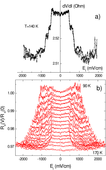
In -axis stripes prepared from untwinned single-crystals we succeeded to observe collective motion for the low-T CDW. A typical IV curve demonstrating characteristic CDW non-linearity at K well below is shown in Fig. 6(a). As can be seen, at V/cm, the differential resistance sharply decreases.
The temperature evolution of differential IV curves in the temperature range 90-170 K for the same sample is shown in Figure 6(b). The curves are shifted for clarity and the difference between each of them is K. As can be seen, the threshold electric field weakly decreases with the increase of in the range 90-150 K. In contrast to the high-T CDW, at temperatures close to K starts to increase indicating divergency at . Such a behavior has been previously observed in quasi-1D compounds with a CDW Monceau12 . The T-dependence of the threshold field for the low-T CDW is plotted in Fig.8. There are no any non-linearity in the IV-characteristics at temperatures above K except a very weak Joule heating. Note that the observed contribution to the electron transport from the low-T CDW sliding is nearly 4 times less compared with the high-T CDW and its amplitude is no more than 0.7% from the total current.
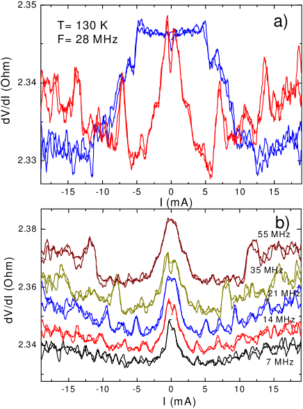
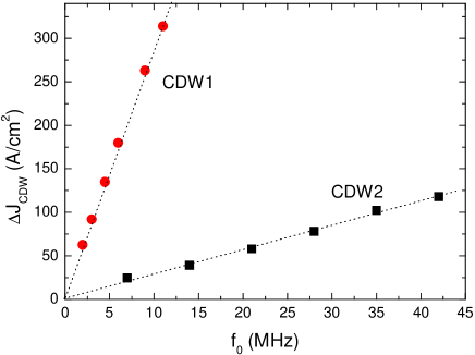
To confirm that the observed non-linearity of IV curves is the real sliding of the low-T CDW we measured IV characteristics under application of dc and rf electric field. As in the case of the high-T CDW, in spite of the low amplitude in the sliding effect, we observed pronounced Shapiro steps however. Figure 7(a) shows dependencies at K under application of a rf field with a frequency of 28 MHz and amplitude 0.9 V. For comparison, the static (without rf field) differential IV curve (blue) measured at this temperature is also shown. Note that the application of a rf electric field leads to a reduction of the threshold electric field . At the same time, Shapiro steps appear in the characteristics as sharp maxima in the differential resistance. With increasing frequency the distance between neighboring maxima increases proportionally to the frequency; that is illustrated in Fig. 7(b) where we show IV curves under application of a rf field with a frequency of 7, 14, 21, 35 and 55 MHz at the same temperature and with the same rf power. The curves are shifted relative to each over for clarity. The excess current density calculated from Eq.1 (with the cross-section of the sample cm-2) is plotted in Fig.9 as a function of rf frequency. As for the upper CDW linearly increases with frequency.
IV Discussion
The RTe3 family (R: La, Ce, Pr, Nd, Gd, Tb, Dy, Er, Tm) is a model system for studying the effect of chemical pressure on the Peierls transition due to a reduction of the in-plane lattice constant from light R (La, Ce, …) towards heavier R ions (Dy, Er, Tm). While the wave vector along -axis (which results from charge transfer between RTe buckled planes and Te planes) is nearly the same for each member of the family, the Peierls transition temperature is much larger than room temperature for light R and decreases below room temperature for heavier R Ru08 . From optical spectroscopy Sachetti09 and ARPES measurements Brouet08 it was shown that the CDW gap scales with the lattice parameters. In addition, optical measurements Pfuner10 have revealed that the remaining fraction of ungapped FS in the CDW state is larger for compounds with smaller lattice parameters. Thus phenomenologically, it was suggested that a second CDW is formed only when the first CDW is weakened with the decrease of the lattice parameter, making larger FS sections available for the new nesting condition in the transverse -axis.
While ARPES measurements Brouet08 are interpreted as a strong evidence for a FS nesting scenario, inelastic x-ray scattering Maschek15 and Raman experiments Eiter13 emphasize the strongly momentum-dependent electron-phonon coupling. In that case, a local chemical description of the distortions is more realistic, as proposed in Ref.Malliakas06, where the distortion of the Te net is viewed as an oligomer sequence of Te trimers and tetramers.
As far as ErTe3 is concerned, only a few publications are available. The low-T CDW was discovered by Ru et al.Ru08 .The superstructures and (measured at K) are sharp. Both wave vectors are present in the same crystallite. The integrated intensity of exhibit large fluctuations above , at least up to 180 K. The CDW gaps were determined by ARPES Moore10 with meV and meV with the temperature dependence of slightly suppressed from the mean-field variation. These values are in agreement with those measured by Raman scattering Eiter13 . The ratio is much larger than the BCS mean field 3.52 value, similarly to many one-dimensional systemsMonceau12 indicating strong coupling effect or the role of fluctuations.The observation of the amplitude mode by Raman scattering Eiter13 such with the frequency of the unnormalized CDW phonon energy yields indicating strong coupling.
It has to be noted Moore10 that the lower CDW is weaker with
| (2) |
The density of states was calculated from the interacting tight-binding model. The onset of the high-T CDW suppresses by 77% of the unmodulated value while the low-T CDW further suppresses by 74% revealing that the gain in the second CDW is really modest Moore10 .
Many models for the RTe3 electronic structure consider only Te planes, sometimes a single one; the buckled Te slabs are viewed as a simple charge reservoir that determines the Fermi level with the f states of the rare earth localized away from the Fermi surface and expected to play no role. However the hybridization between the rare-earth 4f electrons and Te 2p electrons was revealed Lee12 by the observation of a diffraction peak near the M5(3d-4f) absorption edge of rare-earth ions with a wave vector identical to that of the CDW.
We have experimentally measured nonlinear transport properties in ErTe3 associated to each CDW, the upper one with current applied parallel to along -axis, and the lower one with along -axis. Are these nonlinearities the signature of the Fröhlich-type conductivity as demonstrated Monceau12 in quasi one-dimensional compounds?
As was mentioned in section I, it is assumed that both CDWs exist within the Te planes and that both CDWs modulate the position of the same Te atoms. The possibility that CDWs occur on a different Te plane of the Te bilayer is very unlikely, although evoked in Ref.19. However it is worth to note that by Raman scattering experiments, the amplitude mode in the high-T CDW develops as a succession of two mean field transitions with different critical temperatures; that was associated to the Te bilayers Lavagnini10R .
The main results we have obtained can be summarized as follows: in cooling, when approaching the bidirectional CDW ground state at K, the threshold field of the high-T CDW increases more than linearly, noise appears in the differential IV characteristics and the high-T CDW coherence is lost by the disappearance of Shapiro steps. In Fig. 8 we have plotted the temperature dependence of the threshold electric field for both CDWs. Taking into account the fact that the absolute value of is sample dependent and that the threshold characteristics of high- and low-T CDWs were measured in different stripes, exfoliated however from the same single crystal, the curves in Fig. 8 demonstrate only the qualitative behavior of .
As can be seen, in the temperature range 270-200 K the dependence of the upper CDW is linear and can be well described by the expression:
| (3) |
with mV/cm and similarly to the behavior of for the upper CDW reported previously SSC14 . In the range 200-165 K we observe a deviation from the linear dependence and increases more rapidly in this temperature range. At temperature K, resumes again a linear dependence. We understand such a behavior as the result of interaction between high-T and low-T CDWs. Indeed it has been shown that fluctuations of the low-T CDW extend up to nearly 200 K Ru08 .
The depinning process for the unidirectional CDW, namely in TbTe3 at room temperature, has been probed by coherent x-ray diffraction Bolloch16 .Contrary to one-dimensional systems (such as NbSe3 and K0.3MoO3)Monceau12 the CDW remains undeformed below threshold and suddenly rotates to overcome pinning centers and reorders by motion above threshold.
In a superfluid there are a macroscopic occupation of a quantum state that picks out a unique reference frame which describes the velocity of the superfluid. In a superconductor it is the common momentum of Cooper pairs that defines . In the Fröhlich model, as stated by Allender et al.Allender74 , is determined by the velocity of the macroscopically occupied lattice wave which produces energy gaps. Then the extracurrent carried by the CDW into motion is . The frequency of Shapiro steps in differential IV characteristic was identified as the signature of the CDW velocity with with : the CDW wavelength. In Fig. 9 we have plotted together the excess current density in the nonlinear state of ErTe3 as a function of the frequency of Shapiro steps for the high-T CDW at K and the low-T CDW at K. For the high-T CDW, in Fig. 9 we can evaluate the ratio JCDW1 / f0 = 28 A/MHz cm2. This value is very similar to the average value obtained on 14 samples for the upper CDW on NbSe3: 40.2 A/MHz cm2 and 24 A/MHz cm2 for the lower one Richard93 . Similar values were also obtained for o-TaS3 Zettle83 ; Sokoloff90 .
In a one-band model (or for one chain in 1D description), and the condensate density is . Then
| (4) |
This relation is well satisfied in 1D systemsMonceau12 and demonstrates the Fröhlich-type of conductivity.
Determining a similar value of for the high-T CDW in ErTe3 indicates that the same Fröhlich process is operating. Let consider the number of unit cells in the cross section of our sample with the lattice parameters and , one get unit cells. Consider also that along the -axis, one have one Te chain per unit cell. Then we recover the value of A/MHz cm2.
We can also estimate the CDW velocity. At K, at the total current applied mA, we have evaluated mA. With the electron density cm-3 and taking into account that no more than 30%-40% of the FS is affected by the formation of the CDW Lavagnini10R , we get a very small value of the CDW velocity cm/s. However the number of carriers condensed below the CDW gap needs to be verified.
While the sliding properties of the high-T CDW appear to correspond to the Fröhlich mechanism, the situation is totally different for the low-T CDW. From Fig. 9 we deduce the slope of 10 times lower than the value for the high-T CDW. Additionally the threshold field is higher. This result is opposite to NbSe3 with both CDWs sliding along parallel chains and for which the is nearly the same for both CDWs Richard93 .
We can only speculate on a possible explanation of these results. The bidirectional CDW is formed by two orthogonal modulations of Te atoms which naturally interact and are imbricated. Because the sliding is along -axis for the high-T CDW and along -axis for the low-T CDW, the coupling between them, say bonds, should be broken. The crystallographic structure should have an important role. It was shown Ru08 that the formation of the high-T CDW (in TbTe3) appears to ”stretch” the lattice from its expected value along the direction of the modulation wave vector (-axis). It is also the direction of the glide between the two Te planes. Then the depinning along -axis may appear to be easier, even if the high-T CDW looses its coherence when crossing .
From the general Fröhlich mechanism, with the current carried by the motion of the CDW as and with identified from Shapiro steps as , then . In ErTe3 the slop is 10 times less for the lower CDW with respect to the upper one. One may then suggest that the full electronic density condensed below the gap in the band of low CDW, as in the Fröhlich model, does not participate to the conductivity but only a part of it, namely arround . Pinning along -axis may be stronger and the bond between both modulations anisotropic. Nonlinearity may result from the motion of a lattice of phase defects which is formed in the checkerboard lattice of both CDWs.
This interpretation needs naturally to face some experimental results. It appears to determine the modulated structure of ErTe3 in the unidirectional CDW state as well as in the bidirectional one. STM measurements at low temperature are also crucial as well as a theoretical model for sliding of a bidirectional CDW. However, STM images may be difficult to be interpreted because possibly blurred by the disorder Robertson06 of the bidirectional superstructure.
In conclusion we have observed the nonlinearity in transport properties of the bidirectional charge density wave ground state of ErTe3. While the sliding properties of the upper CDW appear to be similar to those previously found in quasi one-dimensional systems, the nonlinearity for the lower CDW may involve a phase defect lattice. More works are naturally needed to ascertain or weaken the present interpretation.
Acknowledgements.
The work has been supported by Russian State Fund for the Basic Research (No. 14-02-01126–a), and partially performed in the frame of the CNRS-RAS Associated International Laboratory between CRTBT and IRE ”Physical properties of coherent electronic states in coherent matter”.References
- (1) W. Kohn, Phys. Rev. Lett. 2, 393 (1959).
- (2) A.W. Overhauser, Phys. Rev. 128, 1437 (1962).
- (3) R.E. Peierls, Quantum Theory of Solids, Oxford University, Oxford, 1955, p. 108.
- (4) H. Fröhlich, Proc. Roy. Sos. A223, 296 (1954).
- (5) R. Comes and G. Shirane, in: J.T. Devresse, R.P. Evrard and V.E. van Doren (Eds.), Highly Conducting One-Dimensional Solids, Plenum Press, NewYork, 1979, p.17
- (6) A. J. Heeger, in: J.T. Devresse, R.P. Evrard and V.E. van Doren (Eds.), Highly Conducting One-Dimensional Solids, Plenum Press, NewYork, 1979, p.69
- (7) J.A. Wilson, F.J. Di Salvo and S. Mahajan, Advances in Physics 24, 117 (1975).
- (8) P. Monceau, Advances in Physics 61, 325 (2012).
- (9) C. Schlenker (Ed.), Low-Dimensional Electronic Properties of Molybdenum Bronzes and Oxides, Kluwer Academic Publishers, Dordrecht, 1989.
- (10) W.L. McMillan, Phys. Rev. B 16, 643 (1977).
- (11) S.M. Varma and A.L. Simons, Phys. Rev. Lett. 51, 138 (1983).
- (12) F. Weber, S. Rosenkranz, J.-P. Castellan, R. Osborn, R. Hott, R. Heid, K.-P. Bohnen, T. Egami, A. H. Said, and D. Reznik, Phys. Rev. Lett. 107, 107403 (2011).
- (13) G. Grüner, Density Waves in Solids (Addison – Wesley, Reading, Massachusetts, 1994), L. Gor’kov and G. Grüner Charge Density Waves in Solids (Amsterdam: Elsevier Science, 1989), Electronic Crystals 08 edited by S. Brazovskii, P. Monceau and N. Kirova, (Physica B, vol 404, Issues 3-4, 2009).
- (14) A.A. Sinchenko, P. Lejay, and P. Monceau, Phys. Rev. B 85, 241104(R) (2012).
- (15) A.A. Sinchenko, P. Lejay, O. Leynaud and P. Monceau, Solid State Communications 188, 67 (2014).
- (16) E. DiMasi, M. C. Aronson, J. F. Mansfield, B. Foran, and S. Lee, Phys. Rev. B 52, 14516 (1995).
- (17) V. Brouet, W. L. Yang, X. J. Zhou, Z. Hussain, R. G. Moore, R. He, D. H. Lu, Z. X. Shen, J. Laverock, S. B. Dugdale, N. Ru, and I. R. Fisher, Phys. Rev. B 77, 235104 (2008).
- (18) N. Ru, C. L. Condron, G. Y. Margulis, K. Y. Shin, J. Laverock, S. B. Dugdale, M. F. Toney, and I. R. Fisher, Phys. Rev. B 77, 035114 (2008).
- (19) H. Yao, J.A. Robertson, Eun-Ah Kim, and S.A. Kivelson, Phys. Rev. B 74, 245126 (2006).
- (20) D. LeBoeuf, S. Krämer, W.N. Hardy, R. Liang, D.A. Bonn and C. Proust, Nature Phys., 9, 79 (2013).
- (21) M. Lavagnini, M. Baldini, A. Sacchetti, D. Di Castro, B. Delley, R. Monnier, J.-H. Chu, N. Ru, I. R. Fisher, P. Postorino, and L. Degiorgi, Phys. Rev. B 81, 081101(R) (2010).
- (22) N. Ru and I. R. Fisher, Phys. Rev. B 73, 033101 (2006).
- (23) A. Fang, N. Ru, I. R. Fisher, and A. Kapitulnik, Phys. Rev. Lett. 99, 046401 (2007).
- (24) A.A. Sinchenko, P.D. Grigoriev, P. Lejay, and P. Monceau, Phys. Rev. Lett. 112, 036601 (2014).
- (25) D. Leuenberger, J. A. Sobota, S.-L. Yang, A. F. Kemper, P. Giraldo-Gallo, R. G. Moore, I. R. Fisher, P. S. Kirchmann, T. P. Devereaux, and Z.-X. Shen, Phys. Rev. B 91, 201106(R) (2015).
- (26) R. V. Yusupov, T. Mertelj, J.-H. Chu, I. R. Fisher, and D. Mihailovic, Phys. Rev. Lett. 101, 246402 (2008).
- (27) R. G. Moore, W. S. Lee, P. S. Kirchman, Y. D. Chuang, A. F. Kemper, M. Trigo, L. Patthey, D. H. Lu, O. Krupin, M. Yi, D. A. Reis, D. Doering, P. Denes, W. F. Schlotter, J. J. Turner, G. Hays, P. Hering, T. Benson, J.-H. Chu, T. P. Devereaux, I. R. Fisher, Z. Hussain, and Z.-X. Shen, Phys. Rev. B 93, 024304 (2016).
- (28) R. G. Moore, V. Brouet, R. He, D. H. Lu, N. Ru, J.-H. Chu, I. R. Fisher, and Z.-X. Shen, Phys. Rev. B, 81, 073102 (2010).
- (29) H.-M. Eiter, M. Lavagnini, R. Hackl, E.A. Nowadnick, A.F. Kemper, T.P. Devereaux, J.-H. Chu, J.G. Analytis, I.R. Fisher, L. Degiorgi, PNAS, 110(1), 64 (2013).
- (30) A.A. Sinchenko and P. Monceau, Phys. Rev. B, 87, 045105 (2013).
- (31) A. Sacchetti, C. L. Condron, S. N. Gvasaliya, F. Pfuner, M. Lavagnini, M. Baldini, M. F. Toney, M. Merlini, M. Hanfland, J. Mesot, J.-H. Chu, I. R. Fisher, P. Postorino, and L. Degiorgi, Phys. Rev. B, 79, 201101R (2009).
- (32) M. Maschek, S. Rosenkranz, R. Heid, A. H. Said, P. Giraldo-Gallo, I. R. Fisher, and F. Weber, Phys. Rev. B, 91, 235146 (2015).
- (33) W. S. Lee, A. P. Sorini, M. Yi, Y. D. Chuang, B. Moritz, W. L. Yang, J.-H. Chu, H. H. Kuo, A. G. Cruz Gonzalez, I. R. Fisher, Z. Hussain, T. P. Devereaux, and Z. X. Shen, Phys. Rev. B, 85, 155142 (2012).
- (34) D. Le Bolloc’h, A.A. Sinchenko, V.L.R. Jacques, L. Ortega, J.E. Lorenzo, G. Chahine, P. Lejay, and P. Monceau, Phys. Rev. B, 93, 165124 (2016).
- (35) David Allender, J. W. Bray, and John Bardeen, Phys. Rev. B, 9, 119 (1974).
- (36) J. Richard, J. Chen, S.N. Artemenko, Solid State Communications, 85, 605 (1993).
- (37) A. Zettl and G. Grüner, Phys. Rev. B, 28, 2091 (1983).
- (38) J. B. Sokoloff, Phys. Rev. B, 42, 760 (1990).
- (39) C. D. Malliakas and M. G. Kanatzidis, J. Am. Chem. Soc., 128 (2006) 12612.
- (40) F. Pfuner, P. Lerch, J.-H. Chu, H.-H. Kuo, I. R. Fisher and L. Degiorgi, Phys. Rev. B, 81, 195110 (2010)
- (41) J. A. Robertson, S. A. Kivelson, E. Fradkin, A. C. Fang and A. Kapiltunik, Phys. Rev. B, 74, 134507 (2006)
