Multigap superconductivity and interaction driven resonances in superconducting nanofilms with an inner potential barrier
Abstract
We study the crossover in a zero temperature superconducting nanofilm from a single to a double superconducting slab induced by a tunable insulating potential barrier in the middle. The single phase superconducting ground state of this heterostructure is shown to be intrinsically multigapped and to have a new type of resonance caused by the strength of the barrier, thus distinct from the Thompson-Blatt shape resonance which is caused by tuning the thickness of the film. Single particle electronic states are strongly or weakly affected according to their parity (even or odd) with respect to the insulating barrier. The lift of the parity degeneracy at finite barrier strength reconfigures the pairing interaction and leads to a multigapped superconducting state with interaction driven resonances.
pacs:
74.20.Fg, 74.78.-w, 74.78.NaI introduction
Since two-gap superconductivity has been discovered in MgB2 Liu et al. (2001); Giubileo et al. (2001, 2002); Iavarone et al. (2002, 2005); Kortus et al. (2001); Bianconi et al. (2007) an intense research activity has been devoted to multiband and multigap superconductors. In fact two-gap superconductivity has been theoretically proposed long ago Suhl et al. (1959); Moskalenko et al. (1991) and recently found in many compounds Perucchi et al. (2012) ranging from composites Abdel-Hafiez et al. (2015) to metallic Pb Floris et al. (2007); Ruby et al. (2015). Nano-engineered superconducting films tailored to atomic precision thickness Guo et al. (2004); Bao et al. (2005); Zhang et al. (2010) are pivotal to this research as they display multibands and multigapped superconductivity. Superconductivity in ultrathin nanofilms was demonstrated to be very robust and it can survive even in monoatomic layers of In and PbZhang et al. (2010).
In this paper we show that the superconducting nanofilm with an inner potential barrier has an intrinsic multigap structure. Interestingly a nanofilm with a single superconducting slab has multibands but only displays multigaps within the narrow window of shape resonances, as shown by Thompson-Blatt Thompson and Blatt (1963). However this narrow window, defined by the nanofilm width and by the pairing energy scale, renders very difficult its experimental observation. To overcome this problem we consider here a SIS nanofilm, a superconductor-insulator-superconductor “sandwich” such that the two superconductors are thin slabs in the quantum-size regime separated by a very thin insulating slab. We show here that the SIS nanofilm is multigapped since it remains so whether or not in a shape resonance. We also show that the SIS nanofilm possesses a new type of resonance hereafter called interaction driven resonance to distinguish from the well-known shape driven resonance occurring in the single slab superconducting nanofilm. The SIS nanofilm displays very distinct and novel properties with respect to the single slab nanofilm. They stem from the additional parity properties with respect to the insulating barrier since single particle states can be either even or odd. Even states strongly feel the presence of the barrier while odd ones do not and this causes a splitting in the single particle energy levels which is at the heart of the multigapped structure of the superconducting state.
The interaction and the shape driven resonances share a single common origin albeit they have distinct properties. To understand their common origin we recall that single particle electronic states in films are a sum over continuum and discrete degrees of freedom, associated to the parallel and perpendicular to the film surface degrees of freedom, respectively. The origin of the discreteness is in the quantum size regime that renders the superconducting gap smaller than the splitting between two consecutive energy levels perpendicular to the nanofilm. The discreteness no longer holds for a thick film since consecutive single particle states become so close in energy that their splitting is smaller than the superconducting gap. The continuum treatment is always suited for the degrees of freedom parallel to the nanofilm surface, where the separation between consecutive levels is always smaller than the superconducting gap.
Superconducting nanofilms have a far richer structure than a bulk superconductor, the latter defined here by the simplest possible model, i. e., that of a single spherically symmetric three-dimensional Fermi surface. Even within this simple description nanofilms are far more complex than the bulk. They display multiple two-dimensional Fermi surfaces, each associated to a distinct discrete state induced by the perpendicular confinement. Shape and interaction driven resonances are a consequence of these multiple Fermi surfaces in nanofilm that cause a reconfiguration of the pairing interaction. The intersection of the chemical potential with the parabolic parallel bands defines multiple Fermi surfaces, where an attractive interaction leads to superconducting gaps around the Debye energy window centered in the chemical potential itself. A resonance in the superconducting gap is the consequence of the entrance (exit) of a two-dimensional Fermi surface into the Debye energy window. An intersection with a two-dimensional Fermi surface can be either added or removed and this affects the superconducting gap of the nanofilm. This phenomenon has no counterpart in the simplest description of the bulk superconductor. The adjustment of some nanofilm parameters moves the discrete levels and is responsible for resonances. The Thompson-Blatt superconducting shape resonance Perali et al. (1996); Shanenko and Croitoru (2006) is due to a change in the nanofilm thickness that affects the discrete levels. This is the only way to make a single slab superconducting nanofilm resonate since it lacks any other internal structure. However the SIS nanofilm has an internal structure given by the insulating barrier and this opens a new venue for resonances through the adjustment of the discrete levels by the barrier strength. As shown here the even discrete levels are very sensitive to the barrier strength and through this mechanism can be moved to enter the Debye energy window and cause a resonance in the superconducting gap.
To unveil the intrinsic multigap structure and the existence of interaction driven resonances in the SIS nanofilm we study its zero temperature properties under a fixed chemical potential. Indeed the chemical potential can be considered approximately constant in case the number of atomic monolayers in the superconducting nanofilm surpasses a small number, known to be nearly five according to Fig. 1 of Ref. Thompson and Blatt, 1963. Such assumptions add simplicity to our study without compromising the present goals.
In this paper we consider that the SIS nanofilm has only one single superconducting state in thermodynamical equilibrium. Cooper pairs tunnel through the insulating barrier and there is no phase difference between the two superconducting slabs and so, there is no Josephson current, which can only exists in case of a phase difference between them Josephson (1962); Golubov et al. (2004). Although we compute here excited states (multigaps) of the SIS nanofilm those are assumed to be translational invariant along the film surface and so there is no spontaneous current passing from one side to the other of the SIS nanofilm. Thus Josephson vortices are excluded as those induce localized circulating currents from one slab to the other.
We use the Bogoliubov de Gennes (BdG) equations in the Anderson approximation to show that superconductivity is multigapped and also to show the existence of interaction driven resonances in the SIS nanofilm. We do it in the simplest possible theoretical framework able to capture the key elements of the SIS nanofilm. The insulating barrier is treated as a repulsive delta function potential, which is enough to describe the parity breaking in the single particle electronic states that can be either affected (even) or not (odd) by it. The delta function description has the advantage of keeping the parabolic nature of bands even in presence of the insulating barrier. We find the present simple approach useful with respect of more elaborate treatments Kim et al. (2004); Serrier-Garcia et al. (2013) that can deal with features such as the proximity effect in the SIS nanofilm. A recent detailed investigation of the shape resonances at the critical temperature for a single superconducting nanofilm has been reported in Ref. Valentinis et al., 2016a, b, by an exact numerical solution of the BCS mean-field equations at fixed density. The main outcome is that the precise form of the shape resonance and the enhancement (or suppression) of the critical temperature depend on the strength of the confining potential at the nanofilm surface and on the value of the pairing interaction. The effects of interaction driven resonances on the critical temperature of a SIS nanofilm will be considered elsewhere.
From the experimental point of view there are several ways to realize the insulating barrier of the SIS nanofilms. One possibility is to deposit on the Nb nanofilm a thin film of Al and then proceed with the insitu oxidation of Al at room temperature. The thickness of the AlOx insulating barrier will change depending on the oxygen exposure time, allowing for a control of the barrier potential strength Russo et al. (2014). AlOx barriers with thickness of the order of 1nm should be realizable. Another possibility could be to use silicon as an insulating barrier in the SIS nanofilms.
| metal | Tc (K) | (K) | E (104 K) | (K) | kF (nm-1) |
|---|---|---|---|---|---|
| Al | 1.2 | 1.97 | 13.6 | 433 | 17.5 |
| Nb | 9.3 | 17.7 | 6.18 | 276 | 11.8 |
| Pb | 7.2 | 15.8 | 11.0 | 105 | 15.8 |
| metal | (nm-1) | ||||
|---|---|---|---|---|---|
| Al | 314.1 | 10.08 | 4.56 10-3 | 0.1640 | 2.21 103 |
| Nb | 223.9 | 15.81 | 6.41 10 -2 | 0.2901 | 2.46 102 |
| Pb | 1048 | 41.56 | 1.51 10-1 | 0.2889 | 2.75 102 |
| 1.060 | 1.066 | |
| nm | nm | |
| symmetry | ||
| even | 3.518 | 3.479 |
| even | 31.66 | 31.31 |
| even | 87.95 | 86.96 |
| even | 172.4 | 170.5 |
| odd | 14.07 | 13.91 |
| odd | 56.29 | 55.68 |
| odd | 126.7 | 125.2 |
| odd | 222.6 |
| (nm) | (even, odd) | ||
|---|---|---|---|
| 0.50 | (1,1) | 2.5249 | 2.5526 |
| 0.52 | (2,1) | 2.4528 | |
| 0.54 | (2,2) | ||
| 0.79 | (3,2) | ||
| 0.80 | (3,3) | ||
| 1.05 | (4,3) | ||
| 1.07 | (4,4) | ||
| 1.32 | (5,4) | ||
| 1.33 | (5,5) | ||
| 1.58 | (6,5) | ||
| 1.60 | (6,6) | ||
| 1.85 | (7,6) | ||
| 1.86 | (7,7) | ||
| 2.12 | (8,7) | ||
| 2.13 | (8,8) | ||
| 2.38 | (9,8) | ||
| 2.39 | (9,9) |
II Bogoliubov de Gennes equations and Anderson approximation for SIS nanofilms
The energy of the excitations above the superconducting ground state at zero temperature, , are obtained from the BdG equations.
| (7) |
where the single particle Hamiltonian is,
| (8) |
The potential confines particles inside the thin film and may contain an internal structure. The BdG equations are non-linear in and since,
| (9) |
where is the strength of the pairing interaction ( in the following). The number of particles and the density are given by,
| (10) |
One seeks normalized wavefunctions,
| (11) |
In case of a single superconducting slab the summation index represents the set of parallel and perpendicular degrees of freedom, associated to continuous and discrete wave numbers, respectively.
The Anderson approximation relies on the Schroedinger equation,
| (12) |
whose eigenstates provide the approximated solution to the BdG equations,
| (13) |
where the eigenvalues, , and normalized eigenvectors,
| (14) |
The coefficients and are the coherence factors of the BCS-like superconducting state and are given by,
| (15) | |||
| (16) | |||
| (17) |
where
| (18) |
Therefore the excitation energies are given in terms of the superconducting gaps that must obey self consistent equations, equivalent to Eq.(9).
| (19) |
The pairing interaction is given by the matrix elements,
| (20) |
The Anderson solution only solves an approximate version of the BdG equations, as can be deduced by introducing the proposed solution, Eq.(II), into Eq.(7),
| (21) |
Only the integrated version of the above equations, multiplied by , is solved. Using the normalization condition of Eq.(14), one obtains the Anderson approximation equations, which corresponds to the set of equations below, which is position independent.
| (28) |
The solution of the above equations are given by Eqs.(15) and (16). They are the Anderson approximation to the solution of the full BdG equations.
The BdG equations applied to the SIS nanofilm must take into account the perpendicular and parallel degrees of freedom of electron motion, such that the single particle states, defined by Eq.(12), have the following properties:
| (29) | |||
| (30) | |||
| (31) |
The nanofilm surface area is and the wave function component satisfies the uni-dimensional Schroedinger equation,
| (32) |
All states, being an integer, are bounded and for simplicity also labeled by or just by . The wavefunctions are assumed normalized.
| (33) |
Thus the general Eqs.(12) and (14) are reduced to the perpendicular ones, Eqs.(32) and (33), respectively. The dimensionless interaction matrix component in Eq.(20), associated to these wave functions defined below.
| (34) |
and is the total width of the SIS nanofilm.
III Description of the insulating slab
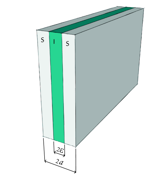
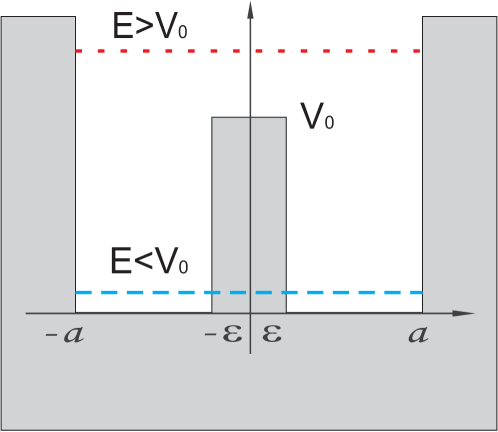
The total thickness of the SIS nanofilm and of the insulating barrier are and , respectively, as depicted in Fig. 1. The insulating slab is a potential barrier of height that acts in the single particle channel of the BdG equations, namely, described by the Hamiltonian of Eq.(8), through the potential that confines particles inside the SIS nanofilm.
| (38) |
Fig. 2 depicts this rectangular barrier of height and two single particle energies, representative of states that lie above and below the barrier. Many properties of the single particle states in presence of the potential barrier can be understood without solving the Schroedinger equation (Eq.(32)). This is because the parity (even-odd) symmetry is broken by the barrier which splits the single particle states into states that are strongly affected by the presence of the barrier and others that are not. The odd states are very little sensitive to the barrier because their wavefunction vanishes inside the barrier. Oppositely, changes in the strength of the barrier severely affect the even states since they dos not vanish inside it. In this paper we work within the approximation that the odd levels are absolutely not affected by the barrier, which means a very thin insulating slab. In this case the potential barrier of the SIS nanofilm can be approximated by a delta function potential Flügge (2013),
| (39) |
We find convenient to describe the insulating barrier through a characteristic wave number, , related to and by the assumption of equivalence of the rectangular barrier area.
| (40) |
The characteristic energy of the discrete levels, caused by the perpendicular confinement is
| (41) |
Then one obtains that,
| (42) |
To get a rough estimate for it, consider , then meV, where must be expressed in nm-1.
The delta function potential description provides a simplified model that retains key features of the barrier. There are single particle states above and below the barrier, such as shown in Fig. 2. The perpendicular discrete levels remain parabolic for any , . We briefly summarize some key properties of the even and odd energy levels within the delta function description of the barrier. Even and odd single energy levels alternate in sequence, as shown in Figs. 3 and 4. The even levels have their wavenumber determined by
| (43) |
where for a given there are several solutions. They are affected by the presence of the insulating barrier, , as previously described. The odd wavenumbers are simply given by
| (44) |
The physical interpretation of is a crossover wavenumber.
It sets the regime beyond which the barrier is no longer felt, thus in agreement with Fig. 2.
To see this notice that Eq.(43) can be written as .
For the eigenvalue equation simply becomes since the trigonometric functions are bounded.
Thus even modes become , . They do not feel the barrier and can be considered as lying above it.
For the eigenvalue equation must be solved and in this case the even modes feel the barrier. In summary is the critical wavenumber associated to the barrier height.
To reach understanding of the effects of the potential barrier into the single particle energy levels, we consider three special values of the potential barrier strength, namely, , finite, and .
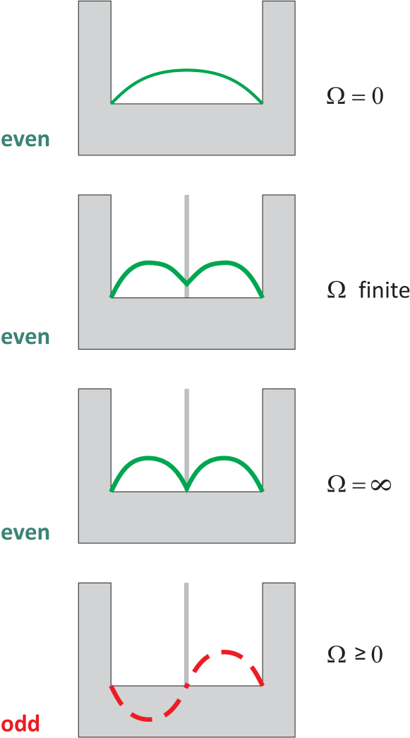
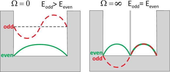
Fig. 3 shows the single particle ground and first excited states, which are even and odd states, respectively.
While the ground state is deformed by the potential barrier, the first excited state remains unaffected.
They are quite distinct for , but as the ground state becomes equal to the ground state, although doubled due to the presence of the infinite barrier.
Moreover the ground and first excited states become equivalent in this limit since even and odd levels coincide apart from a negative phase difference in one of the half-widths.
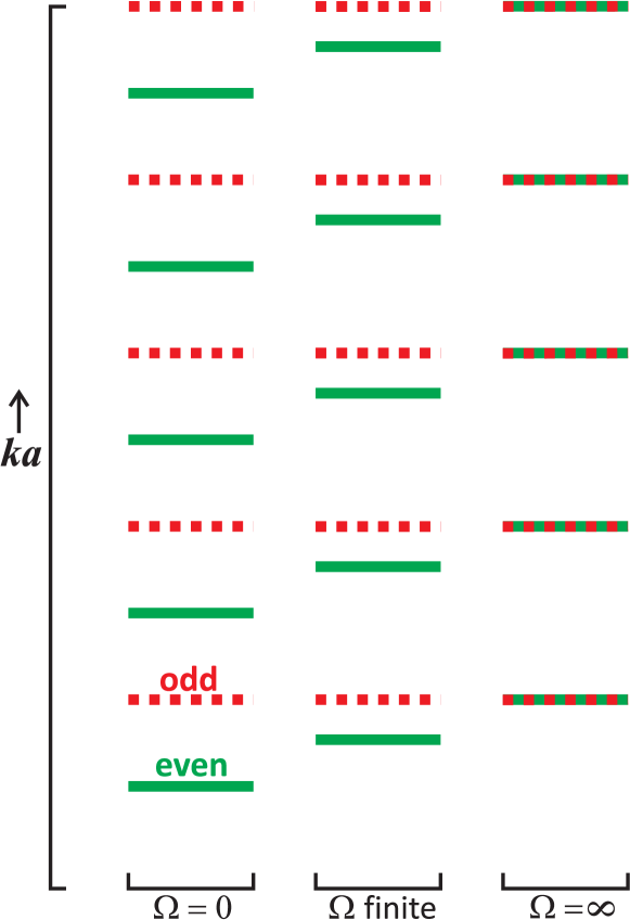
Fig. 4 gives a pictorial view of the discrete levels, as a function of , in these three situations. It also shows that from to even and odd levels approach each other and confirms the degeneracy seen in
Fig. 3 for the fundamental and first excited states here extended for all other even and odd excited levels.
As even and odd levels alternate in energy at the limit they become degenerate in energy.
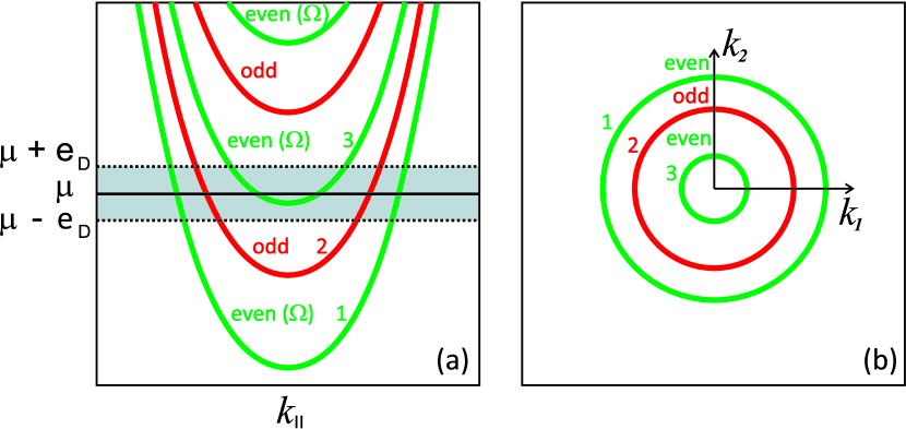
Fig. 5 describes the multiple Fermi surfaces in the nanofilm. The first panel shows the several parabolic bands and their intersection with the Debye energy window defined by Eq.(47). It takes into account the alternate presence of even and odd levels, which is a general property of the SIS nanofilm. The second panel shows the result of the intersection of the parabolic bands with the chemical potential, which at zero temperature is fixed and equal to the three-dimensional Fermi energy of the bulk system,
| (45) |
At zero temperature, the multiple two-dimensional Fermi surfaces are defined by,
| (46) |
Thus even and odd Fermi surfaces succeed in sequence of increasing until a maximum is reached, and beyond which it is no longer possible to have a positive . The crossing of the Debye energy window,
| (47) |
centered at , with these multiple bands, defined by , is shown in Fig. 5. As well-known, pairing occurs only within the Debye energy window around each of these two-dimensional Fermi surfaces.
An interesting feature of the SIS nanofilm is the equivalence of its two extreme limits concerning the barrier strengt: and also should yield the same physics since the single slab nanofilm is retrieved in both limits. For the SIS nanofilm becomes two independent disconnected single slab nanofilms with half the width of the case. However close to a critical value of the barrier, the present BdG formalism and its Anderson approximation break down. This is because the splitting between consecutive even and odd single particle energy levels becomes smaller than the superconducting gap. The present formalism does not contemplate the possibility of pairing between particles in distinct energy levels (cross pairing) and only considers pairing between particles in the same energy level, with the possibility of Cooper pair transfer between different subbands.
IV Multiband and multigap structure of SIS nanofilms
The insulating barrier lifts the degeneracy of even and odd single particle states, because it acts differently on them, rendering the superconducting gap in SIS nanofilm very distinct from the one in single slab nanofilm. Therefore the SIS nanofilm can be regarded as a tunable system to study the interplay between parity symmetry and superconductivity. The SIS and the single slab nanofilms are both multiband systems but with very distinct multigap structure, as shown here. The single slab features multigaps only within the shape resonance region whereas the SIS nanofilm is multigapped independently of any resonance condition.
We assume here that for all the 2D Fermi surface the Debye energy window is the same, similarly to the Thompson-Blatt model for the single slab nanofilm Thompson and Blatt (1963). The effective pairing interaction in the BCS like approximation exists only within the Debye energy window. According to Eq.(29) one obtains that,
| (48) |
where the matrix elements were defined in Eqs.(20) and (34), and is defined in Eq.(30). The Heavyside function, , has been employed: for and for . The superconducting gap is homogeneous within each Debye energy window,
| (49) |
There is a maximum parallel energy and a minimum one, , which defines the parallel energy window, .
| (50) | |||||
| (51) |
Let us analyze this parallel energy window according to the three possible positions of the Debye energy window:
-
1.
is above the bottom of the band. Then and and .
-
2.
touches the bottom of the band, namely, . Then and , thus .
-
3.
is below . Then and , and consequently .
In this paper we take the assumption that . This renders the window very narrow and consequently, also the (shape) resonance window small. We also take that the parallel electronic density of states is constant, and given by the standard definition,
| (52) |
Therefore the summation over single particle states is really given by . The equation that determines the superconducting gaps is obtained by integrating over the parallel momentum:
| (53) | |||
| (54) |
where the interaction matrix has been defined in Eq.(34).
We have expressed the coupling , introduced in Eq.(20), in terms of , previously defined in Table 2:
| (55) |
where is the three-dimensional Fermi wavenumber. Although we do not impose a fixed total number of particles, for the sake of completeness, we show that Eq.(10) becomes,
Next the special limits of no barrier () and of an infinitely strong barrier () are discussed.
They do not yield any novel result, as they reduce to the single slab nanofilm, well described by Thompson and Blatt Thompson and Blatt (1963).
Nevertheless they provide an opportunity to understand properties of the SIS nanofilm and for this reason
we obtain the solutions of Eq.(53) in these two limits.
The single particle states are obtained in the appendices A.3 and A.4 from our general approach.
Fig. 6 depicts for , the single particle ground and the first excited states, which are even and odd states, respectively. This is the single slab nanofilm limit and the interaction matrix (Eq.(34)) becomes , as follows from our general expression of Eq.(C), shown in appendix C. The single particle energies are given by Eqs.(77) and (79) for even and odd levels, respectively. Assume the chemical potential out of a resonance condition, namely the first among the three possibilities previously listed. Away from a shape resonance window Eq.(53) becomes,
| (57) |
There is a maximum quantum level,
| (58) |
where “floor” stands for the lowest integer. This integer is obtained from Eq.(50) and defines the number of activated bands. When all superconducting gaps are equal, , one can easily solve Eq.(57) and find its value,
| (59) |
Indeed this equal superconducting gap solution is found in Thompson and Blatt’s original work Thompson and Blatt (1963).
We also confirm that all superconducting gaps are equal away from resonance from our numerical solution of Eq.(53), which is solved iteratively.
For the single particle states are given by Eq.(81) for both even and odd levels. The analysis of this case is instructive because the two single slab nanofilms limit must be recovered.
Fig. 6 depicts the even and odd single particle wave functions for . Even and odd single particle energies are equal in this limit. The wave functions coincide apart from a phase difference in one of the sides of the barrier (negative sign). This negative sign is irrelevant for the matrix elements of Eq.(20) since they only take into account the modulus of the wave function. According to the general treatment of the matrix elements done in appendix C, even and odd terms are all equal: . Consequently the superconducting gaps can be considered equal away from the shape resonances. In case that the shape resonances are very narrow. Then and one obtains a single equation to describe even and odd gaps,
| (60) |
Recall that we are considering that and the out of resonance condition, the first one among the three possibilities previously discussed for the chemical potential. Then we obtain from Eq.(53) that,
| (61) |
The maximum quantum level is easily obtained from Eq.(50):
| (62) |
Notice that also follows from Eq.(58) under the replacement . Numerical analysis of Eq.(61) shows that all gaps are equal away from the shape resonance, . Under this assumption the superconducting gap can be easily obtained,
| (63) |
In summary the infinite barrier SIS nanofilm () is equivalent to the single slab nanofilm (),
because Eq.(61) is equivalent to Eq.(57) under the replacement .
This replacement also renders Eq.(63) equivalent to Eq.(59).
Next we consider the breaking of the present BdG approach due to the onset of cross pairing. The energy splitting between even and odd states, associated to the same discrete state, in the limit , is
| (64) |
according to Eqs.(81) and (87). Essentially cross pairing must be considered in case the above single particle energy splitting becomes comparable to the bulk gap. We define the critical strength at . The smallest splitting is in the first level, . As an example consider the case of a SIS nanofilm with total thickness 2.0 nm, that is, (see Eq.(41)). Then the critical strength of the barrier is given by,
| (65) |
where is defined in Eq.(41). Recall that the discreteness along the perpendicular direction is based on .
Notice that there are two important electronic energy differences, namely, between even and odd levels that form a pair, and between two consecutive pairs. Even in case the even to odd splitting within a pair falls shorter than the bulk gap, the splitting between the two pairs consecutive pairs remains larger than the bulk gap, and so, justify the discrete treatment in the perpendicular direction. For instance,
| (66) |
Again taking the example of and , gives that .
V Physical parameters and single particle states
We take the parameters of Niobium described in Tables 1 and 2 as a basis for the discussion about the multigap and the interaction driven resonance in SIS nanofilms. We also list the physical parameters of Aluminum and Lead, although the present study does not address nanofilms made of these metals.
The minimum energy needed to break a Cooper pair into two independent electrons is . According to the BCS theory the superconducting gap is related to the critical temperature by and Aluminum, Lead and Niobium satisfy approximately this relation Kittel (1976); Ashcroft and Mermin (1976); Rohlf (1994) as seen in Table 1, which also contains other parameters needed for the study of the SIS nanofilm, such as , E, , and the Fermi wavenumber, .
Table 2 shows the required parameters in units of the Debye energy. The ratio is extensively used in our considerations. Table 2 also contains for the three metals the critical strength of the barrier, defined by Eq.(65). For (see Eq.(41)) the ratio , thus a few discrete energy levels fall below the chemical potential, which means that a few of the two-dimensional Fermi surfaces can develop a superconducting gap. It also holds that the Debye energy is much smaller than the typical quantized energy across the film, . The chemical potential is significantly larger than the Debye energy for the three metals, , which justifies the analysis done in section IV. The dimensionless parameter , defined in Eq.(55), gives the strength of the pairing interaction and is determined from the the requirement that the nanofilm gaps approach the bulk gap in the limit of increasing thickness.
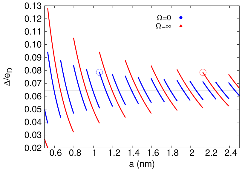
Fig. 7 shows the gap versus the half width in the limits and , as obtained from the single gap solutions of Eqs.(59) and (63). To help visualize the equivalence between the and limits, the points 1.063 nm and 2.126 nm are encircled. They yield the same gap value .
We use the parameters of Niobium previously assigned to describe the SIS nanofilm. The shape resonances correspond to the discontinuities where the gap jumps from below to above its bulk value. The bulk gap value is represented there by a black horizontal line. Indeed Eqs.(59) and (63) do not give a good description near to the shape resonances, where in fact a multigap structure arises. There the gap must be directly obtained from Eqs.(53) and (54). Recall that Eqs.(59) and (63) are approximate solutions of Eqs.(53) and (54) only valid away from resonances.
VI Multigap features of the SIS nanofilm at a shape resonance
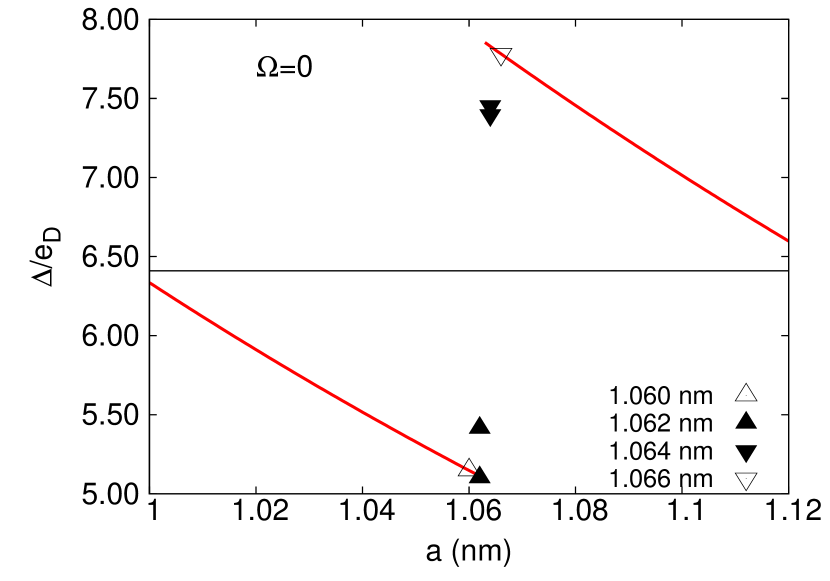
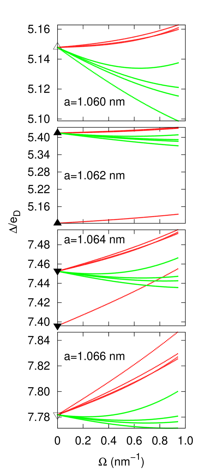
In this section a Nb SIS nanofilm is studied with half width in the range 1.060 to 1.066 nm and a very weak insulating barrier ().
Although the studied window is too small to be physical, the present analysis brings understanding about the fundamental differences between the multigap properties of the SIS and the single slab superconducting nanofilms.
Essentially we show here that the SIS nanofilm is intrinsically multigapped whereas the single slab is not.
Through the shape resonance window one observes the onset and disappearance of multiple gaps in the single slab nanofilm while the SIS nanofilm always remains multigapped.
Fig. 8 shows the gaps in case of no barrier (), as obtained through Eqs.(59) and (53). The first equation gives the continuous (red) lines while the second one is used for specific points in the resonance region, namely 1.060, 1.062, 1.064 and 1.066 nm. Recall that Eq.(59) is obtained under the assumption of just one single gap and away from resonance. Eq.(53) provides a self consistent numerical method to numerically determinate the gaps. Away from resonance they give the same results which proves the righteousness of the gap solution of Eq.(59) for . Indeed the numerical solution of Eq.(53) shows that the cases 1.060 nm and 1.066 nm are the extremities of the shape resonance, as just a single gap is obtained, as shown in Fig. 8. For the intermediate widths, 1.062 nm and 1.064 nm, Eq.(53) gives two gaps corresponding to a change in the number of single particle states below the chemical potential. Thus these two half widths fall in the shape resonance window, since a second gap appears, which corresponds to the entrance of a new band into the Debye energy window. The two gaps at 1.062 and 1.064 nm cannot be described by Eq.(59) since this formula does not account for different gaps. Table 3 shows the single particle energy levels at the extremities of the studied interval and the onset of a new single particle energy state into the Debye energy window. The number of even levels remain unchanged while the odd ones are changed by one. Recall that according to Table 2, .
Next consider the situation of a weak potential barrier, as shown in Fig. 9. The four half widths 1.060, 1.062, 1.064 and 1.066 nm are considered here in case that . They were considered before in Fig. 8 in case that . Some very distinct features are noticeable in the comparison of the extremities ( 1.060 nm, 1.066 nm) with the resonating widths ( 1.062 nm, 1.064 nm). At the extremities, the splitting of the gap is purely due to the barrier since for the gaps have all the same values. Interestingly the parity symmetry for is unbroken in the superconducting properties since even and odd gaps are equal. Nevertheless for this degeneracy is lifted since even and odd gaps are no longer equal. Interestingly just a small potential barrier is enough to do this splitting and unveil the multigap nature of the SIS nanofilm. The interaction splitting is small () in comparison with the shape resonance splitting ().
The even single particle states in the range , are well described by Eq.(86), which is a good approximation to the exact solution of Eq.(43) for a weak insulating barrier range. Fig. 9 shows the gaps obtained by solving Eqs.(53) and (54) with matrix elements Eqs.(89), (b), (c), and (d). The even wavenumbers are obtained from Eq.(87), which provides an approximate solution of Eq.(43).
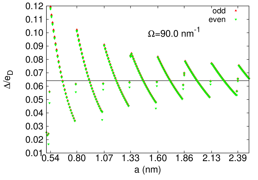
Fig. 10 shows the gaps within the same half width window of Fig. 7, , but for . Its understanding must be complemented by Table 4, which provides further information about the number of gaps and their range. Notice that for the SIS nanofilm the number of distinct gaps is the same as the number of accessible bands. Table 4 shows the critical half widths where there is a change in the number of even and odd bands within the studied range . We conclude from Fig. 10 that shape resonances still exist for finite . Nevertheless the shape resonance acquires a more elaborate structure since the number of even and odd single particle levels, which here is the same as the number of distinct gaps, change in similar but not equal widths. According to Table 4 the tip of the curves in Fig. 10, associated to the highest possible gaps, have an equal number of even and odd single particle states below the chemical potential. At the bottom of these curves, where the lowest gap values of these curves is reached, one observes the increase by one in the number of even single particle states, according to Table 4. Next and within a very close half width value, a new transition takes place where a new odd level is added. Lastly there is a third transition corresponding to the final jump to the top of the next curve where an even level is added. Then even and odd levels become equal again.
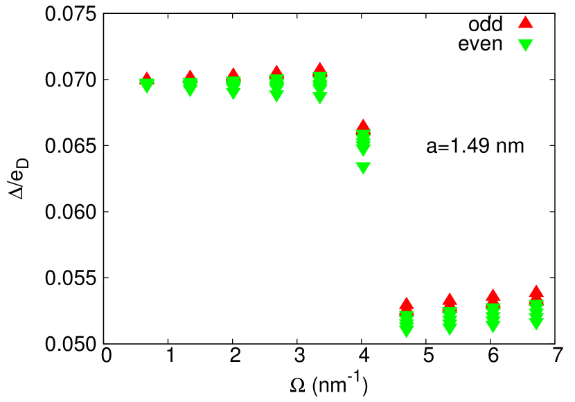
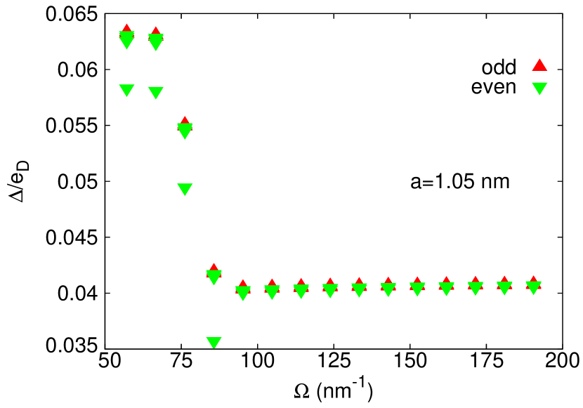
VII Interaction driven resonance
In this section two Nb SIS nanofilms with fixed half widths are studied, namely 1.49 and to 1.05 nm, in different ranges of . The goal is to show the presence of interaction driven resonances which means that the superconducting gaps undergo abrupt changes by adjustment of without changing the half width .
The shape resonance, obtained by tuning of the half width, , affects all discrete states but the interaction resonance can only affect the even states because only them feel the barrier. Therefore the cause of an interaction resonance is the passage of an even single particle state through the Debye energy window that renders a new (even) band accessible for pairing. Fig. 11 and Fig. 12 show the gaps obtained by solving Eqs.(53) and (54) with matrix elements Eqs.(89), (b), (c), and (d). It remains to describe how the wavenumbers of Eq.(43) are obtained. Below we study two examples of interaction driven resonance that take place in distinct ranges of barrier strength.
The first example is for 1.49 nm at a fixed set of ten insulating barrier strengths, given by , whose wavenumbers are listed in Table 5 and correspond to exact solutions of Eq.(43). Notice that in Table 5 the single particle energy level lies above the Debye energy window for any in this table and for this reason does not contribute to the superconducting state. The level falls below (or inside) the Debye energy window from to , and above from to . corresponds to the barrier strength shown in Table 6. The single particle energy level lies below the Debye energy window for any in this table. Within this range of solutions the interaction resonance can also be observed for other half widths in the proximity of 1.49 nm. The interaction resonance moves out of this fixed window for values of significantly different from the above one. Fig. 11 shows the gaps, as obtained from Eq.(53), versus the insulating barrier strength. An abrupt change of the gaps take place near to 4.03 nm-1 which characterizes the interaction resonance. Notice in this figure the multigap structure with odd gaps (triangles, red) above the even gaps (upside triangle, green). Table 6 is complementary to Fig. 11 as it shows at selected values of , the energies of the single particle states through this transition. By increasing the barrier strength the number of single particle states inside and below the Debye energy window changes from 6 to 5. Specific values of were selected to characterize the transition, namely, 3.36 (below), 4.03 (in) and 4.70 (above) nm-1. The odd single particle energy levels are not affected by changes in the barrier strength, as shown in Table 6. Fig. 11 shows that the change in the gap values through the interaction resonance can be quite high ().
The second example is for half width 1.05 nm and takes place at the range of potential barrier strength . In this example the even single particle states are obtained as approximate solutions of Eq.(43) given by Eq.(87). Fig. 12 shows the multigaps versus with significant changes in the gap at the interaction resonance (). The interaction resonance observed at = 85.71 nm-1 also exist in a different but still within the studied range for similar half widths. Notice that the studied range falls below 246 nm-1 (Table 2) beyond which crossing pairing between the even and odd levels must be included, which is not done here. Table 7 shows through three selected values of , 76.19, 85.71 and 95.24 that the number of even single particle states under the chemical potential drops from 4 to 3 in this transition. Nevertheless the number of odd levels remains constant throughout this transition.
| 1.0 | 2.0 | 3.0 | 4.0 | 5.0 | 6.0 | 7.0 | 8.0 | 9.0 | 10.0 | ||
|---|---|---|---|---|---|---|---|---|---|---|---|
| 1 | 3.1416 | 2.02876 | 2.28893 | 2.45564 | 2.57043 | 2.65366 | 2.71646 | 2.76536 | 2.80443 | 2.8363 | 2.86277 |
| 2 | 6.2832 | 4.91318 | 5.08699 | 5.23294 | 5.35403 | 5.45435 | 5.53782 | 5.60777 | 5.66687 | 5.71725 | 5.76056 |
| 3 | 9.4248 | 7.97867 | 8.09616 | 8.20453 | 8.30293 | 8.39135 | 8.47029 | 8.54057 | 8.60307 | 8.6587 | 8.70831 |
| 4 | 12.5664 | 11.0855 | 11.1727 | 11.256 | 11.3348 | 11.4086 | 11.4773 | 11.5408 | 11.5993 | 11.6532 | 11.7027 |
| 5 | 15.7080 | 14.2074 | 14.2764 | 14.3434 | 14.408 | 14.4699 | 14.5288 | 14.5847 | 14.6374 | 14.6869 | 14.7335 |
| 6 | 18.8496 | 17.3364 | 17.3932 | 17.449 | 17.5034 | 17.5562 | 17.6072 | 17.6562 | 17.7032 | 17.7481 | 17.7908 |
| 7 | 21.9911 | 20.4692 | 20.5175 | 20.5652 | 20.612 | 20.6578 | 20.7024 | 20.7458 | 20.7877 | 20.8282 | 20.8672 |
| 1.49 | 3.36 | 4.03 | 4.70 |
| nm | nm-1 | nm-1 | nm-1 |
| symmetry | |||
| even | 5.082 | 5.325 | 5.518 |
| even | 21.47 | 22.13 | 22.69 |
| even | 50.81 | 51.77 | 52.63 |
| even | 93.92 | 95.06 | 96.11 |
| even | 151.1 | 152.3 | 153.5 |
| even | 222.4 | 223.7 | |
| odd | 7.122 | 7.122 | 7.122 |
| odd | 28.49 | 28.49 | 28.49 |
| odd | 64.01 | 64.01 | 64.01 |
| odd | 114.0 | 114.0 | 114.0 |
| odd | 178.1 | 178.1 | 178.1 |
| 1.05 | 76.19 | 85.71 | 95.24 |
| nm | nm-1 | nm-1 | nm-1 |
| symmetry | |||
| even | 13.99 | 14.03 | 15.06 |
| even | 55.96 | 56.11 | 56.23 |
| even | 125.9 | 126.3 | 126.5 |
| even | 223.8 | 224.4 | |
| odd | 14.34 | 14.34 | 14.34 |
| odd | 57.37 | 57.37 | 57.37 |
| odd | 129.1 | 129.1 | 129.1 |
VIII Discussion
The study of nanostructured superconductors is important for many reasons, among them the quest to predict and realize metallic heterostructures that are multiband and multigap and present BCS-BEC crossover from momentum to position space pairing that can be tuned by system parameters. Theoretical and experimental evidences have shown that nanostructuring of bulk superconductors, in the forms of nanofilms, nanostripes, and nanoclusters is able to induce multigap and multiband superconductivity and superconducting shape resonances Perali et al. (1996); Bianconi et al. (1997, 1998); Zhang et al. (2010). Ref. Shanenko et al., 2015 contains an overview of the experimental state of the art for superconducting nanofilms. Multiband and multigap superconductors bring new paradigms to the understanding of coherent quantum phenomena, such as the enhancement of the superconducting critical temperature and the pairing energy gaps Milošević and Perali (2015) through tunable parameters. The BCS-BEC crossover is also a central issue in present studies of high-Tc superconductivity. It has been proposed in Aluminum doped MgB2 Innocenti et al. (2010) through a two-band, two-gap resonant superconductivity model. The BCS-BEC crossover has been studied in two-band and two-gap superconductors Guidini and Perali (2014) and also in quantum confined superconductors and superfluids Guidini et al. (2016); Shanenko et al. (2012). Mostly important for connections with the results of the present work is the prediction that superconducting nanofilms can show BEC (molecule like) pairing induced by quantum confinement when the number of monolayer is reduced to a few units Chen et al. (2012). From the other side the shape resonances in superconducting gaps and critical temperature are expected to be generally present in a quasi two-dimensional electron gas formed at oxide-oxide interface Bianconi et al. (2014), which is another system that could be used to realize the SIS structure investigated in this paper. Finally, we note that the shape resonances in superconducting nanofilms discussed at length in this paper are always accompanied by a topological change in the geometry of the Fermi surfaces, which is a Lifshitz transition. The Lifshitz transitions seem to be a general feature of high-Tc superconductors, in particular in iron-based systems. Key predictions associated with the Lifshitz transitions are resonances and amplifications in the superconducting critical temperature, as recently observed in electron-doped FeSe monolayer Shi et al. (2016) and a typical chemical potential (density) dependence of the superconducting isotope effect in the critical temperature Perali et al. (2012).
IX Conclusion
In this paper we have shown that the presence of an insulating potential barrier between two superconducting slabs in the quantum size regime brings novel and interesting effects not found in the single superconducting slab nanofilm. This is because of the parity symmetry brought into play by the insulating barrier. The single particle states either vanish at the insulating barrier (odd) or not (even). The even states are strongly affected by the insulating barrier whereas the odd ones are not, and this leads to a segregation between even and odd superconducting gaps. Consequently noticeable effects are found in the superconducting properties of the nanofilm, such as intrinsically multigapped superconductivity and interaction driven resonances, the latter being distinct from the well-known Thompson-Blatt shape resonance. The results presented in this paper have been applied to a Nb-I-Nb nanofilm but the conclusions of multigap superconductivity and interaction driven resonances remain valid for other metals as well.
Acknowledgments: We thank Antonio Bianconi, Mihaill Croitoru, Pierbiagio Pieri for useful discussions. We also thank Natascia De Leo, Matteo Fretto and Nicola Pinto for discussions on the possible experimental realizations of SIS nanofilms. Mauro M. Doria acknowledges CNPq support from funding (23079.014992/2015-39). Marco Cariglia acknowledges CNPq support from funding (207007/2014-4). Andrea Perali acknowledges support by the University of Camerino FAR project CESEMN. The authors thank the colleagues involved in the MultiSuper International Network (http://www.multisuper.org) for exchange of ideas and suggestions for this work.
Appendix A Solution for the Schroedinger equation
Consider the one-dimensional Schroedinger equation of Eq.(32) with the potential,
| (69) |
One of the advantages of the delta function potential is that the energy levels are those of a free particle, although the presence of the potential barrier,
| (70) |
There are two families of solutions according to their parity properties.
A.1 Even solutions:
A.2 Odd solutions:
| (76) |
where the wavenumber is given by,
A.3
The even states correspond to the energy levels,
| (77) |
and the eigenstates in the interval are given by
| (78) |
The odd states correspond to the energy levels,
| (79) |
and the eigenstates in the interval are given by
| (80) |
A.4
Both the even states and odd states correspond to the energy levels,
| (81) |
However the eigenstates are slightly different, while for the odd states in the interval correspond to
| (82) |
for the even states is given by,
| (85) |
Appendix B Approximate solutions for
We obtain useful approximated solutions of Eq.(43) valid in the limit of a weak and of a very strong potential barrier.
B.1
B.2
Appendix C Matrix elements
Important to the present discussion is the obtainment of the dimensionless matrix elements defined in Eq.(34), or equivalently,
The matrix element can be generally expressed as
| (88) |
From the above formula we obtain specific matrix elements.
-
(a)
, odd, odd
(89) The strength of the potential barrier does not affect the odd-odd matrix elements.
-
(b)
, even, odd
(90) In both limits, and , the formula above gives the above limit, namely, .
-
(c)
, even
(91) In both limits, and , the formula above gives that .
-
(d)
, , even, even
(92) In both limits, and , the formula above gives that .
References
- Liu et al. (2001) A. Y. Liu, I. I. Mazin, and J. Kortus, Phys. Rev. Lett. 87, 087005 (2001).
- Giubileo et al. (2001) F. Giubileo, D. Roditchev, W. Sacks, R. Lamy, D. X. Thanh, J. Klein, S. Miraglia, D. Fruchart, J. Marcus, and P. Monod, Phys. Rev. Lett. 87, 177008 (2001).
- Giubileo et al. (2002) F. Giubileo, D. Roditchev, W. Sacks, R. Lamy, and J. Klein, EPL (Europhysics Letters) 58, 764 (2002).
- Iavarone et al. (2002) M. Iavarone, G. Karapetrov, A. E. Koshelev, W. K. Kwok, G. W. Crabtree, D. G. Hinks, W. N. Kang, E.-M. Choi, H. J. Kim, H.-J. Kim, and S. I. Lee, Phys. Rev. Lett. 89, 187002 (2002).
- Iavarone et al. (2005) M. Iavarone, R. Di Capua, A. E. Koshelev, W. K. Kwok, F. Chiarella, R. Vaglio, W. N. Kang, E. M. Choi, H. J. Kim, S. I. Lee, A. V. Pogrebnyakov, J. M. Redwing, and X. X. Xi, Phys. Rev. B 71, 214502 (2005).
- Kortus et al. (2001) J. Kortus, I. I. Mazin, K. D. Belashchenko, V. P. Antropov, and L. L. Boyer, Phys. Rev. Lett. 86, 4656 (2001).
- Bianconi et al. (2007) A. Bianconi, M. Filippi, M. Fratini, E. Liarokapis, V. Palmisano, L. N. Saini, and L. Simonelli, “Electron correlation in new materials and nanosystems,” (Springer Netherlands, Dordrecht, 2007) Chap. II.1 Magnesium diboride and the two-band scenario, pp. 93–101.
- Suhl et al. (1959) H. Suhl, B. T. Matthias, and L. R. Walker, Phys. Rev. Lett. 3, 552 (1959).
- Moskalenko et al. (1991) V. A. Moskalenko, M. E. Palistrant, and V. M. Vakalyuk, Soviet Physics Uspekhi 34, 717 (1991).
- Perucchi et al. (2012) A. Perucchi, L. Baldassarre, S. Lupi, B. Joseph, and P. Dore, in Infrared, Millimeter, and Terahertz Waves (IRMMW-THz), 2012 37th International Conference on (2012) pp. 1–3.
- Abdel-Hafiez et al. (2015) M. Abdel-Hafiez, Y.-Y. Zhang, Z.-Y. Cao, C.-G. Duan, G. Karapetrov, V. M. Pudalov, V. A. Vlasenko, A. V. Sadakov, D. A. Knyazev, T. A. Romanova, D. A. Chareev, O. S. Volkova, A. N. Vasiliev, and X.-J. Chen, Phys. Rev. B 91, 165109 (2015).
- Floris et al. (2007) A. Floris, A. Sanna, S. Massidda, and E. K. U. Gross, Phys. Rev. B 75, 054508 (2007).
- Ruby et al. (2015) M. Ruby, B. W. Heinrich, J. I. Pascual, and K. J. Franke, Phys. Rev. Lett. 114, 157001 (2015).
- Guo et al. (2004) Y. Guo, Y.-F. Zhang, X.-Y. Bao, T.-Z. Han, Z. Tang, L.-X. Zhang, W.-G. Zhu, E. G. Wang, Q. Niu, Z. Q. Qiu, J.-F. Jia, Z.-X. Zhao, and Q.-K. Xue, Science 306, 1915 (2004).
- Bao et al. (2005) X.-Y. Bao, Y.-F. Zhang, Y. Wang, J.-F. Jia, Q.-K. Xue, X. C. Xie, and Z.-X. Zhao, Phys. Rev. Lett. 95, 247005 (2005).
- Zhang et al. (2010) T. Zhang, P. Cheng, W.-J. Li, Y.-J. Sun, G. Wang, X.-G. Zhu, K. He, L. Wang, X. Ma, X. Chen, Y. Wang, Y. Liu, H.-Q. Lin, J.-F. Jia, and Q.-K. Xue, Nat Phys 6, 104 (2010).
- Thompson and Blatt (1963) C. Thompson and J. Blatt, Physics Letters 5, 6 (1963).
- Perali et al. (1996) A. Perali, A. Bianconi, A. Lanzara, and N. Saini, Solid State Communications 100, 181 (1996).
- Shanenko and Croitoru (2006) A. A. Shanenko and M. D. Croitoru, Phys. Rev. B 73, 012510 (2006).
- Josephson (1962) B. Josephson, Physics Letters 1, 251 (1962).
- Golubov et al. (2004) A. A. Golubov, M. Y. Kupriyanov, and E. Il’ichev, Rev. Mod. Phys. 76, 411 (2004).
- Kim et al. (2004) J. Kim, V. Chua, G. A. Fiete, H. Nam, A. H. MacDonald, and C.-K. Shih, Nat Phys 8, 464 (2004).
- Serrier-Garcia et al. (2013) L. Serrier-Garcia, J. C. Cuevas, T. Cren, C. Brun, V. Cherkez, F. Debontridder, D. Fokin, F. S. Bergeret, and D. Roditchev, Phys. Rev. Lett. 110, 157003 (2013).
- Valentinis et al. (2016a) D. Valentinis, D. van der Marel, and B. C., arXiv:1601.04927v1 (2016a).
- Valentinis et al. (2016b) D. Valentinis, D. van der Marel, and B. C., arXiv:1601.04521 (2016b).
- Russo et al. (2014) R. Russo, C. Granata, A. Vettoliere, E. Esposito, M. Fretto, N. D. Leo, E. Enrico, and V. Lacquaniti, Superconductor Science and Technology 27, 044028 (2014).
- Flügge (2013) S. Flügge, Practical Quantum Mechanics, classics in mathematics (Springer-Verlag, 2013).
- Kittel (1976) C. Kittel, Introduction to Solid State Physics (John Wiley & Sons, 1976).
- Ashcroft and Mermin (1976) N. Ashcroft and N. Mermin, Solid State Physics, Science: Physics (Saunders College, 1976).
- Rohlf (1994) J. W. Rohlf, Modern Physics from a to z (Wiley, 1994).
- Bianconi et al. (1997) A. Bianconi, A. Valletta, A. Perali, and N. Saini, Solid State Communications 102, 369 (1997).
- Bianconi et al. (1998) A. Bianconi, A. Valletta, A. Perali, and N. L. Saini, Physica C: Superconductivity 296, 269 (1998).
- Shanenko et al. (2015) A. A. Shanenko, J. A. Aguiar, A. Vagov, M. D. Croitoru, and M. V. Milošević, Superconductor Science and Technology 28, 054001 (2015).
- Milošević and Perali (2015) M. V. Milošević and A. Perali, Superconductor Science and Technology 28, 060201 (2015).
- Innocenti et al. (2010) D. Innocenti, N. Poccia, A. Ricci, A. Valletta, S. Caprara, A. Perali, and A. Bianconi, Phys. Rev. B 82, 184528 (2010).
- Guidini and Perali (2014) A. Guidini and A. Perali, Superconductor Science and Technology 27, 124002 (2014).
- Guidini et al. (2016) A. Guidini, L. Flammia, M. V. Milošević, and A. Perali, Journal of Superconductivity and Novel Magnetism 29, 711 (2016).
- Shanenko et al. (2012) A. A. Shanenko, M. D. Croitoru, A. V. Vagov, V. M. Axt, A. Perali, and F. M. Peeters, Phys. Rev. A 86, 033612 (2012).
- Chen et al. (2012) Y. Chen, A. A. Shanenko, A. Perali, and F. M. Peeters, Journal of Physics: Condensed Matter 24, 185701 (2012).
- Bianconi et al. (2014) A. Bianconi, D. Innocenti, A. Valletta, and A. Perali, Journal of Physics: Conference Series 529, 012007 (2014).
- Shi et al. (2016) X. Shi, Z.-Q. Han, X.-L. Peng, R. Richard, T. Qian, X.-X. Wu, M.-W. Qiu, S. C. Wang, J. P. Hu, S. Y.-J., and H. Ding, arXiv:1606.01470 (2016).
- Perali et al. (2012) A. Perali, D. Innocenti, A. Valletta, and A. Bianconi, Superconductor Science and Technology 25, 124002 (2012).