Tamm-Langmuir surface waves
Abstract
In this work we develop a theory of surface electromagnetic waves localized at the interface of periodic metal-dielectric structures. We have shown that the anisotropy of plasma frequency in metal layers lifts the degeneracy of plasma oscillations and opens a series of photonic band gaps. This results in appearance of surface waves with singular density of states – we refer to them as Tamm-Langmuir waves. Such naming is natural since we have found that their properties are very similar to the properties of both bulk Langmuir and surface Tamm waves. Depending on the anisotropy parameters, Tamm-Langmuir waves can be either forward or backward waves. Singular density of states and high sensitivity of the dispersion to the anisotropy of the structure makes Tamm-Langmuir waves very promising for potential applications in nanophotonics and biosensing.
pacs:
42.79.Gn, 73.20.Mf, 73.40.Rw, 78.20.BhI Introduction
Surface electromagnetic waves can propagate along an interface separating two media while being localized in the transverse direction. There are many types of surface waves including surface plasmon polariton (SPP), optical Tamm waves, D’yakonov waves, Bloch surface waves etc.Polo and Lakhtakia (2011); Maier and Atwater (2005); Pitarke et al. (2007); Vinogradov et al. (2010); Iorsh et al. (2011); Yermakov et al. (2015); Xiang et al. (2014); Zapata-Rodriguez et al. (2013); D’yakonov (1988) Localization of surface waves can reach deep subwavelength level of up to 10 nm at the near-infrared range.Choo et al. (2012) High localization is accompanied by strong amplification of evanescent electromagnetic fields. Such functionality makes surface waves relevant for many applications from subwavelength focusing,Yin et al. (2005); Bartal et al. (2009) imagingBarnes et al. (2003); Fang et al. (2005) and high-resolution lithographyLuo and Ishihara (2004) to on-chip signal processing,Tanaka and Tanaka (2003); Nikolajsen et al. (2004); Zia et al. (2006) non-linear optics, sensing, high-performance absorbers,Wu et al. (2011); Chen et al. (2016), photovoltaics,Atwater and Polman (2010) optical trappingMin et al. (2013); Zhao et al. (2016) and manipulation.Rodríguez-Fortuño et al. (2015); Petrov et al. (2016)
For sensing and spectroscopy applications is often needed to modify the emission rate (enhance or inhibit) of emitters (quantum dots, single atoms or molecules, NV-centers etc) placed in the vicinity of a substrate. In this case, the role of surface optical states (surface waves) becomes of the utmost importance. In particular, a modification of spontaneous emission rate due to guided surface mode of isotropic metasurface was analyzed in Ref. [Lunnemann and Koenderink, 2016]. In Refs. [Neogi et al., 2002; Chang et al., 2006; Barthes et al., 2011] it was shown that SPP can substantially increase the rate of spontaneous emission. However, enhancement of spontaneous emission due to SPP has a resonant behavior since density of optical states tends to infinity at the single frequency – the frequency of surface plasmon resonance, where the group velocity of SPP tends to zero. To achieve the broadband enhancement we need surface waves with high density of states in a broad frequency range.
In this work we develop a theory of surface electromagnetic waves with broadband singular density of states, which are supported by periodic metal-dielectric structures with anisotropic conducting layers.111Under the term “metal” we understand any medium with free carriers. It can be plasma, real metal, superconductor, doped semiconductor etc. In the literature structures consisting of alternating layers of isotropic dielectric and hyperbolic metamaterials are called “multi-scale hyperbolic metamaterial” or “photonic hypercrystal”.Golenickij et al. (2013); Zhukovsky et al. (2014); Smolyaninova et al. (2014); Huang and Narimanov (2014); Narimanov (2015, 2014) We show that the broadband singularity of density of states comes as a result of infinite density of bulk plasmons (Langmuir modes) localized in the metallic layers. The anisotropy of these layers lifts the degeneracy of plasma oscillations and opens a series of photonic bands and gaps. Localized surface states analyzed in this work appear in the opened photonic gaps where anisotropic layers exhibit the properties of a hyperbolic medium.Poddubny et al. (2013) We show that the surface waves under consideration inherit the main properties of bulk Langmuir modes.
The paper is organized as follows. In Sec. II we introduce our model and main equations. The analysis of dispersion, field distribution and dissipation of Tamm-Langmuir surface waves is represented in Secs. III and IV. In Sec. V , we propose the scheme of an experiment for the detection of the Tamm-Langmuir surface waves and model it numerically. The results of the work are summarized in Sec. VI.
II model
II.1 Geometry of structure
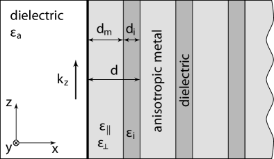
Let us consider a semi-infinite periodic layered structure with a period (Fig. 1). We suppose that the unit cell of the structure consists of two layers. The first one is a dielectric of thickness with constant permittivity . The second one is an anisotropic conducting material with thickness and dielectric function
| (1) |
We suppose that each tensor component depends on the frequency within Drude-Lorentz approximation:
| (2) |
Here, are the plasma frequencies across and along the layers, are the damping frequencies. Therefore, optical axis of anisotropic layers perpendicular to the interface of the structure. Henceforth, we suppose that .
Some natural materials (bismuth,Boyle and Brailsford (1960) graphite,Sun et al. (2011) h-BN Brar et al. (2014)) possess anisotropic plasma frequency. However, the anisotropy can also be induced artificially. For example, in plasma it is achievable via imposing the external magnetic field.Bernstein (1958) In bulk semiconductors it can be accomplished by the implementation of superlattice.Grecu (1973); Koshelev and Bogdanov (2015); Sun et al. (2011); Bogdanov and Suris (2011, 2012) Alternatively, in wire medium, which dielectric function in the GHz frequency region can be described within the Drude approximation, the anisotropy of plasma frequency can be reached due to the difference in the periods along the proper directions.Belov et al. (2003); Silveirinha (2003) The results represented below are scalable and can be applied for different metamaterials operating from the visible to terahertz and radio frequencies (whenever the Drude model is justified).
II.2 Dispersive equation
Let us derive the dispersion equation for surface wave propagating along the interface between a periodic medium and a semiinfinite dielectric cladding. We will seek the solutions of the Maxwell’s equations in the form of TM-polarized wave traveling along the -direction. This means that all field components depend on and as . The electromagnetic field of the surface waves should tend to zero away from the interface, while on the interface the tangential components of electric and magnetic field should be continuous. This condition yields for TM-polarized waves the following dispersion equation:Yeh (1988)
| (3) |
Here, , is the Bloch wave vector, is the permittivity of semiinfinite cladding layer, is a component of the transfer matrix corresponding to single period of the multilayered structure. Yeh (1988) Bloch wave vector in Eq. (3) obeys the dispersion equation for periodic structure
| (4) |
Equations (3) and (4) define the dispersion of the surface waves . The sign of the imaginary parts of wave vector component and Bloch wave vector should be chosen from the condition that electromagnetic field of surface waves tends to zero away from the interface.
In what follows we will use dimensionless quantities:
| (5) |
This means that we measure spatial scale in units of the period.
III Results of calculations
III.1 Isotropic metal-dielectric structure
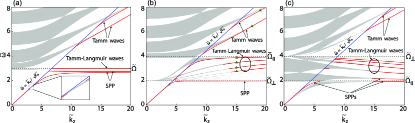
At first, let us analyze the spectrum of the surface waves localized at the interface of an isotropic metal-dielectric structure neglecting the dissipation. This means that and in Eq. (2). The dispersion of surface waves for this case is shown in Fig. 2(a). Dimensionless parameters were taken as follows: , , , , . Gray areas correspond to the allowed photonic bands of the structure. One can see that the spectrum contains two types of surface waves. The waves of the first kind are conventional Tamm waves. Their properties have already been analyzed in detail elsewhere (see, for example, Ref. [Bulgakov et al., 2004]). The frequencies of Tamm waves are above the plasma frequency where metal layers exhibit dielectric behaviour. Therefore, metal-dielectric structure in this case can be considered as a dielectric Bragg reflector.
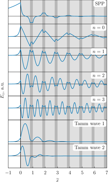
The distribution of electromagnetic field for Tamm waves is shown in Fig. 3. One can see that electromagnetic field oscillates inside the layers and exponentially decreases away from the interface.
Second type of surface wave which can propagate along the interface of isotropic metal-dielectric structure is surface plasmon polariton. Its properties are well-documented in different structures (see, e.g., Ref. [Pitarke et al., 2007]). in Fig. 2(a) we can see two SPP modes: symmetrical and asymmetrical.
The line corresponds to bulk plasmons (Langmuir waves). Langmuir wave represents collective oscillations of free charges. If all charges are identical and do not interact with each other then we have set of unbound oscillators with same eigenfrequency . In this particular case Langmuir modes are actually not waves since their group velocity is zero and they do not transfer energy. If we take into account the interaction between oscillators it results in the appearance of dispersion and non-zero group velocity.Rukhadze and Silin (1961); Forstmann and Gerhardts (1986)
Magnetic field of the Langmuir waves is equal to zero, i.e. these are pure electric waves. The electric field is perfectly confined inside the metal layers. Therefore, metal-dielectric structure represents a set of unbound metal waveguides. Electric field of Langmuir waves can have arbitrary spatial distribution inside the layers but should be equal to zero on the boundaries of the layers. This means that Langmuir modes are infinitely degenerated. However, in reality the degeneration degree is finite due to the spatial dispersion which is generally exist.
III.2 Anisotropic metal-dielectric structure
Let us now analyze the spectrum of the surface waves localized at the interface of an anisotropic metal-dielectric structure neglecting dissipation (). Two cases are possible: (i) ; (ii) . Dispersion of the surface waves for both of these cases is shown in Figs. 2(b) and 2(c). One can see that the degeneracy of Langmuir modes is lifted and the line splits into a set of allowed bands corresponding to different Langmuir modes. All of these bands are squeezed between and , thus their density of states remains singular. In each stop band there is one state corresponding to the surface wave but in Fig. 2 we show only first four modes. Frequency region of the singularity is determined by anisotropy, i.e. by plasma frequencies and . It is worth emphasizing that these modes exist alongside with SPP and surface Tamm waves.
The dispersion for the surface wave under consideration is positive if and negative if . Therefore, these waves can be either forward or backward waves. The same conditions are fulfilled for Langmuir modes in plasma waveguide. The field distribution for these surface waves [see Fig. 3] is similar to the Langmuir modes in the plasma waveguide – electromagnetic field oscillates in the conducting layers and have exponential behavior in dielectric layers.Bogdanov and Suris (2012) It might be asserted that the surface wave under consideration inherits the main properties of Langmuir waves. Therefore, it is quite natural to call them Tamm-Langmuir waves. An important feature is that a single Tamm-Langmuir state always exists between allowed bands corresponding to Langmuir modes.
As we mentioned above, the number of Tamm-Langmuir waves is infinite in our model. In a real system, their number is finite at least due to spatial dispersion at short wavelengths.Koshelev and Bogdanov (2016)
IV Dissipation of Tamm-Langmuir waves
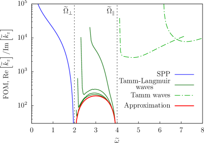
To take into account losses in metallic layer we put in Eq. (2). For the sake of simplicity losses are supposed to be isotropic, i.e. . Figure of merit (FOM) for the surface waves can be introduced as
| (6) |
The meaning of such defined FOM is the free path measured in the wavelength units. So, higher FOM corresponds to smaller losses and bigger propagation length. Figure 4 shows FOM for surface electromagnetic waves for . In the vicinity of the light line () the Tamm-Langmuir modes are weakly localized and their FOM tends to infinity. The same situation is observed for Tamm waves near the cutoffs and for SPP at low frequencies.
Drop of FOM for the Tamm-Langmuir waves near or is explained by the fact that the modes are mainly concentrated in the metal layers where absorption occurs. Analytical expression for the spectrum of FOM can be derived from Eq. (3) under assumption that :
| (7) |
Here, is supposed to be between and . Eq. (7) is plotted in Fig. 4 with red solid line. One can see that it is in good agreement with numerical results for the modes with .
V Simulation of experiment
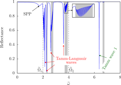
Spectrum of Tamm-Langmuir modes can be analyzed in the experiment where a plane TM-polarized electromagnetic wave impinges onto the interface of a periodic metal-dielectric structure at an angle via a hemispherical high-index dielectric prism coupled to the sample through a thin low-index dielectric layer (Otto configuration).Otto (1968) The scheme of the experiment is shown in the inset of Fig. 6.
As an example, we consider a structure with the parameters from Fig. 2(b). We suppose that the structure consists of 25 periods and is placed on a substrate with permittivity . The prism permittivity is supposed to be equal to 15. The thickness and the permittivity of a dielectric layer separating the prism from the sample are and , respectively.
The reflectance spectrum for the incident angle is shown in Fig. 5. Gray areas mark the allowed photonic bands. The minima in the photonic bandgaps correspond to the excitation of surface waves. Wide dip at low frequencies () corresponds to SPP whereas the dip at high frequencies () is related to the Tamm wave. The series of dips at is a manifestation of Tamm-Langmuir modes.
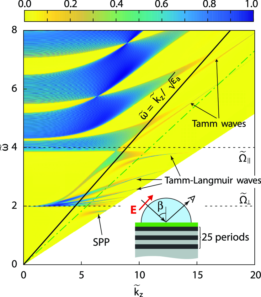
A more full and illustrative picture can be obtained by measuring of the reflection coefficient map – its dependence on both incident angle and frequency (Fig. 6). The comparison of Figs. 6 and 2(b) shows that the reflection coefficient map completely reproduces the numerically calculated spectrum of surface states. The reflection spectrum shown in Fig. 5 corresponds to a section of the reflection coefficient map along the green dot-dashed line. Blue areas correspond to the allowed photonic bands. Since the multilayered structure is a slab with finite thickness, the allowed photonic bands have fine structure. Each of them consists of 25 (number of the periods) tight resonances corresponding to the waveguide modes of the slab.
VI Conclusions
We have shown that the anisotropy of plasma frequency in a periodic metal-dielectric structures lifts the degeneracy of plasma oscillations in the metal layers and opens a series of photonic band gaps. This results in the appearance of surface waves with singular density of states – Tamm-Langmuir waves. Such naming is natural since: (i) their dispersion is very similar to the one of bulk Langmuir modes (bulk plasmons) in hyperbolic metamaterial waveguides (ii) they belong to the photonic band gaps just like Tamm waves. Tamm-Langmuir waves coexist with SPPs and surface Tamm waves. Depending on the anisotropy parameters, Tamm-Langmuir waves can be either forward or backward waves. High density of optical states and low group velocity makes Tamm-Langmuir waves very promising for many applications from nanophotonics to biosensing.
Acknowledgements.
This work has been supported by RFBR (16-37-60064, 15-32-20665), by the President of Russian Federation (MK-6462.2016.2), and by program of Fundamental Research in Nanotechnology and Nanomaterials of the Russian Academy of Science. Numerical simulations have been supported by the Russian Science Foundation (Grant #15-12-20028). The authors are grateful to I. S. Sinev and A. K. Samusev for useful discussions.References
- Polo and Lakhtakia (2011) J. Polo and A. Lakhtakia, Laser Photonics Rev. 5, 234 (2011).
- Maier and Atwater (2005) S. A. Maier and H. A. Atwater, J. Appl. Phys. 98, 011101 (2005).
- Pitarke et al. (2007) J. M. Pitarke, V. M. Silkin, E. V. Chulkov, and P. M. Echenique, Rep. Prog. Phys. 70, 1 (2007).
- Vinogradov et al. (2010) A. P. Vinogradov, A. V. Dorofeenko, A. M. Merzlikin, and A. A. Lisyansky, Phys.-Usp. 53, 243 (2010).
- Iorsh et al. (2011) I. V. Iorsh, A. Orlov, P. Belov, and Y. Kivshar, Appl. Phys. Lett. 99, 151914 (2011).
- Yermakov et al. (2015) O. Y. Yermakov, A. I. Ovcharenko, M. Song, A. A. Bogdanov, I. V. Iorsh, and Y. S. Kivshar, Phys. Rev. B 91, 235423 (2015).
- Xiang et al. (2014) Y. Xiang, J. Guo, X. Dai, S. Wen, and D. Tang, Opt. Express 22, 3054 (2014).
- Zapata-Rodriguez et al. (2013) C. J. Zapata-Rodriguez, J. J. Miret, J. A. Sorni, and S. Vukovic, IEEE J. Sel. Top. Quant. 19, 4601408 (2013).
- D’yakonov (1988) M. D’yakonov, Sov. Phys. JETP 67, 714 (1988).
- Choo et al. (2012) H. Choo, M.-K. Kim, M. Staffaroni, T. J. Seok, J. Bokor, S. Cabrini, P. J. Schuck, M. C. Wu, and E. Yablonovitch, Nat. Photonics 6, 838 (2012).
- Yin et al. (2005) L. Yin, V. K. Vlasko-Vlasov, J. Pearson, J. M. Hiller, J. Hua, U. Welp, D. E. Brown, and C. W. Kimball, Nano Lett. 5, 1399 (2005).
- Bartal et al. (2009) G. Bartal, G. Lerosey, and X. Zhang, Phys. Rev. B 79, 201103 (2009).
- Barnes et al. (2003) W. L. Barnes, A. Dereux, and T. W. Ebbesen, Nature 424, 824 (2003).
- Fang et al. (2005) N. Fang, H. Lee, C. Sun, and X. Zhang, Science 308, 534 (2005).
- Luo and Ishihara (2004) X. Luo and T. Ishihara, Appl. Phys. Lett. 84, 4780 (2004).
- Tanaka and Tanaka (2003) K. Tanaka and M. Tanaka, Appl. Phys. Lett. 82, 1158 (2003).
- Nikolajsen et al. (2004) T. Nikolajsen, K. Leosson, and S. I. Bozhevolnyi, Appl. Phys. Lett. 85 (2004).
- Zia et al. (2006) R. Zia, J. A. Schuller, A. Chandran, and M. L. Brongersma, Mater. Today 9, 20 (2006).
- Wu et al. (2011) C. Wu, B. Neuner, G. Shvets, J. John, A. Milder, B. Zollars, and S. Savoy, Phys. Rev. B 84, 075102 (2011).
- Chen et al. (2016) W.-C. Chen, A. Cardin, M. Koirala, X. Liu, T. Tyler, K. G. West, C. M. Bingham, T. Starr, A. F. Starr, N. M. Jokerst, and W. J. Padilla, Opt. Express 24, 6783 (2016).
- Atwater and Polman (2010) H. A. Atwater and A. Polman, Nat. Mater. 9, 205 (2010).
- Min et al. (2013) C. Min, Z. Shen, J. Shen, Y. Zhang, H. Fang, G. Yuan, L. Du, S. Zhu, T. Lei, and X. Yuan, Nat. Commun. 4, 2891 (2013).
- Zhao et al. (2016) Q. Zhao, C. Guclu, Y. Huang, F. Capolino, R. Ragan, and O. Boyraz, J. Opt. Soc. Am. B 33, 1182 (2016).
- Rodríguez-Fortuño et al. (2015) F. J. Rodríguez-Fortuño, N. Engheta, A. Martínez, and A. V. Zayats, Nat. Commun. 6, 8799 (2015).
- Petrov et al. (2016) M. I. Petrov, S. V. Sukhov, A. A. Bogdanov, A. S. Shalin, and A. Dogariu, Laser Photonics Rev. 122, 116 (2016).
- Lunnemann and Koenderink (2016) P. Lunnemann and A. F. Koenderink, Sci. Rep. 6, 20655 (2016).
- Neogi et al. (2002) A. Neogi, C.-W. Lee, H. O. Everitt, T. Kuroda, A. Tackeuchi, and E. Yablonovitch, Phys. Rev. B 66, 153305 (2002).
- Chang et al. (2006) D. E. Chang, A. S. Sørensen, P. R. Hemmer, and M. D. Lukin, Phys. Rev. Lett. 97, 053002 (2006).
- Barthes et al. (2011) J. Barthes, G. Colas des Francs, A. Bouhelier, J.-C. Weeber, and A. Dereux, Phys. Rev. B 84, 073403 (2011).
- Note (1) Under the term “metal” we understand any medium with free carriers. It can be plasma, real metal, superconductor, doped semiconductor etc.
- Golenickij et al. (2013) K. U. Golenickij, A. A. Bogdanov, and R. A. Suris, in Proceedings 21st International Symposium on ”Nanostructures: Physics and Technology” (St Petersburg, Russia, 2013) p. 315.
- Zhukovsky et al. (2014) S. V. Zhukovsky, A. A. Orlov, V. E. Babicheva, A. V. Lavrinenko, and J. Sipe, Phys. Rev. A 90, 013801 (2014).
- Smolyaninova et al. (2014) V. N. Smolyaninova, B. Yost, D. Lahneman, E. E. Narimanov, and I. I. Smolyaninov, Sci. Rep. 4 (2014).
- Huang and Narimanov (2014) Z. Huang and E. E. Narimanov, Appl. Phys. Lett. 105, 031101 (2014).
- Narimanov (2015) E. E. Narimanov, Faraday Discuss. 178, 45 (2015).
- Narimanov (2014) E. E. Narimanov, Phys. Rev. X 4, 041014 (2014).
- Poddubny et al. (2013) A. Poddubny, I. Iorsh, P. Belov, and Y. Kivshar, Nature Photonics 7, 948 (2013).
- Boyle and Brailsford (1960) W. S. Boyle and A. D. Brailsford, Phys. Rev. 120, 1943 (1960).
- Sun et al. (2011) J. Sun, J. Zhou, B. Li, and F. Kang, Appl. Phys. Lett. 98, 101901 (2011).
- Brar et al. (2014) V. W. Brar, M. S. Jang, M. Sherrott, S. Kim, J. J. Lopez, L. B. Kim, M. Choi, and H. Atwater, Nano Lett. 14, 3876 (2014).
- Bernstein (1958) I. B. Bernstein, Phys. Rev. 109, 10 (1958).
- Grecu (1973) D. Grecu, Phys. Rev. B 8, 1958 (1973).
- Koshelev and Bogdanov (2015) K. L. Koshelev and A. A. Bogdanov, Phys. Rev. B 92, 085305 (2015).
- Bogdanov and Suris (2011) A. A. Bogdanov and R. A. Suris, Phys. Rev. B 83, 125316 (2011).
- Bogdanov and Suris (2012) A. A. Bogdanov and R. A. Suris, JETP Letters 96, 49 (2012).
- Belov et al. (2003) P. A. Belov, R. Marqués, S. I. Maslovski, I. S. Nefedov, M. G. Silveirinha, C. R. Simovski, and S. A. Tretyakov, Phys. Rev. B 67, 113103 (2003).
- Silveirinha (2003) M. G. Silveirinha, Electromagnetic Waves in Artificial Media with Application to Lens Antennas, Ph.D. thesis, Technical University of Lisbon (2003).
- Yeh (1988) P. Yeh, Optical Waves in Layered Media (Wiley, New York, 1988).
- Bulgakov et al. (2004) A. A. Bulgakov, A. V. Meriutz, and E. A. Ol’khovskii, Tech. Phys. 49, 1349 (2004).
- Rukhadze and Silin (1961) A. A. Rukhadze and V. P. Silin, Sov. Phys. Uspekhi 4, 459 (1961).
- Forstmann and Gerhardts (1986) F. Forstmann and R. R. Gerhardts, in Advances in Solid State Physics, Vol. 109 (Springer Berlin Heidelberg, Berlin, Heidelberg, 1986) pp. 291–323.
- Koshelev and Bogdanov (2016) K. L. Koshelev and A. A. Bogdanov, arXiv preprint arXiv:1604.06925 (2016).
- Otto (1968) A. Otto, Z. Phys. 216, 398 (1968).