Crystalline and electronic structure of single-layer TaS2
Abstract
Single-layer TaS2 is epitaxially grown on Au(111) substrates. The resulting two-dimensional crystals adopt the 1H polymorph. The electronic structure is determined by angle-resolved photoemission spectroscopy and found to be in excellent agreement with density functional theory calculations. The single layer TaS2 is found to be strongly n-doped, with a carrier concentration of extra electrons per unit cell. No superconducting or charge density wave state is observed by scanning tunneling microscopy at temperatures down to 4.7 K.
pacs:
73.22.-f,73.20.At,79.60.-iSingle layer (SL) transition metal dichalcogenides (TMDCs) share many fascinating properties with graphene. The electronic properties of the SL differ in subtle but important ways from those of the parent compounds Bollinger et al. (2001); Mak et al. (2010); Splendiani et al. (2010); Novoselov et al. (2005). Most recent research on SL TMDCs has focused on semiconducting materials, because of the possibility to exploit spin and valley degrees of freedom Xu et al. (2014).
Metallic SL TMDCs are interesting for other reasons: Their quasi-2D parent compounds host a wide range of symmetry-breaking electronic instabilities, such as charge density waves (CDWs), superconductivity (SC), and Mott states Wilson and Yoffe (1969); Rossnagel (2011), and it is an open question how these would change in the SL limit. For CDWs driven by electronic correlations or nesting, one might expect an increased transition temperature in the SL limit; but, since the CDW physics in the bulk is often complex, the opposite effect could occur, or an altogether different CDW periodicity might be found. This has been explored theoretically Calandra et al. (2009); Ge and Liu (2012); Laverock et al. (2013); Darancet et al. (2014) and, very recently, experimentally for SL NbSe2 Xi et al. (2015); Ugeda et al. (2016). In SL NbSe2, a strongly increased CDW transition temperature has been observed by optical techniques Xi et al. (2015), whereas atomically resolved scanning tunnelling microscopy (STM) measurements reveal a similar transition temperature as in the bulk Ugeda et al. (2016). Such discrepancies might have several reasons. One is the possible role of contaminations in studies that are not performed in ultra-high vacuum (UHV). Another is the role of the substrate (silicon oxide in case of Ref. Xi et al. (2015) and bilayer graphene in Ref. Ugeda et al. (2016)). For semiconducting TMDCs, the substrate can strongly modify the size of the SL TMDC’s band gap via screening Ugeda et al. (2014); Čabo et al. (2015). This is probably less important for metallic TMDCs but the substrate can still give rise to doping and strain, two factors that significantly influence the formation of CDWs Friend and Yoffe (1987); Soumyanarayanan et al. (2013).
A major challenge in the study of thin TaS2 and other metallic TMDCs is sample preparation. In contrast with some other TMDCs, the material is air-sensitive—particularly in the atomically thin limit Navarro-Moratalla et al. (2016)—and is therefore difficult to prepare by exfoliation. Studies have been carried out on TaS2 flakes exfoliated in air or in glove boxes Navarro-Moratalla et al. (2016); Cao et al. (2014); Galvis et al. (2014), and on flakes isolated by intercalation Ayari et al. (2007), with results that have been partly contradictory, in particular for the case of very thin films.
We overcome the reactivity issue by epitaxially growing SL TaS2 on Au(111) under UHV conditions. This allows for the preparation of atomically clean samples, along with a precise control of layer thickness. Additionally, it results in a well-defined crystalline orientation in the TaS2 with respect to the orientation of the underlying Au(111) substrate. One question that arises is which of two possible structural phases—trigonal prismatic (hereafter referred to as “1H”) or octahedral (“1T”)—will be adopted by SL TaS2 (see insets in Fig. 3). This distinction is important, since the electronic properties and electronic instabilities of the 2H and 1T bulk analogs are entirely distinct from one another Wilson and Yoffe (1969); Rossnagel (2011). A critical question is whether the electronic instabilities observed in the bulk will also occur in the SL Darancet et al. (2014). We find that it is the 1H phase that is adopted in SL TaS2 on Au(111) and that, surprisingly, neither CDW nor SC states are observable at temperatures as low as 4.7 K.
The samples were synthesized using methods that are well-established for the growth of semiconducting SL TMDCs such as MoS2 and WS2; these methods are essentially based on the evaporation of a transition metal in an atmosphere of H2S onto a clean Au(111) surface that had been sputtered and annealed to exhibit the regular herringbone reconstruction Miwa et al. (2015); Grønborg et al. (2015); Dendzik et al. (2015); Martinez et al. (2016). Samples were grown and analyzed in situ with angle-resolved photoemission spectroscopy (ARPES), low-energy electron diffraction (LEED), and STM at the SGM3 end-station of the ASTRID2 synchrotron radiation facility Hoffmann et al. (2004). The sample temperature was 95 K for ARPES and LEED measurements. Low-temperature STM and scanning tunneling spectroscopy (STS) measurements were performed at 4.7 K in a separate chamber, to which the samples were transferred without breaking vacuum.
Density functional theory (DFT) calculations for free-standing SL TaS2 were performed using the VASP code Kresse and Hafner (1993); Kresse and Furthmüller (1996); Kresse (1996). The valence electrons were described by plane-wave basis sets with a kinetic energy threshold of 415 eV. The interaction between the valence and frozen core-electrons was accounted for by means of the projector augmented wave method Blöchl (1994). The Perdew-Burke-Ernzerhof (PBE) approximation to the exchange-correlation functional was used Perdew et al. (1996). The optimized lattice parameter for the 1H and 1T phases of SL TaS2 was found to be 3.337 and 3.372 Å, respectively. The TaS2 SLs were modeled by single (11) unit cells and the reciprocal space was sampled with a (20201) mesh of -points. Electron density was self-consistently converged with an energy threshold of eV. Atomic positions were relaxed until the forces on all atoms were smaller than 0.01 eVÅ-1. Spin-orbit coupling has been taken into account for all calculations.
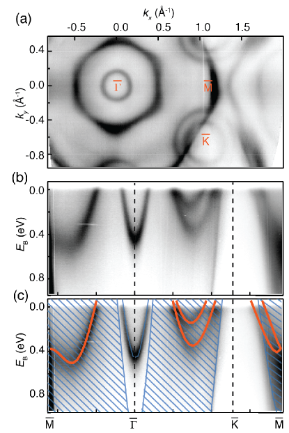
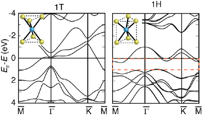
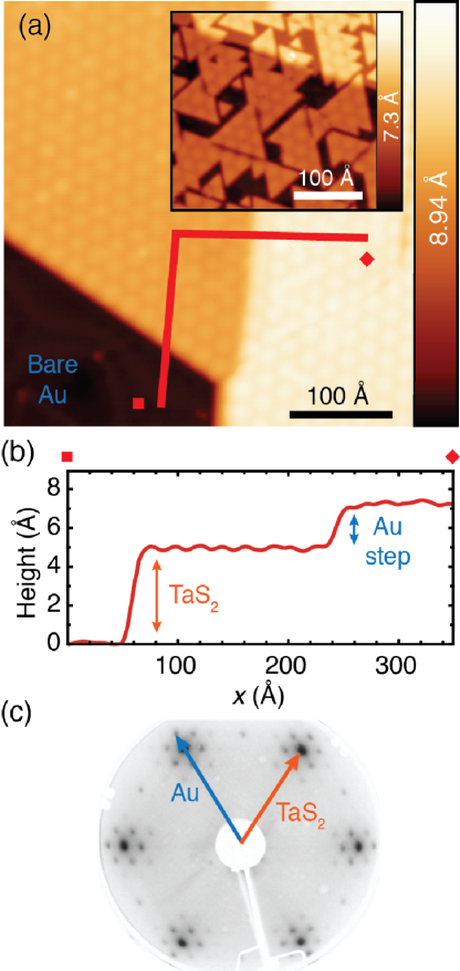
Fig. 1(a) shows the morphology of SL TaS2 measured by STM for two samples of sub-monolayer coverage. For the main panel, the growth conditions have been chosen such as to produce large islands, whereas the inset shows conditions that give rise to many smaller and triangular clusters. The large-scale hexagonal structure visible on the islands in Fig. 1(a) is caused by a moiré superstructure, similar to that observed for MoS2/Au(111) Grønborg et al. (2015) and WS2/Au(111) Dendzik et al. (2015), with a superstructure lattice constant of Å. The moiré’s structure is more clearly seen in the atomically resolved STM image in Fig. 4(a), and leads to satellite spots in the LEED image of Fig. 1(c). LEED and STM results consistently give an in-plane atomic lattice constant of Å for the TaS2 layer, which is the same as in the bulk compounds Wilson and Yoffe (1969).
Note that it is difficult to distinguish between the 1H and 1T phases from such data, since both phases have hexagonal structures with similar lattice constants Qiao et al. (2007). It is evident from the LEED pattern that the TaS2 overlayer possesses a well-defined orientation with respect to the underlying substrate. This orientation still permits the existence of two rotational domains (rotated by 180∘ with respect to each other). The up-pointing and down-pointing triangles in the inset to Fig. 1(a) are distinguished by these two orientations Lauritsen et al. (2007).
Although non-trivial interaction between the TaS2 and the Au(111) is suggested by the well-defined crystalline orientation of the overlayer relative to the substrate, triangular islands are nevertheless observed to readily cross step edges, as in the inset to Fig. 1(a). This growth mode has been identified previously in graphene on certain substrates, such as Ir(111) Coraux et al. (2008), and has been interpreted as a consequence of weak substrate-overlayer interaction.
The ARPES data in Fig. 2 reveal the electronic band structure close to the Fermi level. In addition to the features arising from the exposed Au substrate (in particular, the Au surface state at and the Au sp states closer to the edge of the Brillouin zone (BZ)), the TaS2 overlayer exhibits a Fermi contour (Fig. 2(a)) consisting of two distinct features. The first is an apparently hexagonal contour around the BZ centre . The second consists of two concentric rings around the point.
The structure of the SL, 1H or 1T, can readily be determined by comparison to the DFT calculations for free-standing SL TaS2 shown in Fig. 3. While both the 1H and 1T structures give rise to a metallic SL, the actual band structures are very different. Clearly, the band structure for the 1H modification gives better agreement with the experimental data because it contains the same Fermi contour features, while the Fermi contour for the 1T phase is very different SMA . Indeed, even quantitative agreement can be obtained when the calculated bands are shifted by eV to higher binding energy to account for electron doping. This is shown in Fig. 2(c) (c.f. the region enclosed with a dashed orange box in Fig. 3), where the shifted calculated bands are superimposed on the data. Thus, the structural phase preferred by epitaxial TaS2 on Au(111) is 1H, rather than 1T. As can be seen by inspection of the calculated 1H band structure in Fig. 3, the features at the Fermi surface stem from the same band, which is spin-degenerate near but strongly split near . An inspection of the dispersion along different high-symmetry directions of the BZ (Figs. 2(b) and 3) shows that all Fermi contour features are hole pockets. A comparison to the calculated Fermi contour SMA reveals that the finite but unresolved splitting of the bands near the Fermi contour around is responsible for the apparently hexagonal shape of this hole pocket, even though the individual bands do not have hexagonal Fermi contours.
While the band structure of the bulk 2H parent compound can be considered to be quasi-2D, the truly 2D situation in the SL manifests important differences from the quasi-2D bulk case. Particularly relevant are the modifications to the single band forming the Fermi contour of the SL. In the SL, the band is two-fold degenerate near and spin-split near . In the 2H bulk, on the other hand, the spin degeneracy is never lifted because of the structure’s inversion symmetry. Still, the interaction of the two layers in the unit cell splits the band into two two-fold degenerate bands near while it remains four-fold degenerate at the BZ border point H. This causes a rather strong dispersion perpendicular to the TaS2 layers, giving rise to a deviation from 2D behaviour Barnett et al. (2006). Naively, one might thus expect a stronger tendency for the formation of CDW states in the SL, at least for nesting-driven CDWs.
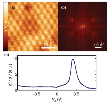
We address the question of whether the sample exhibits CDW or SC by inspecting STM/STS data taken at 4.7 K. In bulk 2H-TaS2, the superconducting critical temperature is = 600 mK Garoche et al. (1978), and a CDW of periodicity sets in below =75 K Wilson and Yoffe (1969), with an accompanying lattice distortion that is clearly visible as a periodic superstructure in the STM data Guillamón et al. (2011) (the same is true for SL NbSe2 Ugeda et al. (2016)). The low-temperature STM data in Fig. 4(a), on the other hand, show no indication of any additional periodicities apart from the lattice as such and the moiré superstructure. This is confirmed by an inspection of the Fourier transformation of the image, which only shows these two periodicities (see Fig. 4(b)). STS measurements made at 4.7 K show a strong feature at approximately 430 meV above the Fermi energy, consistent with results obtained from NbSe2, where this has been associated with the top of the valence band at Ugeda et al. (2016)). The spectra give no indications of a SC gap.
It is not surprising that SC is not observed, since the =600 mK is much lower than the measurement temperatures used in the present study. One set of recent studies has suggested that in thin flakes might be higher than the bulk value Galvis et al. (2014); Navarro-Moratalla et al. (2016)—in contrast to what has been seen for the case of NbSe2, where is suppressed in the SL limit Xi et al. (2015); Ugeda et al. (2016)—but even the highest proposed temperatures for thin TaS2 are considerably smaller than the measurement temperatures of the present study.
The absence of a CDW, however, is surprising. The onset of CDW instability at 75 K in bulk 2H-TaS2, though it is below the temperature at which ARPES and LEED data were collected here, is significantly above that at which STM and STS data were acquired. In the related material NbSe2, there have been conflicting findings for the CDW onset temperature in the SL with respect to the bulk. A strongly increased was reported for SL NbSe2 on silicon oxide Xi et al. (2015), whereas a minor decrease was observed for SL NbSe2 in UHV on bilayer graphene Ugeda et al. (2016).)
In this context, it is interesting to compare the Fermi vector =0.96(2) Å-1 measured across the hole pocket at in the present study with that which would be required if a CDW state were driven by nesting: in the nesting-driven case, the nesting vector would need to be 0.73 Å-1. Clearly, this value matches poorly to the experimentally derived value of ; however, this disagreement is not sufficient to explain the absence of a CDW, since simple nesting cannot explain the CDW in the bulk parent materials, either Rice and Scott (1975); Castro Neto (2001); Rossnagel et al. (2001); Calandra et al. (2009).
The most likely explanation for the lack of CDWs is doping of the TaS2 by the Au substrate. As already seen in Fig. 2(c), the calculated bands have to be shifted to higher energy by 0.12 eV to match the observed dispersion, suggesting that the SL is electron-doped. A rigorous determination of the Fermi contour areas gives a carrier concentration of approximately extra electrons per unit cell SMA —i.e., an occupation of electrons in the uppermost valence band, in contrast with the single electron that one would expect for the undoped material. Previous studies of alkali-intercalation compounds Friend and Yoffe (1987) have shown that the CDW can already be suppressed at more modest electron doping, suggesting that this plays a decisive role.
The CDW transition might also be influenced by other factors: e.g., reduced dimensionality; substrate interactions other than doping, such as screening Ugeda et al. (2014); Čabo et al. (2015); chemical bonding Dendzik et al. (2015); or strain Soumyanarayanan et al. (2013). In the present case, the uncertainty the measurement of the atomic lattice puts an upper limit of 3% on the in-plane strain and Figs. 2 and 3 show that the substrate has only a minor influence on the band structure of SL TaS2, apart from the doping. However, these factors might still play a minor role in suppressing CDW formation Ge and Liu (2012).
In summary, we have successfully used an epitaxial approach to fabricate monolayer TaS2 on Au(111) substrates. We have investigated band structure and crystallinity in situ using ARPES, STM and LEED. We have used low-temperature STM/STS to obtain detailed information on the growth mode and to measure the density of states close to the Fermi level. Comparing our band structure measurements to calculations by DFT, we have determined that our samples are in the 1H phase. We do not see evidence of SC or a CDW state at temperatures down to 4.7 K. It remains, of course, possible that CDW or SC transitions are observed at lower temperatures.
We gratefully acknowledge financial support from the VILLUM foundation, the Danish Council for Independent Research, Natural Sciences under the Sapere Aude program (Grant Nos. DFF-4002-00029, and 0602-02566B), the Lundbeck Foundation. AB acknowledges support from the European Research Council under the European Union’s Seventh Framework Programme (FP/2007-2013) / Marie Curie Actions / Grant no. 626764 (Nano-DeSign). AE and AAK acknowledge financial support from the Emmy Noether Program (KH324/1-1) via the Deutsche Forschungsgemeinschaft, and from FOM which is part of NWO, and the NWO Vidi program.
References
- Novoselov et al. (2005) K. S. Novoselov, D. Jiang, F. Schedin, T. J. Booth, V. V. Khotkevich, S. V. Morozov, and A. K. Geim, Proceedings of the National Academy of Sciences of the United States of America 102, 10451 (2005), URL http://www.pnas.org/content/102/30/10451.abstract.
- Bollinger et al. (2001) M. V. Bollinger, J. V. Lauritsen, K. W. Jacobsen, J. K. Nørskov, S. Helveg, and F. Besenbacher, Physical Review Letters 87, 196803 (2001), URL http://journals.aps.org/prl/abstract/10.1103/PhysRevLett.87.196803.
- Mak et al. (2010) K. F. Mak, C. Lee, J. Hone, J. Shan, and T. F. Heinz, Phys. Rev. Lett. 105, 136805 (2010), URL http://link.aps.org/doi/10.1103/PhysRevLett.105.136805.
- Splendiani et al. (2010) A. Splendiani, L. Sun, Y. Zhang, T. Li, J. Kim, C.-Y. Chim, G. Galli, and F. Wang, Nano Letters 10, 1271 (2010), URL http://dx.doi.org/10.1021/nl903868w.
- Xu et al. (2014) X. Xu, W. Yao, D. Xiao, and T. F. Heinz, Nat Phys 10, 343 (2014), URL http://dx.doi.org/10.1038/nphys2942.
- Wilson and Yoffe (1969) J. A. Wilson and A. D. Yoffe, Advances in Physics 18, 193 (1969), URL http://dx.doi.org/10.1080/00018736900101307.
- Rossnagel (2011) K. Rossnagel, Journal of Physics: Condensed Matter 23, 213001 (2011), URL http://stacks.iop.org/0953-8984/23/i=21/a=213001.
- Calandra et al. (2009) M. Calandra, I. I. Mazin, and F. Mauri, Phys. Rev. B 80, 241108 (2009), URL http://link.aps.org/doi/10.1103/PhysRevB.80.241108.
- Ge and Liu (2012) Y. Ge and A. Y. Liu, Phys. Rev. B 86, 104101 (2012), URL http://link.aps.org/doi/10.1103/PhysRevB.86.104101.
- Laverock et al. (2013) J. Laverock, D. Newby, E. Abreu, R. Averitt, K. E. Smith, R. P. Singh, G. Balakrishnan, J. Adell, and T. Balasubramanian, Phys. Rev. B 88, 035108 (2013), URL http://link.aps.org/doi/10.1103/PhysRevB.88.035108.
- Darancet et al. (2014) P. Darancet, A. J. Millis, and C. A. Marianetti, Phys. Rev. B 90, 045134 (2014), URL http://link.aps.org/doi/10.1103/PhysRevB.90.045134.
- Xi et al. (2015) X. Xi, L. Zhao, Z. Wang, H. Berger, L. Forró, J. Shan, and K. F. Mak, Nature Nanotechnology 10, 765 (2015), URL http://www.nature.com/doifinder/10.1038/nnano.2015.143.
- Ugeda et al. (2016) M. M. Ugeda, A. J. Bradley, Y. Zhang, S. Onishi, Y. Chen, W. Ruan, C. Ojeda-Aristizabal, H. Ryu, M. T. Edmonds, H.-Z. Tsai, et al., Nature Physics 12, 92 (2016), URL http://dx.doi.org/10.1038/nphys3527.
- Ugeda et al. (2014) M. M. Ugeda, A. J. Bradley, S.-F. Shi, F. H. da Jornada, Y. Zhang, D. Y. Qiu, W. Ruan, S.-K. Mo, Z. Hussain, Z.-X. Shen, et al., Nat Mater 13, 1091 (2014), URL http://dx.doi.org/10.1038/nmat4061.
- Čabo et al. (2015) A. G. Čabo, J. A. Miwa, S. S. G. nborg, J. M. Riley, J. C. Johannsen, C. Cacho, O. Alexander, R. T. Chapman, E. Springate, M. Grioni, et al., Nano Letters 15, 5883 (2015), URL http://pubs.acs.org/doi/10.1021/acs.nanolett.5b01967.
- Friend and Yoffe (1987) R. Friend and A. Yoffe, Advances in Physics 36, 1 (1987), URL http://www.tandfonline.com/doi/abs/10.1080/00018738700101951.
- Soumyanarayanan et al. (2013) A. Soumyanarayanan, M. M. Yee, Y. He, J. van Wezel, D. J. Rahn, K. Rossnagel, E. W. Hudson, M. R. Norman, and J. E. Hoffman, Proceedings of the National Academy of Sciences 110, 1623 (2013), URL http://www.pnas.org/content/110/5/1623.abstract.
- Navarro-Moratalla et al. (2016) E. Navarro-Moratalla, J. O. Island, S. Mañas-Valero, E. Pinilla-Cienfuegos, A. Castellanos-Gomez, J. Quereda, G. Rubio-Bollinger, L. Chirolli, J. A. Silva-Guillén, N. Agraït, et al., Nature Communications 7, 11043 (2016), URL http://www.nature.com/doifinder/10.1038/ncomms11043.
- Cao et al. (2014) Y.-F. Cao, K.-M. Cai, L.-J. Li, W.-J. Lu, Y.-P. Sun, and K.-Y. Wang, Chinese Physics Letters 31, 77203 (2014), URL http://iopscience.iop.org/article/10.1088/0256-307X/31/7/077203/meta.
- Galvis et al. (2014) J. A. Galvis, L. Chirolli, I. Guillamón, S. Vieira, E. Navarro-Moratalla, E. Coronado, H. Suderow, and F. Guinea, Phys. Rev. B 89, 224512 (2014), URL http://link.aps.org/doi/10.1103/PhysRevB.89.224512.
- Ayari et al. (2007) A. Ayari, E. Cobas, O. Ogundadegbe, and M. S. Fuhrer, Journal of Applied Physics 101, 014507 (2007), URL http://link.aip.org/link/?JAP/101/014507/1.
- Miwa et al. (2015) J. A. Miwa, S. Ulstrup, S. G. Sørensen, M. Dendzik, A. G. Čabo, M. Bianchi, J. V. Lauritsen, and P. Hofmann, Phys. Rev. Lett. 114, 046802 (2015), URL http://link.aps.org/doi/10.1103/PhysRevLett.114.046802.
- Grønborg et al. (2015) S. S. Grønborg, S. Ulstrup, M. Bianchi, M. Dendzik, C. E. Sanders, J. V. Lauritsen, P. Hofmann, and J. A. Miwa, Langmuir 31, 9700 (2015), URL http://pubs.acs.org/doi/10.1021/acs.langmuir.5b02533.
- Dendzik et al. (2015) M. Dendzik, M. Michiardi, C. Sanders, M. Bianchi, J. A. Miwa, S. S. Grønborg, J. V. Lauritsen, A. Bruix, B. Hammer, and P. Hofmann, Physical Review B 92, 245442 (2015), URL http://journals.aps.org/prb/pdf/10.1103/PhysRevB.92.245442.
- Martinez et al. (2016) J. Martinez, M. Gomez, M. Valentin, E. Preciado, V. Klee, A. Nguyen, A. Berges, D. Lu, M. Isarraraz, and L. Bartels, in Bulletin of the American Physical Society (2016).
- Hoffmann et al. (2004) S. V. Hoffmann, C. Søndergaard, C. Schultz, Z. Li, and P. Hofmann, Nuclear Instruments and Methods in Physics Research, A 523, 441 (2004), URL http://www.sciencedirect.com/science/article/pii/S0168900204000695.
- Kresse and Hafner (1993) G. Kresse and J. Hafner, Physical Review B 47, 558 (1993), ISSN 0163-1829, URL http://link.aps.org/doi/10.1103/PhysRevB.47.558.
- Kresse and Furthmüller (1996) G. Kresse and J. Furthmüller, Computational Materials Science 6, 15 (1996), ISSN 09270256, URL http://www.sciencedirect.com/science/article/pii/0927025696000080.
- Kresse (1996) G. Kresse, Physical Review B 54, 11169 (1996), ISSN 0163-1829, URL http://link.aps.org/doi/10.1103/PhysRevB.54.11169.
- Blöchl (1994) P. E. Blöchl, Physical Review B 50, 17953 (1994), ISSN 0163-1829, URL http://link.aps.org/doi/10.1103/PhysRevB.50.17953.
- Perdew et al. (1996) J. Perdew, K. Burke, and M. Ernzerhof, Physical Review Letters 77, 3865 (1996), ISSN 1079-7114, URL http://www.ncbi.nlm.nih.gov/pubmed/10062328.
- Takeuchi et al. (1991) N. Takeuchi, C. T. Chan, and K. M. Ho, Physical Review B 43, 13899 (1991), URL http://journals.aps.org/prb/pdf/10.1103/PhysRevB.43.13899.
- Qiao et al. (2007) Y.-B. Qiao, Y.-L. Li, G.-H. Zhong, Z. Zeng, and X.-Y. Qin, Chinese Physics 16, 3809 (2007), URL http://theory.issp.ac.cn/publication/2006-2009/qiao07a.pdf.
- Lauritsen et al. (2007) J. V. Lauritsen, J. Kibsgaard, S. Helveg, H. Topsoe, B. S. Clausen, E. Laegsgaard, and F. Besenbacher, Nature Nanotechnology 2, 53 (2007), URL http://dx.doi.org/10.1038/nnano.2006.171.
- Coraux et al. (2008) J. Coraux, A. T. N’Diaye, C. Busse, and T. Michely, Nano Letters 8, 565 (2008), URL http://pubs.acs.org/doi/pdfplus/10.1021/nl0728874.
- (36) See Supplemental Material for information on the determination of the electron doping and the calculated Fermi contours.
- Barnett et al. (2006) R. L. Barnett, A. Polkovnikov, E. Demler, W.-G. Yin, and W. Ku, Phys. Rev. Lett. 96, 026406 (2006), URL http://link.aps.org/doi/10.1103/PhysRevLett.96.026406.
- Guillamón et al. (2011) I. Guillamón, H. Suderow, J. G. Rodrigo, S. Vieira, P. Rodière, L. Cario, E. Navarro-Moratalla, C. Martí-Gastaldo, and E. Coronado, New Journal of Physics 13, 103020 (2011), URL http://stacks.iop.org/1367-2630/13/i=10/a=103020.
- Garoche et al. (1978) P. Garoche, P. Manuel, J. J. Veyssié, and P. Molinié, Journal of Low Temperature Physics 30, 323 (1978), URL http://link.springer.com/article/10.1007/BF00114956.
- Rice and Scott (1975) T. M. Rice and G. K. Scott, Physical Review Letters 35, 120 (1975), URL http://journals.aps.org/prl/abstract/10.1103/PhysRevLett.35.120.
- Castro Neto (2001) A. H. Castro Neto, Phys. Rev. Lett. 86, 4382 (2001), URL http://link.aps.org/doi/10.1103/PhysRevLett.86.4382.
- Rossnagel et al. (2001) K. Rossnagel, O. Seifarth, L. Kipp, M. Skibowski, D. Voß, P. Krüger, A. Mazur, and J. Pollmann, Physical Review B 64, 235119 (2001), URL http://journals.aps.org/prb/abstract/10.1103/PhysRevB.64.235119.