Interlayer Resistance of Misoriented MoS2
Abstract
Interlayer misorientation in transition metal dichalcogenides alters the interlayer distance, the electronic bandstructure, and the vibrational modes, but, its effect on the interlayer resistance is not known. This work analyzes the coherent interlayer resistance of misoriented 2H-MoS2 for low energy electrons and holes as a function of the misorientation angle. The electronic interlayer resistance monotonically increases with the supercell lattice constant by several orders of magnitude similar to that of misoriented bilayer graphene. The large hole coupling gives low interlayer hole resistance that weakly depends on the misorientation angle. Interlayer rotation between an n-type region and a p-type region will suppress the electron current with little effect on the hole current. We estimate numerical bounds and explain the results in terms of the orbital composition of the bands at high symmetry points. Density functional theory calculations provide the interlayer coupling used in both a tunneling Hamiltonian and a non-equilibrium Green function calculation of the resistivity.
Introduction: There is tremondous interest in multilayer and heterostructure stacks of transition metal dichalcogenides (TMDs) Geim and Grigorieva (2013); Kou, Frauenheim, and Chen (2013); Gong et al. (2013); Wu et al. (2013); Jones et al. (2014); Lee et al. (2014a, b); Gong et al. (2014); Zeng et al. (2015); Zhang et al. (2014); van der Zande et al. (2014); Liu et al. (2014); Huang et al. (2014); Fang et al. (2014); Wickramaratne, Zahid, and Lake (2014); Lui et al. (2015); Rigosi et al. (2015); Dhall et al. (2015, 2016); Gong et al. (2015a); Yue et al. (2015); He et al. (2016); Tsoutsou et al. (2016); Pant et al. (2016). They exhibit strong spin orbit coupling and non-trivial topology Gong et al. (2013); Wu et al. (2013); Jones et al. (2014), large Seebeck coefficients Wickramaratne, Zahid, and Lake (2014), tunable bandstructure Dhall et al. (2015, 2016); Yeh et al. (2016), many possibilities for band engineering Gong et al. (2015b), type II band alignments Fang et al. (2014); Gong et al. (2015a); Rigosi et al. (2015), and rectifying pn junctions Lee et al. (2014b); Fang et al. (2014); Gong et al. (2015a). Multilayer and heterostructure growth with stacking control have been demonstratedGong et al. (2015a); Yue et al. (2015); Tsoutsou et al. (2016); He et al. (2016). Recent reviews provide an overview of the state of the art Xu et al. (2014); Qian et al. (2015); Pant et al. (2016); Mak and Shan (2016).
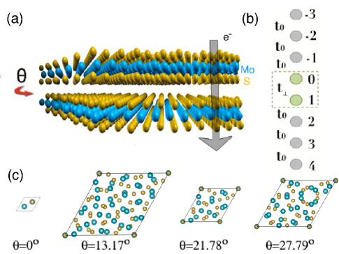
For TMD misoriented bilayers, both experiments and simulations show that the interlayer coupling and the interlayer distance are sensitive to the rotation angle, and that the sensitivity of the coupling is very different for different valleys Liu et al. (2014); Huang et al. (2014); van der Zande et al. (2014); Lui et al. (2015); Yeh et al. (2016). A small rotation angle in hetero-bilayers alters the inter-layer exciton dynamics Yu et al. (2015); Rivera et al. (2016). While the effects of misorientation on the geometry, electronic bandstructure, and vibrational modes of bilayer TMDs have received significant attention, the effect of misorientation on the interlayer resistivity of TMDs has not yet been studied. Recent work considered the effect of misorientation on the in-plane transport AWG . In this work, we theoretically determine the coherent electron and hole interlayer (vertical) conductance of a misoriented MoS2 interface as illustrated in Fig. 1(a).
In MoS2 bilayers, the low-energy electron transport takes place at the valley, and the low-energy hole transport takes place at the valley. This results in an extremely asymmetric response of the electron and hole interlayer conductivity to the interlayer misorientation angle. The coherent interlayer electron transport is exponentially suppressed by the misorientation, and the hole transport is only slightly affected.
Theoretical Methods: The structures considered are a 2H aligned bilayer and misoriented bilayers with commensurate rotation angles. The commensurate unit cells are shown in Fig. 1(c), and they are constructed following the method described in Ref. [Shallcross et al., 2010]. The rotation angles are , , and , and the corresponding unit cell lattice constants are , , where is the lattice constant of 2H aligned bilayer equal to 3.16 ÅPadilha et al. (2014) . Details of the DFT simulation input parameters and output results using the Vienna Ab initio Simulation Package (VASP) Kresse and Hafner (1993); Kresse and Furthmuller (1996); Kresse and Furthmüller (1996); Perdew, Burke, and Ernzerhof (1996); Ernzerhof and Scuseria (1999) are provided in the Appendix.
The purpose of these DFT calculations is to determine the energy splitting of the band edges resulting from the interlayer coupling. The DFT calculations are intentionally performed in the absence of spin-orbit coupling (SOC) to cleanly extract the band splitting from the interlayer coupling Dhall et al. (2016). In the absence of SOC, the energy splitting of each band at wavevector due to the interlayer coupling is . In the basis of the eigenstates of the individual monolayers, the low-energy bilayer Hamiltonian for each band is
| (1) |
where is the low-energy two-dimensional dispersion of band .
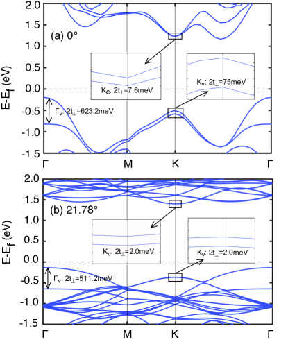
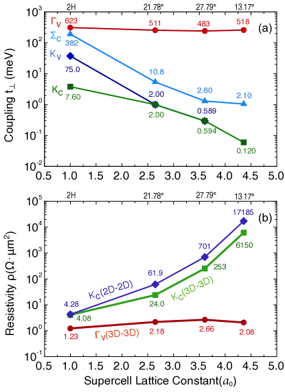
The interlayer couplings are extracted from the energy splittings near the band edge as illustrated in Fig. 2. A semi-log plot of the values versus supercell lattice constant is shown in Fig. 3(a). It is clear from Fig. 3(a) that the interlayer coupling of the holes at are little affected by the misorientation angle. The interlayer couplings of the electron and hole states at and are exponentially suppressed as a function of the supercell lattice constant. This exponential dependence of the band splitting on the supercell lattice constant is also found for the band splitting in rotated bilayer graphene Perebeinos, Tersoff, and Avouris (2012).
Only the conduction valley and the valence valley are considered for calculating the low-energy electron and hole interlayer resistances, since HSE level calculations, which provide more accurate values for energy levels, show that the conduction band valley lies approximately 130 meV below the conduction band valley, and the valence band valley lies 200 meV or more above the valence band valley. Wickramaratne, Zahid, and Lake (2014); Liu et al. (2014); Padilha et al. (2014); Dar . Once we restrict our attention to the conduction valley, which we will denote as , and the valence valley, which we will denote as , spin-orbit splitting has little effect on the inter-layer transport, since the spin splitting of the conduction band at is 1.5 meV and the valence band at is spin degenerate Kormányos et al. (2015). Since we are interested in the room temperature conductance, we ignore the small spin splitting of the conduction band. To a very good approximation, the low-energy bands within the plane (perpendicular to the transport direction) are parabolic and isotropic Kormányos et al. (2015). For the transport calculations, we treat them as parabolic using two masses, and , such that with . The values for the masses from DFT/HSE calculations for the holes at are and for the electrons at are and Peelaers and Van de Walle (2012).
After extracting the interlayer coupling elements from the DFT calculations, we calculate the interlayer conductance of the electron and hole bands using two different methods described below. For low energies near a given valley minimum, the standard 2D-2D tunneling formula is
| (2) |
where is the spectral function of the upper layer, is the spectral function of the lower layer, is the interlayer coupling determined from the band splitting, is the Fermi-Dirac factor, and is the Fermi level of the upper (lower) layer. In the prefactor, is the area, is the spin degeneracy, and is the valley degeneracy. A derivation of this expression from the standard non-equilibrium Green function expression for the current is given in the Appendix. The spectral functions are given by where is the lifetime broadening in each layer and in the second equality, we define . Since the interlayer coupling is a weak function of , we use its value at the band edge. Then, we can perform the sum over the transverse momenta analytically, and Eq. (2) now has the form
| (3) |
For small voltages, the difference in Fermi factors becomes where is the applied voltage, and the integral over gives where is the equilibrium Fermi level. Therefore, the 2D-2D tunneling formula for the interlayer conductivity is
| (4) |
All calculations of the electronic conductivity use a value of meV, and it is estimated from the mobility lifetime using and . For the mobility, we chose 200 cm2/Vs, which is an average of the best measured value for a monolayer of 81 cm2/Vs [Yu et al., 2014] and the theoretical value of 320 cm2/Vs [Jin et al., 2014].
For a given transverse , the transmission resulting from this approach is which has a maximum value of . Since this value must be , it sets an upper limit on the expression’s validity in terms of the magnitude of the coupling with respect to the broadening, meV. For the valley, the unrotated structure does not satisfy this condition, since meV; but for all non-zero rotation angles, this condition is satisfied. For the valley at all rotation angles, it is not.
To have an expression that is also valid for the strongly coupled bands, we create a low-energy, 3D-3D transmission model for each band. Physically, this corresponds to a system of two semi-infinite stacks with one stack rotated with respect to the other resulting in the rotated interface depicted in Fig. 1(a). For each band, at each transverse , this model reduces to that of a one dimensional (1D) tight-binding chain as shown in Fig. 1(b). The hopping parameter is given by of the unrotated bilayer in Fig. 2(a). For this model, the ‘device’ consists of the two misoriented layers numbered 0 and 1 in Fig. 1(b). The ‘device’ Hamiltonian for band is given by Eq. (1). The left and right self-energies due to coupling to the semi-infinite leads are . The Green function is
| (5) |
The transmission is calculated from where . Using the dispersion relation of the leads, , this can be analytically evaluated to obtain where . Going through the same steps as for the 2D-2D tunneling formula, the 3D-3D expression for the conductance is
| (6) |
In all calculations of the interlayer conductance, the Fermi level is taken to be below the conduction band edge when calculating the electron conductance or above the valence band edge when calculating the hole conductance, with T = 300K. The interlayer resistivity is the inverse of the conductivity calculated from Eqs. (4) or (6).
Results and Discussion: Fig. 3(b) shows the interlayer resistivity for electrons at the conduction band edge at and the holes at the valence band edge at . The interlayer resistivity for holes is only calculated from the expression for in Eq. (6), since the 2D-2D tunneling formula is not valid for the holes due to the large value of . The interlayer resistivity for electrons is calculated from both expressions, from Eq. (4) and , and the trends and quantitative values from both expressions match to within a factor of three over 3 orders of magnitude. The agreement is not too surprising since the conductivity resulting from both expressions is proportional to , and the dependence of the electron and hole interlayer conductivity follows the dependence of the interlayer coupling shown in Fig. 3(a).
The physics of the interlayer coupling is determined by the periodic part of the Bloch function (the orbital composition), the phase or envelope , and the interlayer trigonal arrangement of the 3 nearest neighbor Mo atoms in one layer with respect to a Mo atom in the other layer. We will first discuss the valley and then the valley.
First, consider the unrotated 2H bilayer. The very small interlayer coupling of the conduction band is due the symmetry of the conduction band Bloch functions at the points. The conduction band edge at is composed of predominantly Mo orbitals. In a minimal basis, the Bloch state at the conduction band edge of an individual monolayer is where is the position of each Mo atom. The conduction band interlayer coupling is proportional to the the interlayer matrix element where is the matrix element between interlayer, nearest neighbor, Mo orbitals. Since the interlayer matrix element is independent of the azimuthal angle, it is pulled outside of the sum, and the sum of the three phase factors exactly cancel. (For an expanded discussion, see the Supplementary Information of [Jones et al., 2014].)
In contrast, the valence band state at is composed of and orbitals. The interlayer matrix elements between these orbitals change sign as a function of the azimuthal angle preventing the cancellation of the phase factors. Therefore, at the valley of the unrotated structure, even though the conduction band orbitals are out-of-plane and the valence band orbitals are in-plane, the interlayer coupling at is an order of magnitude smaller than the interlayer coupling at , as shown in Fig. 3(a).
Two mechanisms compete to determine the effect of interlayer rotation on the conduction band coupling at . When one layer is rotated with respect to the other, the symmetry is broken, and the exact cancellation of the phases is destroyed. This effect would cause the matrix element to increase. However, now the unit cell size has increased to one of the supercells shown in Fig. 1, and the interlayer matrix elements between all of the orbitals in the supercell and their associated phase factors must be added. At , the phase is changing sign approximately every lattice constant, so that as the wavefunction of the top layer is rotated with respect to that of the bottom layer, and the phases are summed over the large supercell, the matrix element is suppressed by phase cancellation. These two competing effects cause the initial slower decrease in the coupling of the conduction band at compared to the coupling of the valence band at as shown in Fig. 3(a).
The effect of misorientation on the the interlayer resistivity of the electrons at is similar to the effect of misorientation on the interlayer resistivity of electrons and holes in bilayer graphene Bistritzer and MacDonald (2010); Perebeinos, Tersoff, and Avouris (2012); Habib et al. (2013). The electron resistivity increases exponentially with the size of the supercell lattice constant, although the increase in MoS2 is orders of magnitude less than the increase in bilayer graphene (compare Fig. 1d of [Perebeinos, Tersoff, and Avouris, 2012] or Fig. 4 of [Habib et al., 2013] with Fig. 3(b)).
The valence band edge at is composed of 28% S orbitals and 67% Mo orbitalsWickramaratne, Zahid, and Lake (2014). These out-of-plane orbitals, especially the orbitals on the surface S atoms, strongly couple between layers. Furthermore, the interlayer matrix elements are independent of the azimuthal angle, and at , all of the phase factors are 1, so the matrix elements add, and the interlayer coupling is large as shown in Fig. 3(a).
When one layer is rotated with respect to the other, no phase cancellation can occur, since the wavefunctions have no phase. Thus, the holes at are minimally affected by layer rotation. The only effect on the hole coupling is through the slight increase in the interlayer separation causing a slight decrease in the interlayer coupling as shown in Fig. 3(a). Furthermore, the interlayer coupling of the holes monotonically decreases with angle rather than with supercell size, following the monotonic increase of the interlayer distance (see Table S1), which further indicates that different physics govern the effect of misorientation on the electron and hole interlayer coupling.
To gain perspective into what the resistivity values mean for a device application, we consider the target resistivity value of 2.5 m2 for the emitter contact resistance required to achieve THz cutoff frequency in a heterostructure bipolar transistor (HBT) Rodwell, Le, and Brar (2008). The interlayer resistivity of the holes is approximately equal to or below that value for all angles. For all non-zero rotation angles considered, the interlayer resistivity of the electrons is one or more orders of magnitude too high. This suggests design optimization of a heterostructure bipolar transistor (HBT) using stacked TMDs. A pnp HBT will be insensitive to misalignment of the layers. Furthermore, rotating the emitter layer with respect to the base layer in a pnp HBT will increase the emitter injection efficiency by one or more orders of magnitude, since the transmission of electrons injected from the base will be suppressed while the transmission of holes injected from the emitter will be unaffected.
Conclusion: The electron interlayer coupling of the conduction band at is weak (7.6 meV), and it decreases by a factor of 63 as the supercell lattice constant increases by a factor of 4 corresponding to a rotation. The hole coupling is large (632 meV) and remains large decreasing by a factor of 1.3 at a rotation angle of The corresponding electron interlayer resistivity increases from 4 to . The hole resistivity remains near for all rotation angles. Interlayer rotation between an n-type and p-type region will suppress the electron current, which is desirable in the base-emitter junction of a pnp HBT.
Acknowledgement: This work was supported by FAME, one of six centers of STARnet, a Semiconductor Research Corporation program sponsored by MARCO and DARPA. This work used the Extreme Science and Engineering Discovery Environment (XSEDE), which is supported by National Science Foundation grant number ACI-1053575.
*
Appendix A Ab-initio simulation details and derivation of Eq.(2)
Electronic structure calculations of bilayer MoS2 are carried out using density functional theory (DFT) with a projector augmented wave method and the Perdew-Burke-Ernzerhof (PBE) type generalized gradient approximation as implemented in the Vienna Ab initio Simulation Package (VASP) Kresse and Hafner (1993); Kresse and Furthmuller (1996); Kresse and Furthmüller (1996); Perdew, Burke, and Ernzerhof (1996); Ernzerhof and Scuseria (1999). A semi-empirical Grimme-D2 correction to the Kohn-Sham energies is used to model the van der Waals (vdW) interactions Grimme (2006). Spin-orbit coupling is not included, since it has little effect on the interlayer coupling parameter, which is determined by orbital overlap. The plane wave basis energy cutoff is 400 eV. The global break condition for the electronic SC-loop is below eV. The Monkhorst-Pack scheme is used for the integration over the Brillouin zone with a centered k-mesh of for the unrotated thin films. For rotated bilayers, k-mesh are accordingly revised to for , for , for , since they have different Brillouin zones. The k-space integration was carried out with a Gaussian smearing width of 0.02 eV for all calculations. All unit cells were built with 20 separation between replicas in the perpendicular direction to achieve negligible interaction.
The default optimization methods did not efficiently determine the bilayer separation because the van der Waals interaction energies are very small. In order to accurately determine the bilayer separation of each system, several specific layer separations were used to optimize the structures until all or the interatomic forces are below 0.01 eV/ as described in the Supplementary Information of [van der Zande et al., 2014]. The optimized structure with lower total energy was chosen for structure of each rotated angle. The interlayer distances of the relaxed structures are shown in Table S1.
| Angle | d (Å) | (eV) | (eV) | |
|---|---|---|---|---|
| 2H(0) | 1.0 | 6.2568 | 1.3650 | 1.7348 |
| 6.5142 | 1.5279 | 1.7683 | ||
| 6.5287 | 1.5339 | 1.7669 | ||
| 6.5853 | 1.5617 | 1.7698 |
The standard 2D-2D tunneling formula can be obtained following the derivation leading to the current expression of Meir and Wingreen Meir and Wingreen (1992)
| (7) |
For the system shown in Fig. 1(a) of the main text, and are the spectral function and less-than correlation function of the lower layer, and , where is the spectral function of the upper layer. In a tunneling Hamiltonian approach, the two layers are assumed to be weakly coupled, so that each layer can be approximated as equilibrated with its own Fermi level. Then, , and Eq. (7) becomes
| (8) |
References
- Geim and Grigorieva (2013) A. Geim and I. Grigorieva, Nature 499, 419 (2013).
- Kou, Frauenheim, and Chen (2013) L. Kou, T. Frauenheim, and C. Chen, The Journal of Physical Chemistry Letters 4, 1730 (2013).
- Gong et al. (2013) Z. Gong, G.-B. Liu, H. Yu, D. Xiao, X. Cui, X. Xu, and W. Yao, Nature Communications 4 (2013), 10.1038/ncomms3053.
- Wu et al. (2013) S. Wu, J. S. Ross, G.-B. Liu, G. Aivazian, A. Jones, Z. Fei, W. Zhu, D. Xiao, W. Yao, D. Cobden, and X. Xu, Nature Physics 9, 149 (2013).
- Jones et al. (2014) A. M. Jones, H. Yu, J. S. Ross, P. Klement, N. J. Ghimire, J. Yan, D. G. Mandrus, W. Yao, and X. Xu, Nature Physics 10, 130 (2014).
- Lee et al. (2014a) G.-H. Lee, C.-H. Lee, A. M. van der Zande, M. Han, X. Cui, G. Arefe, C. Nuckolls, T. F. Heinz, J. Hone, and P. Kim, APL Mater. 2, 092511 (2014a), 10.1063/1.4894435.
- Lee et al. (2014b) C.-H. Lee, G.-H. Lee, A. M. van der Zande, W. Chen, Y. Li, M. Han, X. Cui, G. Arefe, C. Nuckolls, T. F. Heinz, J. Guo, J. Hone, and P. Kim, Nature Nano 9, 676 (2014b).
- Gong et al. (2014) Y. Gong, J. Lin, X. Wang, G. Shi, S. Lei, Z. Lin, X. Zou, G. Ye, R. Vajtai, B. I. Yakobson, H. Terrones, M. Terrones, B. K. Tay, J. Lou, S. T. Pantelides, Z. Liu, W. Zhou, and P. M. Ajayan, Nature Materials 13, 1135 (2014).
- Zeng et al. (2015) Q. Zeng, H. Wang, W. Fu, Y. Gong, W. Zhou, P. M. Ajayan, J. Lou, and Z. Liu, Small 11, 1868 (2015).
- Zhang et al. (2014) X. Zhang, F. Meng, J. R. Christianson, C. Arroyo-Torres, M. A. Lukowski, D. Liang, J. R. Schmidt, and S. Jin, Nano Letters 14, 3047 (2014).
- van der Zande et al. (2014) A. M. van der Zande, J. Kunstmann, A. Chernikov, D. A. Chenet, Y. You, X. Zhang, P. Y. Huang, T. C. Berkelbach, L. Wang, F. Zhang, M. S. Hybertsen, D. A. Muller, D. R. Reichman, T. F. Heinz, and J. C. Hone, Nano Letters 14, 3869 (2014).
- Liu et al. (2014) K. Liu, L. Zhang, T. Cao, C. Jin, D. Qiu, Q. Zhou, A. Zettl, P. Yang, S. G. Louie, and F. Wang, Nature communications 5, 5966 (2014).
- Huang et al. (2014) S. Huang, X. Ling, L. Liang, J. Kong, H. Terrones, V. Meunier, and M. S. Dresselhaus, Nano letters 14, 5500 (2014).
- Fang et al. (2014) H. Fang, C. Battaglia, C. Carraro, S. Nemsak, B. Ozdol, J. S. Kang, H. A. Bechtel, S. B. Desai, F. Kronast, A. A. Unal, G. Conti, C. Conlon, G. K. Palsson, M. C. Martin, A. M. Minor, C. S. Fadley, E. Yablonovitch, R. Maboudian, and A. Javey, PNAS 111, 6198 (2014).
- Wickramaratne, Zahid, and Lake (2014) D. Wickramaratne, F. Zahid, and R. K. Lake, The Journal of Chemical Physics 140, 124710 (2014).
- Lui et al. (2015) C. H. Lui, Z. Ye, C. Ji, K.-C. Chiu, C.-T. Chou, T. I. Andersen, C. Means-Shively, H. Anderson, J.-M. Wu, T. Kidd, Y.-H. Lee, and R. He, Phys. Rev. B 91, 165403 (2015).
- Rigosi et al. (2015) A. F. Rigosi, H. M. Hill, Y. Li, A. Chernikov, and T. F. Heinz, Nano Letters 15, 5033 (2015).
- Dhall et al. (2015) R. Dhall, M. R. Neupane, D. Wickramaratne, M. Mecklenburg, Z. Li, C. Moore, R. K. Lake, and S. Cronin, Advanced Materials 27, 1573 (2015).
- Dhall et al. (2016) R. Dhall, K. Seyler, Z. Li, D. Wickramaratne, M. R. Neupane, I. Chatzakis, E. Kosmowska, R. K. Lake, X. Xu, and S. B. Cronin, ACS Photonics 3, 310 (2016).
- Gong et al. (2015a) Y. Gong, S. Lei, G. Ye, B. Li, Y. He, K. Keyshar, X. Zhang, Q. Wang, J. Lou, Z. Liu, R. Vajtai, W. Zhou, and P. M. Ajayan, Nano Letters 15, 6135 (2015a).
- Yue et al. (2015) R. Yue, A. T. Barton, H. Zhu, A. Azcatl, L. F. Pena, J. Wang, X. Peng, N. Lu, L. Cheng, R. Addou, S. McDonnell, L. Colombo, J. W. P. Hsu, J. Kim, M. J. Kim, R. M. Wallace, and C. L. Hinkle, ACS Nano 9, 474 (2015).
- He et al. (2016) Y. He, A. Sobhani, S. Lei, Z. Zhang, Y. Gong, Z. Jin, W. Zhou, Y. Yang, Y. Zhang, X. Wang, B. Yakobson, R. Vajtai, N. J. Halas, B. Li, E. Xie, and P. Ajayan, Advanced Materials (2016), 10.1002/adma.201600278.
- Tsoutsou et al. (2016) D. Tsoutsou, K. E. Aretouli, P. Tsipas, J. Marquez-Velasco, E. Xenogiannopoulou, N. Kelaidis, S. A. Giamini, and A. Dimoulas, ACS Applied Materials & Interfaces 8, 1836 (2016).
- Pant et al. (2016) A. Pant, Z. Mutlu, D. Wickramaratne, H. Cai, R. K. Lake, C. Ozkan, and S. Tongay, Nanoscale 8, 3870 (2016).
- Yeh et al. (2016) P.-C. Yeh, W. Jin, N. Zaki, J. Kunstmann, D. A. Chenet, G. Arefe, J. T. Sadowski, J. I. Dadap, P. Sutter, J. C. Hone, and R. M. Osgood, Jr., Nano Letters 16, 953 (2016).
- Gong et al. (2015b) C. Gong, H. Zhang, W. Wang, L. Colombo, R. M. Wallace, and K. Cho, Applied Physics Letters 107, 139904 (2015b), http://dx.doi.org/10.1063/1.4932088.
- Xu et al. (2014) X. Xu, W. Yao, D. Xiao, and T. F. Heinz, Nature Physics 10, 343 (2014).
- Qian et al. (2015) X. Qian, Y. Wang, W. Li, J. Lu, and J. Li, 2D Materials 2, 032003 (2015), 10.1088/2053-1583/2/3/032003.
- Mak and Shan (2016) K. F. Mak and J. Shan, Nature Photonics 10, 216 (2016).
- Yu et al. (2015) H. Yu, Y. Wang, Q. Tong, X. Xu, and W. Yao, Phys. Rev. Lett. 115, 187002 (2015).
- Rivera et al. (2016) P. Rivera, K. L. Seyler, H. Yu, J. R. Schaibley, J. Yan, D. G. Mandrus, W. Yao, and X. Xu, Science 351, 688 (2016).
- (32) Y. Tan, F. Chen, and A. W. Ghosh, ‘First principles study and empirical parametrization of twisted bilayer MoS2 based on band-folding,’ arXiv:1606.01858v1, June 6, 2016.
- Shallcross et al. (2010) S. Shallcross, S. Sharma, E. Kandelaki, and O. Pankratov, Physical Review B 81, 165105 (2010).
- Padilha et al. (2014) J. E. Padilha, H. Peelaers, A. Janotti, and C. G. V. de Walle, Phys. Rev. B 90, 205420 (2014).
- Kresse and Hafner (1993) G. Kresse and J. Hafner, Phys. Rev. B 47, 558 (1993).
- Kresse and Furthmuller (1996) G. Kresse and J. Furthmuller, Comput. Mater. Sci. 6, 15 (1996).
- Kresse and Furthmüller (1996) G. Kresse and J. Furthmüller, Phys. Rev. B 54, 11169 (1996).
- Perdew, Burke, and Ernzerhof (1996) J. P. Perdew, K. Burke, and M. Ernzerhof, Phys. Rev. Lett. 77, 3865 (1996).
- Ernzerhof and Scuseria (1999) M. Ernzerhof and G. Scuseria, J. Chem. Phys. 110, 5029 (1999).
- Perebeinos, Tersoff, and Avouris (2012) V. Perebeinos, J. Tersoff, and P. Avouris, Phys. Rev. Lett. 109, 236604 (2012).
- (41) D. Wickramaratne, ‘Electronic, Vibrational, and Thermoelectric Properties of Two-Dimensional Materials,’ Ph.D. Dissertation, University of California Riverside, 2015. Table A.2.
- Kormányos et al. (2015) A. Kormányos, G. Burkard, M. Gmitra, J. Fabian, V. Zólyomi, N. D. Drummond, and V. Fal’ko, 2D Materials 2, 022001 (2015).
- Peelaers and Van de Walle (2012) H. Peelaers and C. G. Van de Walle, Physical Review B 86, 241401 (2012).
- Yu et al. (2014) Z. Yu, Y. Pan, Y. Shen, Z. Wang, Z.-Y. Ong, T. Xu, R. Xin, L. Pan, B. Wang, L. Sun, et al., Nature communications 5 (2014), 10.1038/ncomms6290.
- Jin et al. (2014) Z. Jin, X. Li, J. T. Mullen, and K. W. Kim, Physical Review B 90, 045422 (2014).
- Bistritzer and MacDonald (2010) R. Bistritzer and A. H. MacDonald, Physical Review B 81, 245412 (2010).
- Habib et al. (2013) K. M. M. Habib, S. S. Sylvia, S. Ge, M. Neupane, and R. K. Lake, Appl. Phys. Lett. 103, 243114 (2013).
- Rodwell, Le, and Brar (2008) M. J. W. Rodwell, M. Le, and B. Brar, Proc. IEEE 96, 271 (2008).
- Grimme (2006) S. Grimme, Journal of Computational Chemistry 27, 1787 (2006).
- Meir and Wingreen (1992) Y. Meir and N. Wingreen, Phys. Rev. Lett. 68, 2512 (1992).