Enhanced Spin-Flip Scattering by Surface Roughness in WS2 and MoS2 Armchair Nanoribbons
Abstract
The band structures of single-layer MoS2 and WS2 present a coupling between spin and valley degrees of freedom that suppresses spin-flip scattering and spin dephasing. Here we show that out-of-plane deformations, such as corrugations or ripples, enhance spin-flip scattering in armchair MoS2 and WS2 nanoribbons. Spin transport in the presence of surface roughness is systematically investigated, employing the non-equilibrium Green’s function method along with the tight-binding approximation. Both transmission and conductance have been calculated as a function of surface roughness. Our results indicate that the spin-flip rate, usually neglected in flat pristine samples, increases significantly with the surface roughness amplitude. These results are important for the design and fabrication of transition metal dichalcogenides based spintronic devices.
pacs:
78.67.Lt, 73.22.-f, 78.20.BhI Introduction
A long spin relaxation length, i.e. the possibility for spin-polarized electrons to travel larger distances without losing encoded information, is a basic requirement for spintronic applications. Graphene was envisioned early on as a promising material for spintronics, owing to the combination of the unique electronic band structure of so-called massless Dirac fermions, weakly sensitive to backscattering and traveling at very high speed over very large distances, even at room temperature. Han et al. (2014); Roche et al. (2015) However the weak spin-orbit coupling (SOC) in graphene makes spin effects very small. The discovery of graphene paved the way for investigating other two-dimensional (2D) materials with properties complementary to those of graphene.Novoselov et al. (2012) Stacking of different families of 2D materials in a controlled fashion can create heterostructures with tailored properties that offers promising avenues to design and fabricate novel devices.Geim and Grigorieva (2013)
Single layers of transition metal dichalcogenides (TMDC) like MoS2 and WS2 are direct band gap semiconductors with strong spin-orbit coupling, which originates from -orbitals of the heavy transition metal atoms. This allows for the control of spin with electric field.Klinovaja and Loss (2013); Ochoa and Roldán (2013); Zibouche et al. (2014); Kormányos et al. (2014); Kośmider and Fernández-Rossier (2013); Georgiou et al. (2013) The band structure of TMDC consists of two inequivalent valleys (K and K’) located at the corners of the hexagonal Brillouin zone.Lebegue and Eriksson (2009) The lack of inversion symmetry alongside the large SOC strength lead to the coupling of spin and valley degrees of freedom,Zeng et al. (2013) allowing for spin and valley control with the potential use of TMDCs in valleytronics and spintronics.Zeng et al. (2012); Sallen et al. (2012); Xiao et al. (2012); Song and Dery (2013) Magneto-transport experiments have estimated an upper limit for the spin-orbit scattering length for -type MoS2 as high as 430 nm.Neal et al. (2013) However mirror symmetry along the -direction is usually broken due to surface ripples, thermal out-of-plane fluctuations, sulfur vacancies, etc., what leads to a Rashba-like spin-orbit contribution which can limit the spin lifetime.Brivio et al. (2011) In particular, static wrinkles have been shown to affect more the spin coherence as compared to out-of-plane phonons.Ochoa et al. (2013)
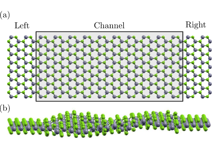
Nanoribbons of TMDCs can be obtained by tailoring a ribbon from an infinitely extended mono-layer,Liu et al. (2013) and can be synthesized by using electrochemical methods,Li et al. (2004) or by unzipping nanotubes.Wang et al. (2010); Nethravathi et al. (2013); Vasu et al. (2015) First-principle calculations indicate that armchair MoS2 and WS2 nanoribbons show semiconducting behaviour, while zigzag nanoribbons are metallic.Li et al. (2008); López-Urías et al. (2015) In this work we study the effect of surface corrugation on spin-transport in armchair nanoribbons of MoS2 and WS2 (Fig. 1). For this we use non-equilibrium Green’s function formalism along with a tight-binding model applied to nanoribbons of TMDCs in the presence of surface roughness. We find a significant increase of spin-flip rate due to static corrugations of the sample. The effects are more important in WS2 than in MoS2, due to the stronger atomic SOC of W atoms. Our results suggest that the use of flat substrates can considerably increase the efficiency of TMDCs for spintronics applications.
The paper is organized as follows. In Sec. II we describe the model and the calculation method, taking into account surface rougness effects. In Sec. III the results are presented and discussed. Finally, in Sec. IV the main conclusions are summarized. In Appendix A we present results obtained considering periodic boundary conditions.
II Model and Method
II.1 Thight Binding Hamiltonian
The crystal structure of TMDCs consist of one triangular lattice of metal atoms (Mo or W in the present case) which is sandwiched between two triangular lattices of chalcogen (S) atoms. Thus the unit-cell contains one transition-metal atom plus two chalcogen atoms. Our calculations will be performed by using a tight-binding model that contains five orbitals of the metal (Mo/W) atoms and three orbitals for each of the two calchogen S atoms in the unit cell.Cappelluti et al. (2013) Therefore the dimension of the Hamiltonian of a single layer (before including spin degrees of freedom) will be , and can be written as:
| (1) |
where are the atomic position indices, and label the atomic orbitals, creates (annihilates) an electron at orbtial of site , refers to on-site crystal fields of orbital and are hopping parameters, where runs over first nearest neighbor sites. The Slater-Koster parameters for MoS2 and WS2 obtained from fits to density functional theory (DFT) calculations are reported in Table 1.Rostami et al. (2015) The ratio of the metal and chalcogen orbital contributions to the valence and conduction bands in our tight-binding model is respectively, in good agreement with DFT calculations.Cappelluti et al. (2013) By performing a unitary transformation that accounts for the symmetric and antisymmetric combinations of S- orbitals of the top and bottom chalcogen atoms, it is possible to simplify the model into two decoupled blocks of dimensions and , being the block the relevant subspace for low energy calculations since it contains the valence and conduction band states. The bases of these blocks are and , respectively,Cappelluti et al. (2013) where and stand for the symmetric and antisymmetric combinations of the top and bottom chalcogen orbitals, , where .
| MoS2 | WS2 | |||||
|---|---|---|---|---|---|---|
| SOC | 0.075 | 0.215 | ||||
| 0.052 | 0.057 | |||||
| Crystal Fields | -1.094 | -0.872 | ||||
| 0.670 | 0.670 | |||||
| -1.511 | -1.511 | |||||
| -3.559 | -3.468 | |||||
| -6.886 | -3.913 | |||||
| -S | 3.689 | 3.603 | ||||
| -1.241 | -0.942 | |||||
| - | -0.895 | -1.216 | ||||
| 0.252 | 0.177 | |||||
| 0.228 | 0.243 | |||||
| S-S | 1.225 | 0.749 | ||||
| -0.467 | 0.236 |
Spin-orbit coupling, however, mixed these blocks through processes that flip the electron spin.Roldán et al. (2014) The SOC contribution is included in our theory trough the term
| (2) |
where is the intra-atomic SOC constant, is the angular momentum operator for atomic orbitals, and is the spin operator. It is useful to express as:
| (3) |
where are the standard ladder operators, with . We can distinguish two different contributions to the SOC Hamiltonian (3), the first term which leads to spin-flip processes, and the spin-conserving term . For flat pristine MoS2 or WS2, spin-flip processes are negligible and full spin polarization as well as long spin relaxation lengths can be achieved.Xu et al. (2014) In this limit one can safely reduce to the block.Roldán et al. (2014) However, as experimentally observed Yeh et al. (2014); Jin et al. (2015) realistic samples do not preserve mirror symmetry along the -direction. This is due to the presence of sulfur vacancies, or to corrugations and ripples in the sample, associated e.g. to the presence of a substrate or due to thermal out-of-plane phonons. In this situation, the and the blocks are coupled. As a consequence, the contribution of and orbitals to the density of states (DOS) of the corrugated ribbon is significantly larger than in the flat situation. Importantly, spin-flip processes become relevant, limiting spin life time.Brivio et al. (2011) Therefore we will use in our calculations the whole Hilbert space of dimension (including spin). We notice that, contrary to previous works that consider the effect of flexural phonons, corrugations or topological defects in the transport properties from minimal models and group theory methods,Song and Dery (2013); Ochoa et al. (2016) here we use a tight-binding model that accurately accounts for the states of the valence and conduction bands in the whole Brillouin zone, to calculate spin-resolved transmission probabilities through a finite corrugated armchair ribbon of MoS2 or WS2.
II.2 Non-equilibrium Green’s function method
The non-equilibrium Green’s function (NEGF) formalism Pourfath (2014) is used to study spin transport in armchair MoS2 and WS2 nanoribbons. The channel and the two contacts are assumed to be of the same material (see Fig. 1). For the calculation of the contact self-energies, the surface Green’s function of the contacts is iteratively solved, employing a highly convergent scheme Sancho et al. (1984, 1985)
| (4) |
where is the energy, is the identity matrix, is the Hamiltonian of the unit cell of the right or left contact in real space representation, is the coupling between two neighboring unit cells in the considered contacts, and is the coupling between the channel and the contacts. Underlined quantities stand for matrices that include both spins. A flat interface is assumed in the contacts, and our calculations include SOC in the channel as well as in the leads. The retarded and advanced Green’s functions of the device region are then given by:
| (5) |
where is a phenomenological broadening (10-5eV), and is the self-energy of the left and right contacts
| (6) |
where is the surface Green’s function of the contacts, given by Eq. (4). The transmission probability is given by
| (7) |
where describes the broadening of the two semi-infinite leads. The spin-resolved transmission probability can be written as:
| (8) |
where and represent parallel spin transmission, and and antiparallel spin-flip transmission.
II.3 Effect of lattice modulation
Different modulations of the lattice have been studied, as bending, sinusoidal ripples and Gaussian corrugation. Here we present results for the Gaussian corrugation although some comments to the other type of disorder will be made. The surface roughness of the substrate is modeled by a Gaussian auto-correlation function:Goodnick et al. (1985); Touski and Pourfath (2013)
| (9) |
where and are the roughness correlation lengths along the and -directions, respectively, and is the root mean square of the variation amplitude. We use in most of our calculations nm. Typical roughness parameters for several common substrate materials are reported in Table 2. As compared to the well studied case of graphene, we notice that the larger bending rigidity of MoS2 causes smoother surface roughness and longer correlation lengths. Surface roughness modulates atomic positions and orbital directions, thus affecting the hopping parameters.
The effect of lattice deformations due to corrugation are considered within our Slater-Koster tight-binding model. If we neglect the corrections to the on-site potentials due to lattice deformation, the effect of strain is thus considered by varying the interatomic bond lengths as a result of the applied strain. The modified hopping terms in the modulated lattice can be written, at the leading order, as
| (10) |
where is the distance between two atoms labelled by and in the unperturbed lattice, the separation in the presence of corrugation, and is the dimensionless bond-resolved local electron-phonon coupling, where and are the considered orbitals in atoms and . The lattice distances are for the in-plane - and - bonds, where is the in-plane inter-atomic distance, and for the - bond. In the absence of any theoretical and experimental estimation for the electron-phonon coupling, we adopt the Wills-Harrison argument Harrison (1999), assuming that depend solely on the total angular momentum of the and orbitals, not on their projections. Namely , where is the absolute value of the angular momentum of the orbital , and is the absolute value of the angular momentum of the orbital . Following this approach we assume that , , and , for the - , for - , and for the - hybridizations, respectively. This approximation has been successfully applied to the study of TMDCs in the presence of non-uniform profiles of strain.Rostami et al. (2015); San-Jose et al. (2016) Importantly, this set of parameters matches the direct-to-indirect bandgap transition in MoS2 under of biaxial strain as obtained from ab-initio calculations.Feng et al. (2012); Wang et al. (2014)
As explained in Sec. II.1, we consider here an intrinsic SOC term in the whole Brillouin zone, including both metal and chalcogen orbitals. This term given by Eq. (3) includes all the spin contributions arising from the crystal potential. The spin-flip terms of the SOC, as discussed before, are negligible in the flat geometries. In the corrugated ribbon, the break of the mirror symmetry produces non-zero matrix elements between the even and odd blocks of the Hamiltonian and therefore spin-flip terms of the become significative. In the rest of the paper we present the results for the spin transport properties of corrugated TMDC ribbons obtained by using the above numerical methods.
III Results and discussion
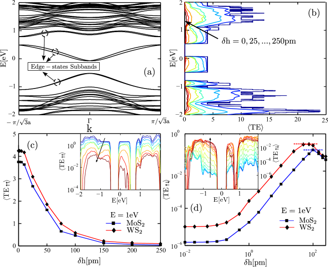
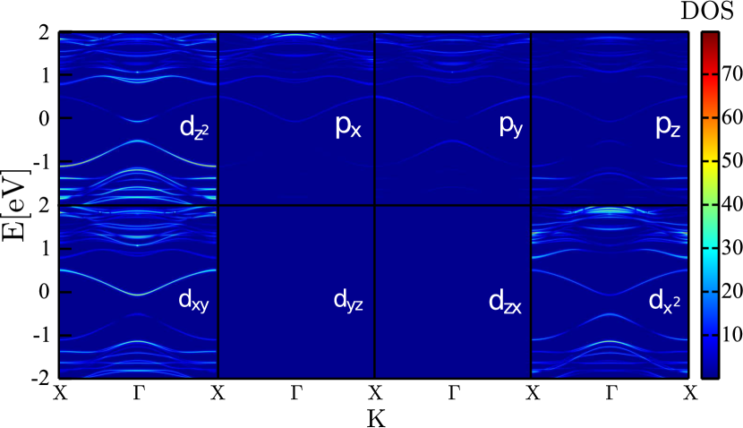
In graphene, it is known that surface roughness mixes with bonds, what enhances spin-orbit interaction.Huertas-Hernando et al. (2006); Chico et al. (2009); López-Sancho and Munoz (2011) In the following we will show which is the effect of sample corrugations on the charge and spin transport properties of TMDCs. The band structure of a MoS2 armchair nanoribbon is shown in Fig. 2(a). In agreement with density functional theory (DFT) calculations,Li et al. (2008); López-Urías et al. (2015) our tight-binding model for the ribbon with this termination shows a semiconducting behaviour, with the appearance of edge states inside the gap, that would be absent if periodic boundary conditions are considered. These edge-state subbands are marked in Fig. 2(a). It is important to notice that the energy bands are spin degenerated and they are split away from the time reversal invariant point of the Brillouin zone due to the effect of SOC.Rostami et al. (2016) The orbital character of each band is shown in Fig. 3. It is interesting to notice that, due to the band folding characteristic of a nanoribbon, the bands at the point present an important contribution from , and for both, valence and conduction states. The ensemble average of the total transmission probability for this system is calculated, by using Eq. (7), for several amplitudes of surface roughness with nm, and the results are shown in Fig. 2(b). In the absence of surface corrugation () the transmission at a given energy is equal to the number of available subbands at that particular energy. For example, around we observe that for (blue line in Fig. 2(b)), which corresponds to the contribution of the two pairs of subbands observed in Fig. 2(a), which are doubly degenerated due to spin. Therefore we observe that the transmission probability for flat nanoribbons is almost unaffected by the spin-orbit interaction.
Realistic samples, however, present surface roughness that modulates the distance and overlap between atomic orbitals. This results in local variations of the hopping parameters and break the surface mirror symmetry. As a consequence, the total transmission decreases with the amplitude of the corrugations. This evolution is shown by the arrow in Fig. 2(b), that shows how the average total transmission decreases with the corrugation amplitude .
In order to investigate the role of surface roughness on spin transport, the spin-resolved transmission have been calculated: and are shown in Fig. 2(c)-(d) as a function of for MoS2 and WS2. It can be observed that (panel (c)) and (panel (d)) present opposite trend with the amplitude of surface corrugation . As expected the spin-conserved transmission (like the the total transmission , panel (b)) decreases with . This behaviour is due to the enhancement of the spin-flip processes in Eq. (7) induced by the variation of the hoppings associated to the sample corrugation. In fact , an indication of spin-flip rate, increases with , as shown in Fig. 2(d). Both quantities, and , are larger for WS2 (diamonds) than for MoS2 (squares). In particular, for WS2 is approximately an order of magnitude larger than that of MoS2 (Fig. 2(d)). This is expected since WS2 has a larger intrinsic spin-orbit coupling than MoS2 (see Table 1), which results in a stronger Rashba-like spin-orbit interaction induced by surface roughness, with the corresponding enhancement of spin-flip processes.
The inset of Fig. 2(d) clearly shows that increases exponentially with roughness amplitude of up to four order of magnitude over a variation of from pm to pm. Interestingly, our calculations also suggest that reaches a maximum for a given value of , and then it starts to decrease. This threshold is about pm for MoS2 and pm for WS2 (see Fig. 2(d)). As explained before two scattering mechanisms affect spin transport: surface corrugation and spin-orbit interaction, which is enhanced with surface roughness. It is also interesting to notice that the spin-flip scattering rate is similar for electron and hole sectors. Since we are dealing with ribbon geometry both, the edge states and the folding of the Brillouin zone, play an important role. In particular, it is very important to notice that the bands (Fig. 2a) are spin degenerate (for both, electron and hole sectors) for the armchair nanoribbons considered here. This is completely different to the case of bulk single layer or zigzag nanoribbons,Rostami et al. (2016) where spin-valley coupling is more robust for valence band states, since valence band edges at K and K’ valleys correspond to opposite spin, and they are well separated in energy from the other subband (the separation is 150 meV for MoS2 and 400 eV for WS2). The armchair termination is a line of dimers with atoms of the two sublattices, therefore the edge states present valley mixing, as it happens in graphene armchair ribbons (see e.g. Refs. Brey and Fertig, 2006; López-Sancho and Munoz, 2011; Yuan et al., 2013). Furthermore, the orbital contribution for the low energy states of both, valence and conduction bands, are rather similar, as it can be seen in Fig. 3. This is due to the band folding that happens for a finite ribbon, with the result that, at the point of the ribbon BZ, there are contributions from ’bulk states’ at and K points. The consequence of this band reconstruction is that, due to the spin degeneracy of the bands and the similar orbital character for electron and hole sectors, the spin-flip scattering probability is of the same order in the two cases.
We have considered other kinds of corrugations like periodic sinusoidal rippling of the sample. We have observed that this kind of corrugation, which can be induced in the laboratory by using elastomeric substrates,Quereda et al. (2016) leads to qualitatively similar effects in the spin-flip transmission (not shown here) but of much weaker magnitude as compared to random Gaussian modulation. We have also checked that bending of the ribbon leads to reduction of as the curvature radius increases. For this case, the polarised transmission is also much smaller than the obtained with the Gaussian corrugation.
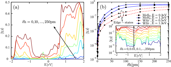
It is interesting to calculate the spin-flip relative transmission (SFRT) , which is a measure of the efficiency of spin control.Michetti et al. (2010) As expected, the ensemble average of as a function of energy (Fig. 4(a)) increases with surface roughness amplitude. We next compare for edge- and bulk-states, as indicated in Fig. 4(b). The amplitude of the edge-state wave functions across the width of the armchair ribbon is originated mainly from -orbitals of the metal (Mo or W) and it is localised at the border atoms, decreasing with the distance to the edge. Our results show that bulk-states are strongly affected by surface roughness, whereas edge-states are more robust against corrugations which results in a lower . This is expected since the spatial localization of edge states protect them partially from surface corrugation effects. The results for transport from purely bulk states are shown in Appendix A, where we show simulations with periodic boundary conditions. At high energies and large , reaches 0.5 that implies a complete loss of spin-information during transmission. This clearly suggest that substrates with rough surfaces, such as the most commonly used SiO2, are not appropriate for spintronic applications based on TMDC materials (see Table 2).
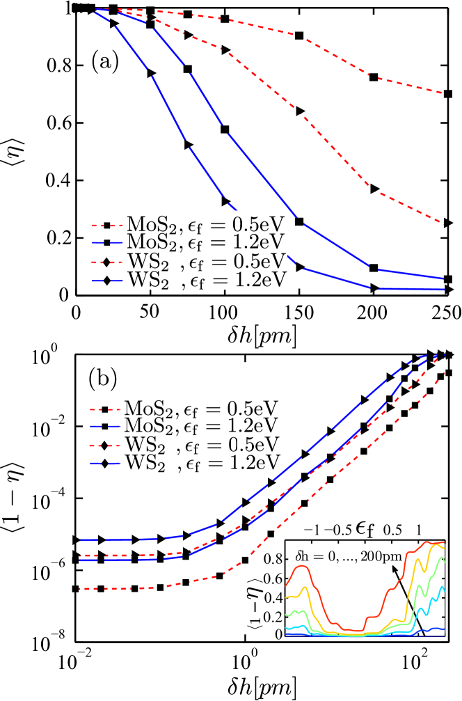
The spin-flip ratio () is another important figure of merit for spintronic devices, defined as
| (11) |
where and , are the spin-conserving and spin-flip conductances respectively.Chico et al. (2015) The conductance in the linear regime is given byRyndyk et al. (2009)
| (12) |
where , is the Fermi-Dirac distribution and is the transmission, Eq. (8). The position of the Fermi level affects the conductance. The results of our calculations are plotted, as a function of roughness amplitudes , in Fig. 5 for eV, coinciding with an edge state band, and for eV, which crosses the bulk bands. The reduction of with suggests again that the spin-flip rate is increased by the surface corrugation. Smaller is observed for higher values of the Fermi energy. This is due to the smaller effect of corrugations on edge states and to the larger density of states at high energies, which cause more spin-flip processes. A similar effect has been observed in graphene.Touski and Pourfath (2013)
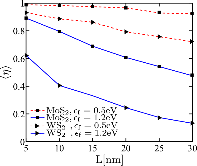
Finally in Fig. 6 we show the dependence of with the channel length, for the the same values of the Fermi energy. We observe that the decay of with the channel length is more pronounced for eV (crossing bulk states) than for eV (crossing edge states). This can be understood again from the fact that spin transport in the second case occurs mainly through the edges, for which we have seen that the effect of corrugations is small. However, when the Fermi level crosses the bulk states, strongly affected by corrugations, decreases faster with the length of the channel.
IV conclusion
In summary, we have performed a systematic theoretical study on spin transport in MoS2 and WS2 armchair nanoribbons in the presence of surface roughness. In the perfectly flat ribbons, the spin-flip terms contribution are negligiblie. Nonetheless, when surface roughness is present, surface mirror symmetry or -axis symmetry is broken generating an additional Rashba-like contribution to the spin-orbit coupling. The strength of this coupling is proportional to the atomic SOC and increases with the corrugation amplitude. Deformation of the surface by ripples, bending or corrugation, modulates the atomic positions thus changing the atomic interactions and orbital hybridisation. The results indicate that sample corrugations significantly enhance the spin-flip rate. For the same surface roughness, the spin-flip rate is larger in WS2 than in MoS2 due to the stronger intrinsic SOC of heavier W atoms. Our results indicate that the spin information can be completely suppressed in TMDCs-based channel with armchair termination supported on rough substrates, such as SiO2. Therefore, the use of flat substrates or the application of techniques to stretch the MoS2 or WS2 samples, avoiding undesirable corrugations, can improve the performance of TMDCs based spintronics devices.
Acknowledgements.
R.R. acknowledges financial support from MINECO (Spain) through grant FIS2014-58445- JIN. M.P.L.S. acknowledges financial support by the Spanish MINECO grant FIS2014-57432-P, the European Union structural funds and the Comunidad de Madrid MAD2D-CM Program (S2013/MIT-3007).Appendix A Simulations with periodic boundary conditions
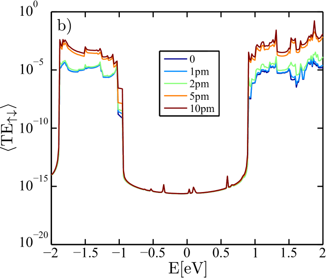
In order to identify the contribution to transport from purely bulk states, in this appendix we present results of calculations done with periodic boundary conditions. The results are shown in Fig. 7. Here the amplitud of the corrugations (10 pm) is much smaller than the used for open boundary conditions (up to 250 pm). This is due to a technical difficulty to obtain the same corrugation in the two edges of the nanoribbon to be connected when periodic boundary conditions are considered. Even for such small corrugations, we observe that due to purely bulk states (there is no edge states present in this calculaton) increases in more than two order of magnitude from a flat nanoribbon to one with corrugations of pm amplitude.
References
- Han et al. (2014) W. Han, R. K. Kawakami, M. Gmitra, and J. Fabian, Nature Nanotech. 9, 794 (2014).
- Roche et al. (2015) S. Roche, J. Åkerman, B. Beschoten, J.-C. Charlier, M. Chshiev, S. P. Dash, B. Dlubak, J. Fabian, A. Fert, M. Guimarães, et al., 2D Mater. 2, 030202 (2015).
- Novoselov et al. (2012) K. S. Novoselov, V. Fal, L. Colombo, P. Gellert, M. Schwab, K. Kim, et al., Nature 490, 192 (2012).
- Geim and Grigorieva (2013) A. Geim and I. Grigorieva, Nature 499, 419 (2013).
- Klinovaja and Loss (2013) J. Klinovaja and D. Loss, Phys. Rev. B 88, 075404 (2013).
- Ochoa and Roldán (2013) H. Ochoa and R. Roldán, Phys. Rev. B 87, 245421 (2013).
- Zibouche et al. (2014) N. Zibouche, P. Philipsen, A. Kuc, and T. Heine, Phys. Rev. B 90, 125440 (2014).
- Kormányos et al. (2014) A. Kormányos, V. Zólyomi, N. D. Drummond, and G. Burkard, Phys. Rev. X 4, 011034 (2014).
- Kośmider and Fernández-Rossier (2013) K. Kośmider and J. Fernández-Rossier, Phys. Rev. B 87, 075451 (2013).
- Georgiou et al. (2013) T. Georgiou, R. Jalil, B. D. Belle, L. Britnell, R. V. Gorbachev, S. V. Morozov, Y.-J. Kim, A. Gholinia, S. J. Haigh, O. Makarovsky, et al., Nat. Nanotechnol. 8, 100 (2013).
- Lebegue and Eriksson (2009) S. Lebegue and O. Eriksson, Phys. Rev. B 79, 115409 (2009).
- Zeng et al. (2013) H. Zeng, G.-B. Liu, J. Dai, Y. Yan, B. Zhu, R. He, L. Xie, S. Xu, X. Chen, W. Yao, et al., Sci. Rep. 3 (2013).
- Zeng et al. (2012) H. Zeng, J. Dai, W. Yao, D. Xiao, and X. Cui, Nat. Nanotechnol. 7, 490 (2012).
- Sallen et al. (2012) G. Sallen, L. Bouet, X. Marie, G. Wang, C. Zhu, W. Han, Y. Lu, P. Tan, T. Amand, B. Liu, et al., Phys. Rev. B 86, 081301 (2012).
- Xiao et al. (2012) D. Xiao, G.-B. Liu, W. Feng, X. Xu, and W. Yao, Phys. Rev. Lett. 108, 196802 (2012).
- Song and Dery (2013) Y. Song and H. Dery, Phys. Rev. Lett. 111, 026601 (2013).
- Neal et al. (2013) A. T. Neal, H. Liu, J. Gu, and P. D. Ye, ACS Nano 7, 7077 (2013).
- Brivio et al. (2011) J. Brivio, D. T. Alexander, and A. Kis, Nano Lett. 11, 5148 (2011).
- Ochoa et al. (2013) H. Ochoa, F. Guinea, and V. Fal’Ko, Phys. Rev. B 88, 195417 (2013).
- Liu et al. (2013) X. Liu, T. Xu, X. Wu, Z. Zhang, J. Yu, H. Qiu, J.-H. Hong, C.-H. Jin, J.-X. Li, X.-R. Wang, et al., Nat. Commun. 4, 1776 (2013).
- Li et al. (2004) Q. Li, J. Newberg, E. Walter, J. Hemminger, and R. Penner, Nano Lett. 4, 277 (2004).
- Wang et al. (2010) Z. Wang, H. Li, Z. Liu, Z. Shi, J. Lu, K. Suenaga, S.-K. Joung, T. Okazaki, Z. Gu, J. Zhou, et al., J. Am. Chem. Soc. 132, 13840 (2010).
- Nethravathi et al. (2013) C. Nethravathi, A. A. Jeffery, M. Rajamathi, N. Kawamoto, R. Tenne, D. Golberg, and Y. Bando, ACS Nano 7, 7311 (2013).
- Vasu et al. (2015) K. Vasu, S. S. Yamijala, A. Zak, K. Gopalakrishnan, S. K. Pati, and C. Rao, Small 11, 3916 (2015).
- Li et al. (2008) Y. Li, Z. Zhou, S. Zhang, and Z. Chen, J. Am. Chem. Soc. 130, 16739 (2008).
- López-Urías et al. (2015) F. López-Urías, A. L. Elías, N. Perea-López, H. R. Gutiérrez, M. Terrones, and H. Terrones, 2D Mater. 2, 015002 (2015).
- Cappelluti et al. (2013) E. Cappelluti, R. Roldán, J. Silva-Guillén, P. Ordejón, and F. Guinea, Phys. Rev. B 88, 075409 (2013).
- Rostami et al. (2015) H. Rostami, R. Roldán, E. Cappelluti, R. Asgari, and F. Guinea, Phys. Rev. B 92, 195402 (2015).
- Roldán et al. (2014) R. Roldán, M. P. Lopez-Sancho, F. Guinea, E. Cappelluti, J. A. Silva-Guillén, and P. Ordejón, 2D Mater. 1, 034003 (2014).
- Xu et al. (2014) X. Xu, W. Yao, D. Xiao, and T. F. Heinz, Nature Physics 10, 343 (2014).
- Yeh et al. (2014) P.-C. Yeh, W. Jin, N. Zaki, D. Zhang, J. T. Sadowski, A. Al-Mahboob, A. M. van der Zande, D. A. Chenet, J. I. Dadap, I. P. Herman, et al., Phys. Rev. B 89, 155408 (2014).
- Jin et al. (2015) W. Jin, P.-C. Yeh, N. Zaki, D. Zhang, J. T. Liou, J. T. Sadowski, A. Barinov, M. Yablonskikh, J. I. Dadap, P. Sutter, et al., Phys. Rev. B 91, 121409 (2015).
- Ochoa et al. (2016) H. Ochoa, R. Zarzuela, and Y. Tserkovnyak, ArXiv e-prints (2016), eprint 1605.07326.
- Pourfath (2014) M. Pourfath, The Non-Equilibrium Green’s Function Method for Nanoscale Device Simulation (Springer, 2014).
- Sancho et al. (1984) M. P. L. Sancho, J. M. L. Sancho, and J. Rubio, J. Phys. F: Met. Phys. 14, 1205 (1984).
- Sancho et al. (1985) M. P. L. Sancho, J. M. L. Sancho, and J. Rubio, J. Phys. F: Met. Phys. 15, 851 (1985).
- Goodnick et al. (1985) S. Goodnick, D. Ferry, C. Wilmsen, Z. Liliental, D. Fathy, and O. Krivanek, Phys. Rev. B 32, 8171 (1985).
- Touski and Pourfath (2013) S. B. Touski and M. Pourfath, Appl. Phys. Lett. 103, 143506 (2013).
- Harrison (1999) W. A. Harrison, Elementary electronic structure (World Scientific, 1999).
- San-Jose et al. (2016) P. San-Jose, V. Parente, F. Guinea, R. Roldán, and E. Prada, Phys. Rev. X 6, 031046 (2016).
- Feng et al. (2012) J. Feng, X. Qian, C.-W. Huang, and J. Li, Nat. Photon. 6, 866 (2012).
- Wang et al. (2014) L. Wang, A. Kutana, and B. I. Yakobson, Ann. Phys. 526, L7 (2014).
- Yamamoto et al. (2015) M. Yamamoto, S. Dutta, S. Aikawa, S. Nakaharai, K. Wakabayashi, M. S. Fuhrer, K. Ueno, and K. Tsukagoshi, Nano Lett. 15, 2067 (2015).
- Sercombe et al. (2013) D. Sercombe, S. Schwarz, O. Del Pozo-Zamudio, F. Liu, B. Robinson, E. Chekhovich, I. Tartakovskii, O. Kolosov, and A. Tartakovskii, Sci. Rep. 3 (2013).
- Quereda et al. (2014) J. Quereda, A. Castellanos-Gomez, N. Agraït, and G. Rubio-Bollinger, Appl. Phys. Lett. 105, 053111 (2014).
- Azcatl et al. (2014) A. Azcatl, S. McDonnell, K. Santosh, X. Peng, H. Dong, X. Qin, R. Addou, G. I. Mordi, N. Lu, J. Kim, et al., Appl. Phys. Lett. 104, 111601 (2014).
- Yu et al. (2013) Y. Yu, C. Li, Y. Liu, L. Su, Y. Zhang, and L. Cao, Sci. Rep. 3 (2013).
- Ji et al. (2013) Q. Ji, Y. Zhang, T. Gao, Y. Zhang, D. Ma, M. Liu, Y. Chen, X. Qiao, P.-H. Tan, M. Kan, et al., Nano Lett. 13, 3870 (2013).
- Huertas-Hernando et al. (2006) D. Huertas-Hernando, F. Guinea, and A. Brataas, Phys. Rev. B 74, 155426 (2006).
- Chico et al. (2009) L. Chico, M. P. López-Sancho, and M. C. Muñoz, Phys. Rev. B 79, 235423 (2009).
- López-Sancho and Munoz (2011) M. López-Sancho and M. Munoz, Phys. Rev. B 83, 075406 (2011).
- Rostami et al. (2016) H. Rostami, R. Asgari, and F. Guinea, J. Phys.: Condens. Matter 28, 495001 (2016).
- Brey and Fertig (2006) L. Brey and H. A. Fertig, Phys. Rev. B 73, 235411 (2006).
- Yuan et al. (2013) S. Yuan, R. Roldán, A.-P. Jauho, and M. I. Katsnelson, Phys. Rev. B 87, 085430 (2013).
- Quereda et al. (2016) J. Quereda, P. San-Jose, V. Parente, L. Vaquero-Garzon, A. J. Molina-Mendoza, N. Agraït, G. Rubio-Bollinger, F. Guinea, R. Roldán, and A. Castellanos-Gomez, Nano Lett. 16, 2931 (2016).
- Michetti et al. (2010) P. Michetti, P. Recher, and G. Iannaccone, Nano Lett. 10, 4463 (2010).
- Chico et al. (2015) L. Chico, A. Latgé, and L. Brey, Phys. Chem. Chem. Phys. 17, 16469 (2015).
- Ryndyk et al. (2009) D. Ryndyk, R. Gutiérrez, B. Song, and G. Cuniberti, in Energy Transfer Dynamics in Biomaterial Systems (Springer, 2009), pp. 213–335.