Effect of the edge states on the conductance and thermopower in Zigzag Phosphorene Nanoribbons
Abstract
We numerically study the effect of the edge states on the conductance and thermopower in zigzag phosphorene nanoribbons (ZPNRs) based on the tight-binding model and the scattering-matrix method. It is interesting to find that the band dispersion, conductance, and thermopower can be modulated by applying a bias voltage and boundary potentials to the two layers of the ZPNRs. Under the certain bias voltage, the two-fold degenerate quasi-flat edge bands split perfectly. The conductance can be switched off, and the thermopower around zero energy increases. In addition, when only the boundary potential of the top layer or bottom layer is adjusted, only one edge band bends and merges into the bulk band. The first conductance plateau is strongly decreased to around zero energy. Particularly, when the two boundary potentials are adjusted, all the edge bands bend and fully merge into the bulk band, and the bulk energy gap is maximized. More interestingly, a pronounced conductance plateau with is found around zero energy, which is attributable to the opening of the bulk energy gap between the valence and conduction bands. Meanwhile, the thermopower can be enhanced more than twice, compared to that of the perfect ZPNRs. The large magnitude of thermopower is ascribed to the appearance of the bulk energy gap around zero energy. Our results show that the modulated ZPNRs are more reliable in thermoelectric application.
I Introduction
Two-dimensional (2D) layered crystal materials have attracted considerable attention due to their unique electric properties Liao2010 ; Schwierz2010 ; Wu2011 ; Mak2010 ; Radisavljevic2011 ; Yoon2011 . Graphene is known to possess excellent electronic properties such as high carrier mobility and tunable carrier type and density, but its zero band gap limits its performance Liao2010 ; Schwierz2010 ; Wu2011 . Transition-metal dichalcogenide MoS2 is found to be a direct band gap semiconductor, but the carrier mobility can only reach 200 Mak2010 ; Radisavljevic2011 ; Yoon2011 . Very recently, another new semiconducting material, called black phosphorus, has attracted much attention because of its great transport properties and potential applications Reich2014 ; Li2015 ; Liu2014 ; Qiao2014 ; Xia2014 ; Koenig2014 ; Gomez2014 ; Li2014 . Black phosphorus is a layered material, in which individual atomic layers are stacked together by van der Waals interactions, and the phosphorene is another 2D stable elemental material that can be mechanically exfoliated from bulk black phosphorus Li2014 ; Liu2014 . Within a phosphorene sheet, every phosphorous atom is covalently bonded with three neighboring atoms forming a highly corrugated honeycomb-like structure with low symmetry and high anisotropy. Unlike the zero-gap semimetal graphene, phosphorene exhibits a direct band gap that can be modified from 1.51 of a monolayer to 0.59 of five layers Qiao2014 . Experiments Li2015 have shown that black phosphorus exhibits an integer Quantum Hall Effect. Field effect transistors based on few layers of phosphorene have been reported to show high performance at room temperatures with an on/off ratio up to and a much larger mobility than MoS2, up to 1000 Li2014 ; Liu2014 ; Gomez2014 ; Xia2014 , making it a promising candidate material for electronic device applications. On the other hand, experimental measurements Flores2015 of the thermoelectric power of bulk black phosphorus demonstrated that its Seebeck coefficient at room temperatures is 335, and the thermopower increases with temperature, suggesting that black phosphorus also has great potential in thermoelectric applications Qin2014 ; Lv2014 ; Fei2014 ; Peng2013 .
One-dimensional (1D) nanoribbons etched or patterned from above 2D materials can offer even more tunability in electronic properties because of the unique quantum confinement and edge effects. The electronic properties of the phosphorene nanoribbons (PNRs), especially the zigzag phosphorene nanoribbons (ZPNRs), have been studied Tran2014 ; Ezawa2014 ; Sisakht2015 ; Guo2014 ; Han2014 . It was found that the pristine ZPNRs are metals regardless of the ribbon widths, while the pristine Armchair PNRs (APNRs) are semiconductors with indirect band gaps Guo2014 . The band gap and the transport properties of the PNRs can be dramatically modified by tensile strain and external in-plane electric-field Guo2014 ; Han2014 ; Ezawa2014 ; Sisakht2015 . The possible structural reconstruction in the edge of the PNRs has also been investigated Carvalho2014 . More recently, theoretical studies find intriguing properties in skewed-ZPNRs and skewed-APNRs. The skewed-APNRs is particularly interesting since it has two quasi-flat bands in the middle of the band gap for the band structure. They share the same topological origin as those in the normal ZPNRs Peeter2016 . On the other hand, the first-principle calculations Zhang2014 showed that in the ZPNRs, the Seebeck coefficient around the Fermi level exhibits very small value, but can be greatly enhanced by hydrogen passivation at the edge. The resulting giant Seebeck coefficient is very beneficial for their thermoelectric applications. In the experiment, Chang-Ran Wang Wang2011 demonstrate that the thermopower can be enhanced greatly at a low temperature by using a dual-gated bilayer graphene device, which has been predicted theoretically and originates from the opening of a band gap hao2010 . Up to now, there are no experimental studies on tuning the thermopower of the ZPNRs. Owing to the unique structure and edge effect, the ZPNRs are expected to exhibit rich novel electric and thermoelectric transport properties under external electric field. However, theoretical studies of the electric and thermoelectric transport of the ZPNRs are limited, compared with those of other 2D materials Zhu2010 ; Ma2011 ; Fan2014 ; Peng2016 . In particular, a detailed investigation about the effect of the edge states on the conductance and thermopower of the ZPNRs, in the presence of an applied bias voltage, has not been carried out so far, which is highly desired. Such theoretical study will provide useful theoretical predicting and guidance to the experimental research of the electric and thermoelectric transport in these systems.
In this paper, we perform numerical study of the effect of edge states on the conductance and thermopower in the ZPNRs based on the tight-binding model and scattering-matrix method. We find that the edge band dispersion, conductance, and thermopower can be modulated by applying an electrostatic bias voltage between the top and bottom layers and boundary potentials to the layers of the ZPNRs. Under certain bias voltage, the two-fold degenerate quasi-flat edge band splits completely. The first conductance plateau around zero energy becomes , compared to that of the perfect ZPNRs. The thermopower around zero energy can be enhanced by increasing the bias voltage. When only the boundary potential of the top layer or bottom layer is adjusted, only one edge state bends and merges into the bulk band. Around zero energy, the first conductance plateau is strongly reduced to . Particularly, when the two boundary potentials are adjusted, all the edges states bend and fully merge into the bulk band and the bulk energy gap is maximized. More interestingly, a pronounced plateau with emerges around zero energy, which can only be understood as due to the opening of the bulk energy gap between the valence and conduction bands. Meanwhile, the thermopower is enhanced more than twice, compared to that of the perfect ZPNRs. We attribute the large magnitude of thermopower to the appearance of the bulk energy gap around zero energy.
This paper is organized as follows. In Sec. II, the model Hamiltonian for zigzag phosphorene nanoribbons is introduced. In Sec. III, numerical results from the exact calculations based on the Landauer-Büttiker are presented. The final section contains a summary.
II Model and Methods
The unit cell of phosphorene contains four phosphorus atoms, where two phosphorus atoms sit on the top layer and the other two sit on the bottom layer. The tight-binding model Hamiltonian of phosphorene Rudenko2014 with a bias voltage can be described by
| (1) |
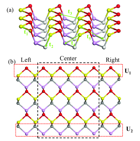
Here, the summation of runs over all neighboring lattice sites with as the hopping integrals, and and are the creation and annihilation operators of electrons on site . The hopping integrals between a site and its neighbours are illustrated in Fig.1(a). The hopping integral corresponds to the connection in each zigzag chain in the upper or lower layer, and stands for the connection between a pair of zigzag chains in the upper and lower layers. is between the nearest-neighbour sites of a pair of zigzag chains in the upper or lower layer, and is between the next nearest-neighbour sites of a pair of zigzag chains in the upper and lower layers. is the hopping between two atoms on upper and lower zigzag chains that are farthest from each other. The values of these hopping integrals are , , , , and Rudenko2014 . The system has negative hopping integral along the zigzag chains, and positive hopping integral connecting the zigzag chains. In the presence of a uniform perpendicular electric field, the top and bottom layers gain different electrostatic potentials and , which are taken to be antisymmetric, namely, Ma2011 ; Ma2009 . If we choose a relatively small potential =0.1, the realistic magnitude of the electric field is about 0.29 . This is experimentally feasible zhang2009 .
We consider a zigzag PNR with two terminals, as shown in Fig.1(b). While a system with is shown in the schematic view, much larger sizes are adopted in the following actual numerical calculations. The linear conductance is calculated by using the Landauer-Büttiker formula Landauer1970 ; Datta1995 ; Lv2012
| (2) |
where is the Fermi distribution function. is the transmission coefficient, which can be calculated by using the Kwant package Groth2014 , with the superscripts and indicating the left and right leads, respectively. The thermopower can be calculated by using the formula Lv2012
| (3) |
III Results and Discussion
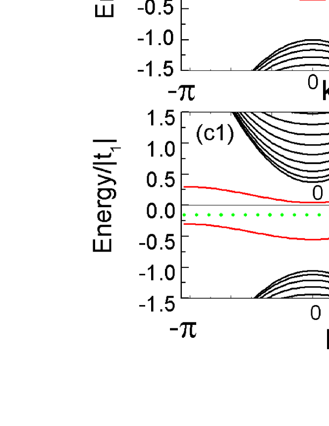
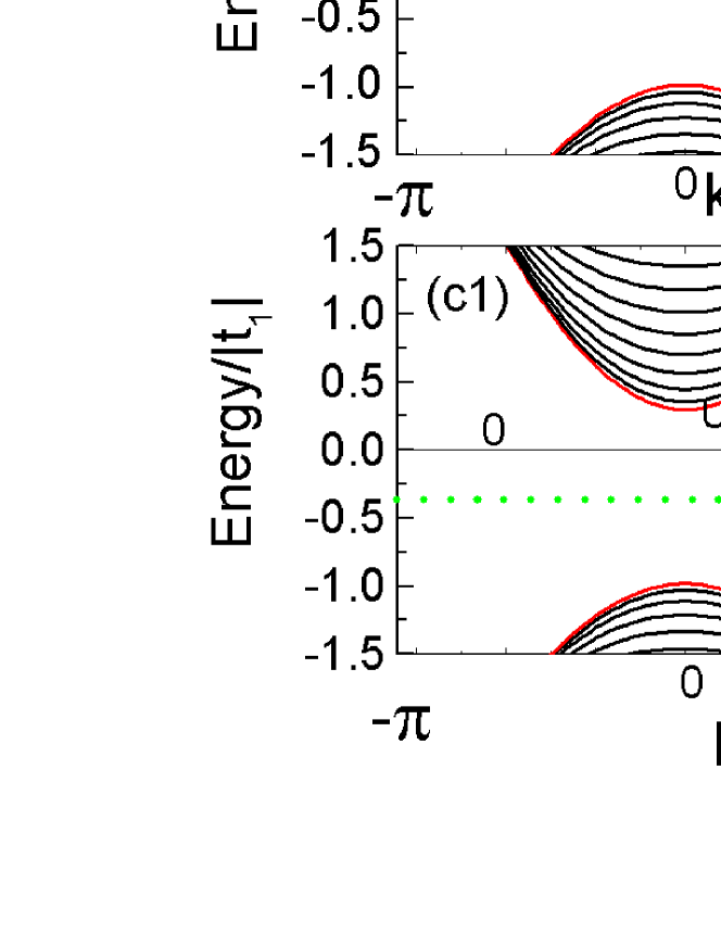
The band structure and conductance of the ZPNRs at zero temperature obtained by numerical diagonalization of the tight-binding Hamiltonian are plotted in Fig.2. The results of the perfect ZPNRs without applied bias voltage are shown in Figs.2(a). As can be seen from Fig.2(a1), the upper and lower quasi-flat edge bands around the Fermi level are detached from the bulk bands, and are two-fold degenerate. The wave functions of the quasi-flat bands are always localized near the sample edges. The conductance shown in Fig.2(a2) displays a clear stepwise structure. When the Fermi energy crosses the discrete transverse channels, the quantized transmission coefficient jumps from one step to another. The quantized conductance plateaus follow the sequence with as positive integers. The first conductance plateau at the Fermi energy is . The conductance plateaus in the conduction band or valence band are not equidistant in energy. The widths of conductance plateaus are determined by the energy scale between the successive modes in the energy spectrum, which depends on the ribbon width and energy interval. Our calculated results are in good agreement with those obtained by Ezawa Ezawa2014 ; Sisakht2015 . However, when a bias voltage or a potential difference is applied to the top and bottom phosphorene sheets, the band structure and conductance show remarkable different features. In Figs. 2(b)-(c), we show the calculated band structure and conductance for the ZPNRs in the presence of an applied bias voltage. As seen from Figs.2(b1) and (b2), the potential difference between the top and bottom phosphorene sheets lifts the degeneracy of the two edge modes, shifting one edge mode upward and the other downward without changing their shapes. The original first conductance plateau still exists, but its width decreases, and a new conductance plateau of appears around the Fermi energy. When the bias voltage increases to , the upper and lower quasi-flat edge bands split completely, and the minimal conductance becomes around the Fermi energy, as shown in Figs.2(c1) and (c2). This feature suggests that the biased ZPNRs can serve as field-effect transistors, whose conductance can be switched on and off by a potential difference between the top and bottom phosphorene sheets.
We further calculate the thermopower using Eq. (3), which can be directly determined in experiments by measuring the responsive electric fields. In the right side of the Fig.2, we show the calculated thermopower for some different bias voltages. According to the definition of the thermopower, is determined by the electron-transmission-weighted average value of the heat energy -. In Fig.2(a3), for metallic ZPNRs without the bias voltage, only the carriers within several around the Fermi energy are important for transport. Thus the average heat energy is in the order of , which results in a much smaller thermopower. However, when a bias voltage or a potential difference is applied to the top and bottom phosphorene sheets, the peak value of around zero energy increases. With the increase of , the peak height of increases to () at , as shown in Fig.2(c3). Around zero energy point, the sign of thermopower changes abruptly. This is because near zero energy point the transmission coefficient is zero and the carriers cannot be transmitted. The large magnitude of the thermopower is mainly due to the split of the two-fold degenerate quasi-flat edge bands and the existence of the energy gap in biased ZPNRs, so that the electrons at the conduction subband edge, which are responsible for electron conduction at the maximum thermopower, have a much larger - compared to the case of without applied bias voltage. This is similar to the corresponding behavior in semiconducting armchair graphene nanoribbons ouyang2009 ; xing2009 ; hao2010 . The maximum magnetitude of thermopower, which is reached with Fermi energy near the middle of the band gap. The greatly enhanced thermopower is very beneficial for the thermoelectric applications of the ZPNRs.
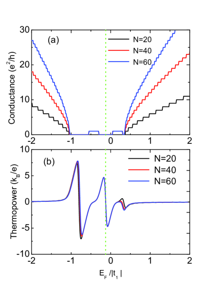
Next, we study the effect of the ribbon width on the conductance and thermopower of the ZPNRs. In Fig.3, we show the conductance at zero temperature and thermopower for three different ribbon widths at fixed bias voltage . As we see from Fig.3(a), with the increase of ribbon width, the characteristics of the conductance are qualitatively similar. Around zero energy, the conductance plateaus remain unchanged, which are independent of the width of the ribbon. Moreover, the widths of the other conductance plateaus away from zero energy become smaller for and with increasing the ribbon widths. As seen from Fig.3(b), the peak value of around zero energy is nearly unchanged with the increase of the ribbon width. Therefore, we can conclude that the characteristic features of the conductance and thermopower around zero energy are insensitive to the ribbon width.
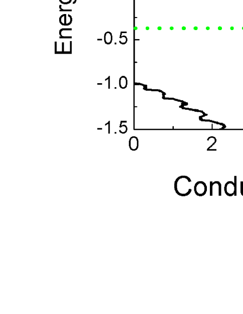
We also study the disorder effect on the conductance and thermopower in ZPNRs without applied bias voltage. In our numerical calculation, we consider the on-site Anderson disorder, and the on-site potential energy is assumed to distribute uniformly in the region of , with disorder strength . Here, the random on-site potential is considered only in the central scattering region. In Fig.4, the conductance and thermopower are shown as a function of for three different disorder strengths. For comparison, the calculated conductance and thermopower for a clean ZPNRs are plotted in Fig.4(a). As the increase of the disorder, it is found that the conductance and thermopower are strongly affected. As can be seen from Fig.4(b), the original first conductance plateaus at the Fermi energy begins to collapse even in the small disorder. In Fig.4(c), at a relatively strong-disorder strength , the first conductance plateaus with disappears completely, and a new conductance plateau with is found, which can only be understand as due to the opening of energy gap between the valence and conduction bands. So, the peak value of around zero energy is enhanced to (). Therefore, we can conclude that the characteristic features of the conductance and thermopower at Fermi energy are strongly affected by the disorder.
In the following, we focus on how the band structure, conductance and thermopower are affected by the boundary potentials for the ZPNRs subject to a weak bias voltage. The on-site energy is in the top layer and in the bottom layer. The boundary potentials and can also be adjusted by potentials applied on the boundaries in both layers Yao2009 , as shown in Fig.1(b). When the boundary potentials and are adjusted in proper order, the band structure, conductance and thermopower show significant properties. In Fig.5, we first show the results of the band structure and conductance at zero temperature. As seen from Fig.5(a1), when only one boundary potential is applied to the top layer, it is found that only one edge band bends and fully merges into the bulk valence band. Around zero energy, the first conductance plateau is strongly reduced to , as shown in Fig.5(a2). Compared with that of the perfect ZPNRs, the metallic nature decreases. When only one boundary potential is applied to the bottom layer, it is found that only one edge band (the lower edge state) bends and merges into the bulk conduction band, as shown in Fig.5(b1). The behavior of the conductance is the same as in Fig.5(a2).
However, when the two boundary potentials and are adjusted to , both edge bands bend and fully merge into the bulk band, and the bulk energy gap is maximized, as shown in Fig.5(c1). More interestingly, the quantized conductance plateaus follow sequence with , as shown in Fig.5(c2). Around zero energy, a pronounced plateau with is found, which can only be understood as due to the opening of the bulk energy gap between the valence and conduction bands Ma2011 . Compared with that of the perfect ZPNRs, the conductance is strongly suppressed, and the metallic characteristic disappears.
In the right side of Fig.5, we show the calculated thermopower for different boundary potentials. As we can see, when only one boundary potential of the top layer is adjusted to , the peak value of near zero energy is about (), as shown in Fig.5(c1). When the other boundary potential of the bottom layer is adjusted to , the behavior of is the same as the case for . In Fig.5(c3), when the two boundary potentials and are adjusted to , it is interesting to notice that has a much larger peak value around zero energy. The peak value of is about (), increasing more than twice, compared to the result of the perfect ZPNRs. We attribute the large magnitude of to the opening of the bulk energy gap near zero energy Ma2011 . Such an enhanced thermopower of the ZPNRs is very beneficial for their thermoelectric applications.
IV Summary
In summary, we have numerically investigated the effect of edge states on the conductance and thermopower in the ZPNRs based on the tight-binding model and scattering-matrix method. We find that the edge band structure, conductance, and thermopower can be modulated by adjusting the bias voltage and boundary potentials. Under the certain bias voltage , the two-fold degenerate quasi-flat bands split completely, one edge mode shifts upward and the other shifts downward without changing their shapes. The first conductance plateau around zero energy decreases to , compared to that of the perfect ZPNRs. Meanwhile, the thermopower around zero energy increases.
On the other hand, when the boundary potentials are adjusted, the band structure, conductance and thermopower show remarkable new features. When only one boundary potential of the top layer or the bottom layer is applied, it is interesting to find that only one edge band bends and merges into the bulk band. Around zero energy, the first conductance plateau is strongly reduced to . However, when both boundary potentials and are applied, both edge bands bend and fully merge into the bulk band, and the bulk energy gap is maximized. More interestingly, a pronounced plateau with is found around zero energy, which can only be understood as due to the opening of the bulk energy gap between the valence and conduction bands. The conductance is strongly suppressed, and the metallic characteristic disappears. Meanwhile, the thermopower is enhanced more than twice, compared to the result of the perfect ZPNRs. We attribute the large magnitude of to the opening of the bulk energy gap around zero energy.
Acknowledgements.
This work was supported by the National Natural Science Foundation of China under grant numbers 11104146, 11574155, 11681240385 (R.M.), 11225420 (L.S.), 11174125, 91021003 (D.Y.X) and a project funded by the PAPD of Jiangsu Higher Education Institutions. This work was also supported by the State Key Program for Basic Researches of China under grant numbers 2015CB921202, 2014CB921103 (L.S.) and the Postdoctoral Science Foundation of China under grant numbers 2014M551546, 2015T80532(R.M.).References
- (1) L. Liao, Y. C. Lin, M. Bao, R. Cheng, J. Bai, Y. Liu, Y. Qu, K. L. Wang, Y. Huang, and X. Duan, Nature 467, 305 (2010).
- (2) F. Schwierz, Nat. Nanotechnol. 5, 487 (2010).
- (3) Y. Wu, Y. M. Lin, A. A. Bol, K. A. Jenkins, F. Xia, D. B. Farmer, Y. Zhu, and P. Avouris, Nature 472, 74 (2011).
- (4) K. F. Mak, C. Lee, J. Hone, J. Shan, and T. F. Heinz, Phys. Rev. Lett. 105, 136805 (2010).
- (5) B. Radisavljevic, A. Radenovic, J. Brivio, V. Giacometti, and A. Kis, Nat. Nanotechnol. 6, 147 (2011).
- (6) Y. Yoon, K. Ganapathi, and S. Salahuddin, Nano Letters 11, 3768 (2011).
- (7) E. S. Reich, Nature 506, 19 (2014).
- (8) Likai Li, Fangyuan Yang, Guo Jun Ye, Zuocheng Zhang, Zengwei Zhu, Wen-Kai Lou, Liang Li, Kenji Watanabe, Takashi Taniguchi, Kai Chang, Yayu Wang, Xian Hui Chen and Yuanbo Zhang, cond-mat/arXiv:1504.07155.
- (9) L. Li, Y. Yu, G. J. Ye, Q. Ge, X. Ou, H. Wu, D. Feng, X. H. Chen, and Y. Zhang, Nature Nanotech. 9, 372 (2014).
- (10) H. Liu, A. T. Neal, Z. Zhu, D. Tománek and P. D. Ye, ACS Nano 8, 4033 (2014).
- (11) F. Xia, H. Wang, and Y. Jia, Nat. Commun. 5, 4458 (2014).
- (12) A. Castellanos-Gomez, L. Vicarelli, E. Prada, J. O. Island, K. L. Narasimha-Acharya, S. I. Blanter, D. J. Groenendijk, M. Buscema, G. A. Steele, J. V. Alvarez, H. W. Zandbergen, J. J. Palacios, and H. S. J. van der Zant, 2D Mater. 1, 025001 (2014).
- (13) S. P. Koenig, R. A. Doganov, H. Schmidt, A. H. Castro Neto, and B. zyilmaz, Appl. Phys. Lett. 104, 103106 (2014).
- (14) J. Qiao, X. Kong, Z.X. Hu, F. Yang and W. Ji, Nat. Commun. 5, 4475 (2014).
- (15) E. Flores, J. R. Ares, A. Castellanos-Gomez, M. Barawi, I. J. Ferrer, and C. Sánchez Appl. Phys. Lett. 106, 022102 (2015).
- (16) G. Qin, Q.B. Yan, Z. Qin, S.Y. Yue, H.J. Cui, Q.R. Zheng, and G. Su, Scientific Reports 4, 6946 (2014).
- (17) H. Y. Lv, W. J. Lu, D. F. Shao, and Y. P. Sun, Phys. Rev. B 90, 085433 (2014).
- (18) R. Fei, A. Faghaninia, R. Soklaski, J. A. Yan, C. Lo, and L. Yang, Nano Lett, 14, 6393 (2014).
- (19) Q. Peng, and S. De, Physical Chemistry Chemical Physics, 15, 19427 (2013).
- (20) V. Tran and L. Yang, Phys. Rev. B 89, 245407 (2014).
- (21) M. Ezawa, New J. Phys., 16, 115004(2014).
- (22) E.T. Sisakht, M.H. Zare, and F. Fazileh, Phys. Rev. B 91, 085409 (2015).
- (23) H. Guo, N. Lu, J. Dai, X. Wu, and X. C. Zeng, J. Phys. Chem. C 118, 14051 (2014).
- (24) X. Y. Han, H. M. Stewart, S. A. Shevlin, C.R.A. Catlow and Z. X. Guo, Nano Lett. 14, 4607 (2014).
- (25) A. Carvalho, A. S. Rodin and A. H. Castro Neto, Europhysics Letters, 108, 47005 (2014).
- (26) Marko M. Grujic, Motohiko Ezawa, Milan Z. Tadic, and Francois M. Peeters, Phys. Rev. B 93, 245413 (2016).
- (27) J. Zhang, H. J. Liu, L. Cheng, J. Wei, J. H. Liang, D. D. Fan, J. Shi, X. F. Tang and Q. J. Zhang, Scientific Reports, 4, 6452 (2014).
- (28) Chang-Ran Wang, Wen-Sen Lu, Lei Hao, Wei-Li Lee, Ting-Kuo Lee, Feng Lin, I-Chun Cheng, and Jian-Zhang Chen, Phys. Rev. Lett. 107, 186602 (2011).
- (29) Lei Hao and T. K. Lee, Phys. Rev. B 81, 165445 (2010).
- (30) L. Zhu, R. Ma, L. Sheng, M. Liu, and D. N. Sheng, Phys. Rev. Lett. 104, 076804 (2010).
- (31) R. Ma, L. Zhu, L. Sheng, M. Liu, and D. N. Sheng, Phys. Rev. B 84, 075420 (2011); R. Ma, L. Sheng, M. Liu, and D. N. Sheng, ibid. 86, 115414 (2012).
- (32) D. D. Fan, H. J. Liu, L. Cheng, P. H. Jiang, J. Shi, X. F. Tang, Appl. Phys. Lett. 105, 133113 (2014).
- (33) Z. Zhang, Y. Xie, Q. Peng, Y. Chen, Scientific Reports, 6, 21639 (2016).
- (34) A. N. Rudenko and M. I. Katsnelson, Phys. Rev. B 89, 201408 (2014).
- (35) R. Ma, L. Zhu, L. Sheng, M. Liu, D. N. Sheng, Europhys. Lett. 87, 17009 (2009).
- (36) Yuanbo Zhang, Tsung Ta Tang, Caglar Girit, Zhao Hao, Michael C. Martin, Alex Zettl, Michael F. Crommie, Y. Ron Shen and Feng Wan, Nature, 459, 820 (2009).
- (37) R. Landauer, Philos. Mag. 21, 863 (1970); M. Büttiker, Y. Imry, R. Landauer, and S. Pinhas, Phys. Rev. B 31, 6207 (1985).
- (38) S. Datta, Electronic Transport in Mesoscopic Systems (Cambridge University Press, Cambridge, England, 1995).
- (39) S. H. Lv, Y. X. Li, J. Appl. Phys. 112, 053701 (2012).
- (40) Y. Ouyang and J. Guo, Appl. Phys. Lett. 94, 263107 (2009).
- (41) Y. Xing, S. Qing-feng, and J. Wang, Phys. Rev. B 80, 235411 (2009).
- (42) C. W. Groth, M. Wimmer, A. R. Akhmerov, and X. Waintal, New J. Phys. 16, 063065 (2014).
- (43) W. Yao, S. A. Yang, and Q. Niu, Phys. Rev. Lett. 102, 096801 (2009).