Scanning probe microscopy and field emission schemes for studying electron emission from polycrystalline diamond
Abstract
The letter introduces a diagram that rationalizes tunneling atomic force microscopy (TUNA) observations of electron emission from polycrystalline diamonds as described in recent publications [1,2]. The direct observations of electron emission from grain boundary sites by TUNA could indeed be evidence of electrons originating from grain boundaries under external electric fields. At the same time, from the diagram it follows that TUNA and field emission schemes are complimentary rather than equivalent for results interpretation. It is further proposed that TUNA could provide better insights into emission mechanisms by measuring the detailed structure of the potential barrier on the surface of polycrystalline diamonds.
The question is yet to be answered of why synthetic polycrystalline diamonds (micro-, nano-, or ultra-nano-crystalline diamond, abbreviated MCD, NCD, UNCD) containing a large amount of the carbon phase are such excellent electron field emitters. These diamonds have a low threshold (turn-on) electric field 10 MV/m and yield significant current densities. A powerful approach, called the graphitic patch model, to explain this behavior was attempted by Cui, Ristein and Ley [3]. It first originated to plausibly explain sub-bandgap photoelectric emission in single-crystal diamond. The main idea was that the surface always has small carbonic (graphitic) phase patches (electron emitters). The work function (4.6 eV) is reduced when the property of negative electron affinity (NEA, which can be as low as 1.3 eV) is induced on the surrounding diamond host surface. Experimentally, the potential barrier [4] of a patch can be as low as 3.0 eV. The model showed excellent agreement with experiments. While the existence of carbon patches on the surface of a single-crystal diamond could be questioned (signatures seen from indirect spectroscopic measurements), in polycrystalline diamonds the carbon phase is a separation interlayer between diamond micro- or nano-crystallites (or grains), and can be directly imaged by transmission electron microscopy in large amounts. The carbon interlayer is also called the grain boundary (GB). Recent observations [1,2] have demonstrated that tunneling electron emission originates from GBs. The observations were made by a specialty atomic force microscope equipped with tunneling current measurement capability, abbreviated as TUNA. The authors hypothesized that TUNA measurements should be representative in the conventional field emission case, meaning that GBs emitting in the TUNA scheme should be emitting sites in a field emitter based on a polycrystalline diamond. Nevertheless, they did not provide a straightforward explanation how exactly TUNA represents the field emission mechanism. In this letter, we present a diagram bridging the TUNA scheme results and the conventional field emission scheme. The diagram is based on the graphitic patch model and the usual electrostatics.
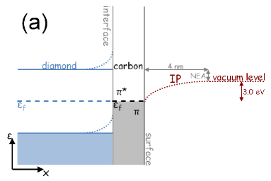
Panel (a) in the figure illustrates a case in which a GB of a lateral size of 1 nm is brought in contact with an intrinsic diamond grain of lateral size 10 nm. The Fermi level () in diamond is higher on the energy scale compared to that in carbon, which should result in a contact potential difference and upward band bending. As explained in great detail in Ref.[3], upon hydrogen termination of diamond, carbon supplies electrons which are liberated close to the triple graphite/diamond/vacuum interface having a reduced potential barrier suppressed by the induced NEA. When the graphitic patch size tends to an extremely small value at the limit, much smaller than the surrounding diamond host, the whole patch should reduce the potential barrier by a number close to the NEA value of diamond (from 4.6 eV to 3.0 eV as found in Ref.[3]). The barrier height/emission threshold of 3.0 eV was later confirmed in both photo- and field-emission experiments conducted for the same undoped polycrystalline diamond [5]. In carbon, electrons fill the full band below its Fermi level and are ready for resonant tunneling.
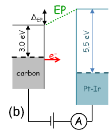
From the description of the TUNA tool, it follows that it is essentially a Kelvin probe in which the distance between the sample and the reference counter electrode () can be controlled with superfine precision and accuracy, and the surface topography can be recorded along with tunnel current maps. The panel (b) in the figure illustrates the energy balance diagram in the Kelvin probe method. For two separated conductive materials, vacuum levels are equal while Fermi levels are located below the vacuum level by values equal to respective work functions. When two separated samples are connected at the back through a voltage source, Fermi levels can be moved up and down with respect to each other. Electric potential difference is induced when energy position of the Fermi levels differ. is maximal and equal to 2.5 eV=5.5 eV3.0 eV when the Fermi levels in carbon and are equilibrated, while it is zero when vacuum levels are equilibrated (i.e. when the electrodes are disconnected); varies between 0 eV and 2.5 eV with applied voltage . In the TUNA experiment, voltage spanning +1 mV to +1 V was applied to the reference electrode, meaning its Fermi level was always lower than that of carbon by 1 meV to 1 eV. Thus, electrons flow from the sample to the electrode, i.e. in the direction coincidentally equivalent to the field emission case. Increase in the reading current should be observed when increasing the voltage applied to the counter electrode. Such increase was indeed observed. Current grew by a factor of 100 (few pA to few 100’s of pA) when the voltage was varied by a factor of 1,000 (1 mV to 1 V). This dependence is entirely different compared to the field emission mechanism of tunneling through a triangle barrier described by the Fowler-Nordheim formula. The barrier in the TUNA scheme has a different configuration. At a short range of a few nm, an electron experiences the image potential (), which grows from the Fermi level to the global asymptotic vacuum level as
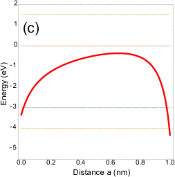
where is the electron charge and is the vacuum permittivity. In this case, we set the image potential growth scale to 4 nm. At distances farther than 4 nm, the image potential level is less than 0.1 eV below the vacuum level, meaning these potentials merge and become indistinguishable. With the tip placed at =1 nm, the resulting barrier will be formed and modified with the sum of the ’s of the two electrodes (intercepted at a scale where the is lower than the asymptotic vacuum level) and the (depends on the original Fermi level positions in the electrodes prior to connecting, and the voltage applied between the electrodes). An exemplary resulting barrier shown in the panel (c) is for the case with +1 V applied to the electrode: =1.5 eV and of is 1 eV below that of the carbon patch. Here, the zero energy level is set as the vacuum level on the carbon contact side. The resulting barrier is the sum of , , and electric potential . In this representation current growth, measured by TUNA, is simply proportional to the number of states in available for tunneling, as the Fermi level in the counter electrode slides down with increasing applied voltage. There is some likelihood that the versus behavior is non-monotonic because simultaneously more states in open up and the resulting barrier height and width are reduced. Carrier depletion in the carbon patch/GB could be another effect.
The TUNA results placed into context of the graphitic patch model make sense. In turn, observation of electron emission in insulating polycrystalline diamond can be only explained by the presence of conductive inclusions, i.e. GBs, because electrons in diamond grains are bound. If TUNA experiments were carried out away from the sample edges, it suggests GBs are electrically connected via some mechanism. The observed steady increase in surface emitting area from undoped MCD, to NCD, to UNCD (Fig.1 in Ref.[1]) should be caused by the increased ratio of graphitic phase (GB) to diamond phase (grain). In terms of emitting area, -doped NCD did not differ from UNCD since nitrogen is incorporated into GBs changing their size insignificantly compared to the size of surrounding grains. Further, the surge in the emitting area in - and -doped MCD films can be explained by actual grain doping that takes place so that GBs and grains become conductive and have impurity state bands able to supply electrons.
Similar situation seems to take place in case of scanning tunneling microscopy (STM) measuring electron emission properties of UNCD with embedded metallic nanoparticles [6]. From actual field emission data, it is seen that the ratio of the barrier height to the field enhancement factor, , in the exponent of the Fowler-Nordheim equation almost did not change, while the current density scaled-up significantly. It means that it is quite possible that enhanced emission properties are due to increased electron density introduced by the metallic nanoparticles (especially in the case of Au) and a larger phase distribution network boosted by the Au implantation. Additional confirmation by STM that Au nanoparticles produce measurable current alongside with GBs suggests that Au particles have a vast amount of electrons that can readily tunnel under a barrier produced by the sample surface and the counter electrode tip of an STM tool, situation equivalent to TUNA.
Another important consequence of the TUNA observations is that it rules out the assumption that the field enhancement factor of pure geometrical nature plays significant role in field emission, because electrons originate from GB topographical valleys. One way to design an alternative was proposed by Robertson [7], who illustrated a mechanism of self-focusing electric field lines at the hydrogen-terminated/unterminated discontinuities on the ideal planar surface giving rise to electric gradients 1 GV/m. Yet another possible way to introduce a of quasi-geometrical nature is as follows. In any undoped polycrystalline diamond or in incorporated NCD and UNCD, grains stay insulating. This means that nothing prevents electric field from penetrating through dielectric grains and focusing on conductive GBs (roughly of a shape of a blade as can be assumed from top-view and cross-section TEM images [8,9]). Such effect would be (relative permittivity of diamond) times smaller as compared to the case of the identical conductive blades placed in an external electric field in vacuum with . Overall such effect is modest, and field enhancement should not go over . Nevertheless, it is enough to reasonably account for found in experiments - see for instance updoped unterminated case for MCD in Ref.[5] showing . In polycrystalline diamonds where actual doping of grains can be achieved, such effect would vanish because the whole surface becomes conductive and the electric lines would terminate on the surface perpendicularly, meaning .
This means the potential barrier has to be the key to field emission in this class of materials. Improved emission properties of polycrystalline diamonds, especially upon doping/incorporation and termination/functionalization, mean the barrier height of the GB may reduce further from 3.0 eV to a lower number (1 eV). Mechanisms responsible could be the significant stress present in polycrystalline films [10], changing the absolute energy position of the Fermi level, and/or structural or chemical reconfigurations. As an example of the latter, in amorphous hydrogenated carbon nitride, a sister system to the GB material [11], barriers as low as 0.7 eV were observed [12]. The described and/or some other mechanisms acting synergistically could produce a surface barrier of a modified shape that enhances the tunneling current significantly.
To conclude, while scanning probe microscopy and field emission schemes are not directly equivalent, tunneling measurements help better understand and interpret field emission data taken for a parent (undoped, unterminated) polycrystalline diamond and field emission property changes upon bulk and surface modification of the same parent material. In various CVD diamond types with varied doping level/type and grain/GB size, taking advantage of the unique TUNA capabilities one could measure the surface barrier structure and Fermi level position using different potentials and polarities of the reference tip, inter-electrode separation and additional sample excitations. The electron supply function of a GB, i.e. electrons per emitting site and emission rate, density of states (cmeV-1), and conductivity mechanism through GBs could be also determined.
We thank Paul Schoessow for his help with the manuscript.
References
- (1) R. L. Harniman, et al., Carbon 94, 386 (2015).
- (2) V. Chatterjee, et al., Appl. Phys. Lett. 104, 171907 (2014).
- (3) J. B. Cui, et al., Phys. Rev. B 60, 16135 (1999).
- (4) To avoid any confusion, in what follows we use a more general term potential barrier to describe the penalty for an electron to escape into vacuum.
- (5) J. B. Cui, et al., Diamond Relat. Mater. 9, 1143 (2000).
- (6) K. J. Sankaran, et al., ACS Appl. Mater. Interfaces 6, 4911 (2014).
- (7) J. Robertson, J. Vac. Sci. Technol. B 17, 659 (1999).
- (8) O. A. Williams, Diamond Relat. Mater. 20, 621 (2011).
- (9) S. Turner, et al., Nanoscale 4, 5960 (2012).
- (10) H. Li, et al., J. Appl. Phys. 100, 094309 (2006).
- (11) M. Nesladek, et al., Phys. Rev B 54, 5552 (1996).
- (12) H. Saitoh, et al., J. J. Appl. Phys. 41, 6169 (2002).