The granularity effect in amorphous InGaZnO4 films prepared by rf sputtering method
Abstract
We systematically investigated the temperature behaviors of the electrical conductivity and Hall coefficient of two series of amorphous indium gallium zinc oxides (a-IGZO) films prepared by rf sputtering method. The two series of films are 700 nm and 25 nm thick, respectively. For each film, the conductivity increases with decreasing temperature from 300 K to , where is the temperature at which the conductivity reaches its maximum. Below , the conductivity decreases with decreasing temperature. Both the conductivity and Hall coefficient vary linearly with at low temperature regime. The behaviors of conductivity and Hall coefficient cannot be explained by the traditional electron-electron interaction theory, but can be quantitatively described by the current electron-electron theory due to the presence of granularity. Combining with the scanning electron microscopy images of the films, we propose that the boundaries between the neighboring a-IGZO particles could make the film inhomogeneous and play an important role in the electron transport processes.
Amorphous indium gallium zinc oxide (a-IGZO), which simultaneously possesses high optical transparency in visible range, high carrier mobility and low temperature fabrication process, is being considered as the good candidate of the active channel material in thin-film transistors (TFTs).zhang1 ; zhang2 ; zhang3 ; zhang4 Compared with polycrystalline metal oxides, the amorphous oxides do not have grain boundary. The grain boundary could seriously affect the carrier mobility and uniformity of oxide materials, which in turn would influence the performance of TFTs.zhang2 ; zhang4 ; zhang5 ; zhang6 Hence the amorphous oxide material is more suitable for TFTs than the polycrystalline one. However, even for the amorphous film, it often experiences the discontinuous to continuous process in the first stage of film growth. Thus the boundaries between amorphous particles are also inevitable in the amorphous films. In this Letter, we measured the variations in resistivity and Hall coefficient with temperature for the thick (700 nm) and thin (25 nm) a-IGZO films from 300 down to 2 K. We found the electron-electron interaction (EEI) due to the presence of granularity governs the temperature behaviors of longitudinal and Hall transport of the a-IGZO films. Combining the scanning electron microscopy (SEM) images of the films, we conclude that the subtle influence of boundaries between the the neighboring amorphous particles in a-IGZO films on the electronic transport processes can not be neglected.
The samples were deposited on glass substrates by rf sputtering method. A commercial InGaZnO4 ceramic target with purity of 99.99 was used as the sputtering source. The atomic ratio of In, Ga, and Zn is . The base pressure of the sputtering chamber was below Pa. The sputtering was carried out in an argon (99.999% in purity) atmosphere with the pressure of 0.6 Pa, and the sputtering power was maintained at 100 W during the deposition process. To obtain films with high conductivity, the substrate temperature was set as 688 and 788 K, respectively. We deposited IGZO films with thickness 700 and 25 nm at each deposition temperature. The film notations are listed in Table 1. Hall-bar-shaped samples were deposited for the measurements of Hall coefficient and conductivity , by using mechanical masks. The thicknesses of the films were measured with a surface profiler (Dektak, 6 M) for those films with thickness of 700 nm, and with the low-angle x-ray diffraction for those films with thickness of 25 nm, respectively. The crystal structures of the films were measured by using a x-ray diffractometer (XRD, D/MAX-2500v/pc, Rigaku) with Cu Kα radiation. The results indicate that all films are amorphous. The surface morphologies of the films were characterized by the SEM (S-4800, Hitachi). The electrical conductivity and Hall effect were measured using a physical property measurement system (PPMS-6000, Quantum Design), by employing the standard four-probe method. The aluminium electrodes with thickness 280 nm were deposited before the electrical transport property measurements.
| Film | |||||||||
|---|---|---|---|---|---|---|---|---|---|
| No. | (K) | (nm) | (K) | ( S) | (K) | ( m-3) | ( J) | ||
| 1 | 688 | 653.5 | 25 | 5.05 | 17.3 | 45 | 1.04 | 1.38 | 7.07 |
| 2 | 788 | 683.7 | 30 | 4.90 | 15.5 | 45 | 1.00 | 1.24 | 7.07 |
| 3 | 688 | 24.5 | 15 | 7.00 | 11.6 | 40 | 1.73 | 1.51 | 5.07 |
| 4 | 788 | 25.6 | 15 | 4.42 | 7.2 | 35 | 1.10 | 1.29 | 4.36 |
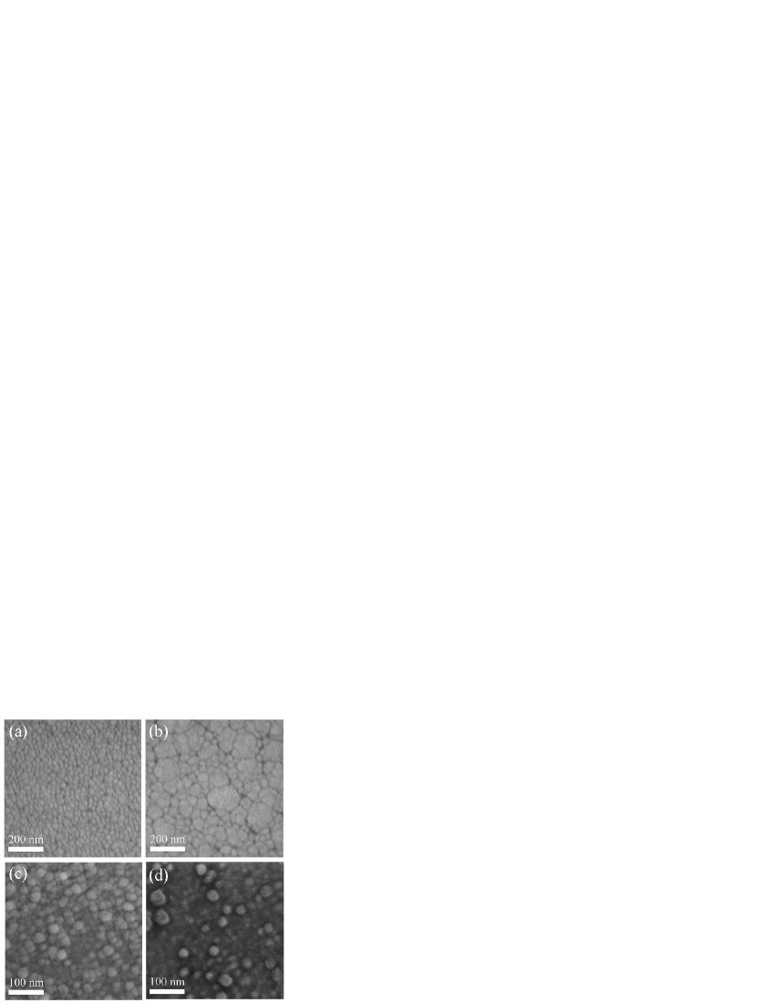
Figure 1 shows the SEM images of the films. Although these IGZO films are amorphous, they are composed of amorphous IGZO particles. For those 700 nm thick films, the mean particle size of the film deposited at 788 K is significantly larger than that of the film deposited at 688 K. In addition, there are distinct boundaries between the neighboring particles. These boundaries could affect the uniformity as well as the subtle electron transport processes of the amorphous films.
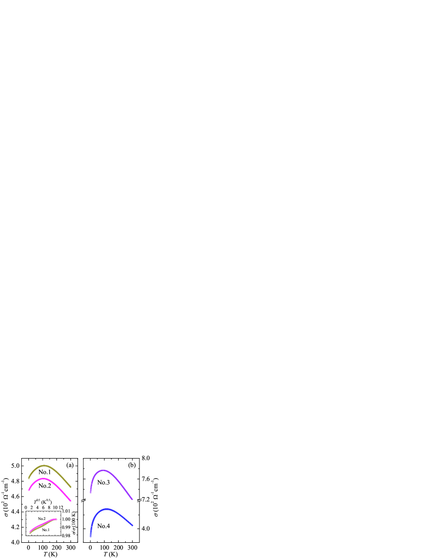
Figure 2 shows the conductivity varies as a function of temperature from 300 down to 2 K for the films. The room temperature conductivities of the films lie between and cm-1. Hence all the films have relative high conductivity. Upon decreasing temperature from 300 K, the conductivity of each film increases with decreasing temperature, reaches its maximum at ( varies from 92 to 115 K for our films), and then decreases with further decreasing temperature. The enhancement of conductivity with decreasing temperature above indicates that these a-IGZO films possess metal (more strictly, degenerate semiconductor) characteristics in transport properties.zhang7 ; zhang8 The reasons why the a-IGZO films have the metal-like transport properties deserve further investigation. In homogeneous disordered conductors, the decrease of conductivity with decreasing temperature at liquid helium temperatures generally originates from the weak-localization (WL) and EEI effects.zhang9 ; zhang10 ; zhang11 ; zhang12 ; zhang13 ; zhang14 In three dimensional disordered conductors, the corrections to the conductivity due to WL and EEI effect are given aszhang12 ; zhang13 ; zhang14
| (1) |
where is a constant, is the electronic charge, is the Planck constant divided by , is the Boltzmann constant, is the diffusion constant, is electron dephasing time, is the the screening factor averaged over the Fermi surface. The first term on the right hand side of Eq. (1) arises from the WL effect, while the second term originates from the interaction effect. To determine independently, we measured the conductivity varies as a function of temperature under a magnetic field of 7 T, which is plotted in the inset of Fig. 2. Since the WL effect would be suppressed by the high field,zhang12 ; zhang14 one would expect that the conductivities vary linearly with at low temperature regime. However, the law is not observed in the inset of Fig. 2, which means other mechanisms should govern the temperature behavior of conductivity at liquid helium temperatures.
As mentioned above, there are distinct boundaries between the neighboring a-IGZO particles. The conductivities of the boundaries would be much less than that inside of the particles. Thus the low temperature conduction processes of the a-IGZO films would be similar to that of granular metals, where a granular metal means a metal-dielectric composite lying above the percolation threshold.zhang15 ; zhang16 ; zhang17 According to the recent theories, the EEI effect in granular metals is distinct from that of homogeneous disordered conductors. Specifically, in granular metals and the strong intergrain coupling limit [1, where is the dimensionless intergranular tunneling conductance, is the intergrain tunneling conductance], the conductivityzhang17 ; zhang18 ; zhang19 ; zhang20 and Hall coefficientzhang21 ; zhang22 can be written as
| (2) |
and
| (3) |
where is the effective carrier concentration, is a numerical lattice factor, is the mean level spacing in the metallic particle, is the charging energy, =, and is the Thouless energy, is the conductivity without the Coulomb interaction, and is the dimensionality of the granular array. Eq. (2) is valid in the temperature range , while Eq. (3) is valid in . Recently, the validity of Eq. (2)zhang23 ; zhang24 ; zhang25 ; zhang26 ; zhang27 ; zhang28 ; zhang29 ; zhang30 ; zhang31 and Eq. (3)zhang28 ; zhang29 ; zhang30 ; zhang31 has been experimentally tested.
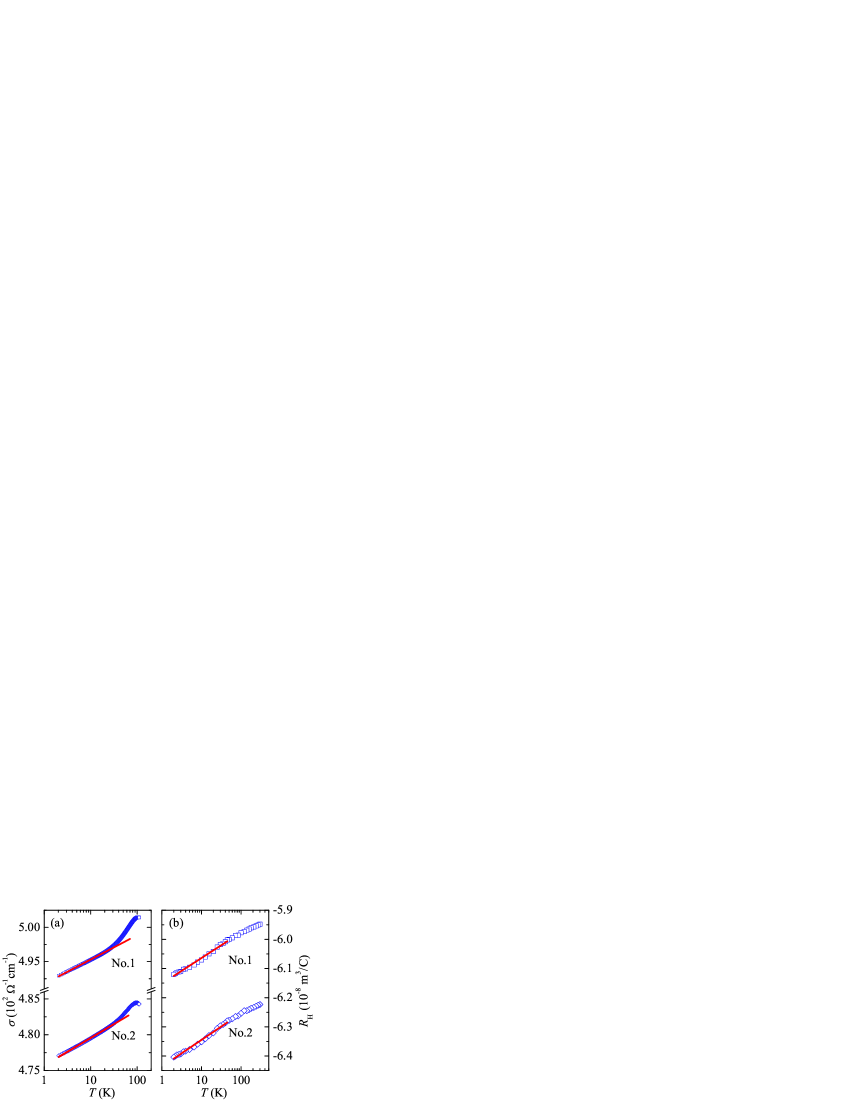
Figure 3 (a) and 3 (b) show the conductivities and Hall coefficients of the nm thick films variation with temperature at low temperature regime. Clearly, the conductivity (Hall coefficient) varies linearly with logarithmic temperature from 2 (2) to 25 K (45 K) for each film. The experimental () versus () data are least-squares fitted to Eq. (2) [Eq. (3)], and the results are plotted as solid curves in Fig. 3 (a) [Fig. 3 (b)]. When comparing the - data with Eq. (2), and are set as the adjustable parameters and the charging energy is taken to be , where K is the maximum temperature below which the law holds.zhang23 ; zhang28 For the - fitting processes, and are the adjustable parameters, has been independently determined above, and is taken the value of carrier concentration at ( is the maximum temperature below which varies linearly with ). The obtained fitting parameters, together with the basic parameters of sample No.1 and No.2 are listed in Table I. From Table I, one can see that the values are far greater than 1. Hence the necessary condition () for the validity of Eqs. (2) and (3) is satisfied.zhang17 ; zhang23 In addition, the extracted values are close to 1 (more precisely, slightly greater than 1), which is consistent with the theoretical prediction.zhang23 ; zhang26 The obtained values of are also reasonable. Hence Eqs. (2) and (3) are safely applicable for films No.1 and No.2.
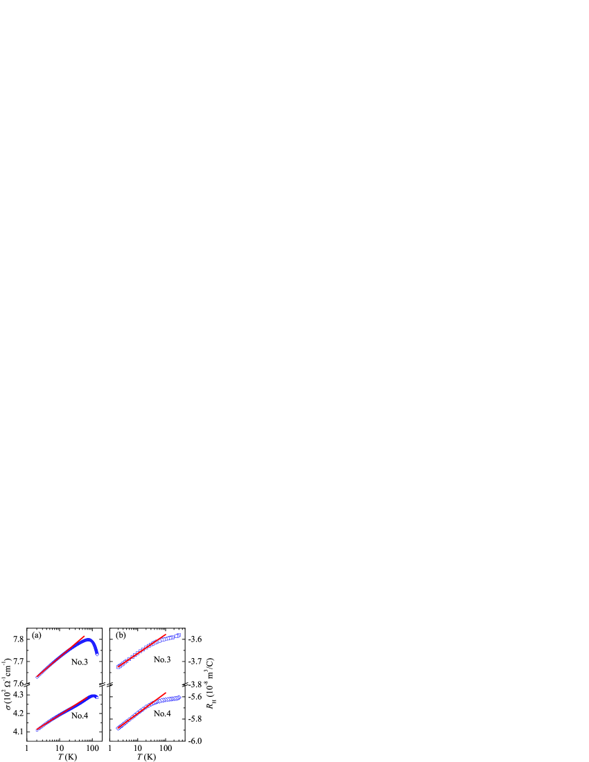
Figure 4 (a) and 4 (b) show variations of conductivity and Hall coefficient with temperature for the two 25 nm, thin films, respectively. Clearly, both the conductivity and Hall coefficient vary linearly with at low temperature regime. Inspection of Eqs. (2) and (3) indicates that the behaviors of and are independent of the granular array dimensionality. From the SEM images, one can see that the a-IGZO particle size lies between 20 and 30 nm, thus it is reasonable to assume that the 25 nm films are covered by only one layer of a-IGZO particles. Here we treat the 25 nm films as two-dimensional (2D) granular arrays [ in Eq.(2)]. The experimental and data are least-squares fitted to Eq.(2) and Eq.(3), respectively, and the results are shown as solid curves in Fig.4. The detailed fitting processes are identical to that used in 700 nm films. The obtained values of parameters , , and are listed in Table 1. The values of the parameters are also reasonable.
In 2D disordered homogeneous conductors, the EEI effect can also cause a correction to the conductivity. Specifically, the change of the sheet conductivity can be written aszhang14 ; zhang32
| (4) |
where is an arbitrary reference temperature, is the electron screening factor. The data in Fig. 4 (a) are also compared with Eq. (4). Certainly, the experimental data follow the predication of Eq. (4). However, the least-squares fits would lead to positive values for both films ( and for films No.3 and No.4, respectively). For the 2D disordered homogeneous conductor, the electron screening factor is required .zhang9 Thus the measured cannot be ascribed to the conventional EEI effect being applicable to the disordered homogeneous conductor. This result, on the other side, indicates that the boundaries between the neighboring a-IGZO particles play an important role in the electron transport processes.
In summary, we deposited 700 nm and 25 nm a-IGZO films by rf-sputtering methods. The SEM images indicated the films are composed of a-IGZO particles and there are distinct boundaries between neighboring particles. All films reveal metallic characteristics in electron transport properties. At low temperature regime, both the conductivity and Hall coefficient vary linearly with , which cannot be explained by the traditional EEI effect. We found that these behaviors of and result from the EEI effect due to the presence of granularity. The subtle inhomogeneity of the a-IGZO is caused by the boundaries between neighboring amorphous particles.
This work was supported by The National Basic Research Program of China through Grant No. 2014CB931703, the NSF of China through Grant No. 11174216, and Research Fund for the Doctoral Program of Higher Education through Grant No. 20120032110065.
References
- (1) K. Nomura, H. Ohta, A. Takagi, T. Kamiya, M. Hirano, and H. Hosono, Nature 432, 488 (2004).
- (2) T. Kamiya, K. Nomura, and H. Hosono, Sci. Technol. Adv. Mater. 11, 044305 (2010).
- (3) H. Yabuta, M. Sano, K. Abe, T. Aiba, T. Den, H. Kumomi, and H. Hosono, Appl. Phys. Lett. 89, 112123 (2006).
- (4) T. Kamiya, K. Nomura, and H. Hosono, J. Disp. Technol. 5, 273 (2009).
- (5) C. Kim, S. Kim and C. Lee, Jpn. J. Appl. Phys. 44, 8501 (2005).
- (6) K.Nomura,H. Ohta, K. Ueda, T. Kamiya, M. Hirano, and H. Hosono, Science 300, 1269 (2003).
- (7) J. M. Ziman, Electrons and Phonons (Clarendon Press, Oxford, 1960), p.364.
- (8) C. Kittel, Introduction to Solid State Physics, 7th ed, (Wiley, New York, 1996).
- (9) B. L. Altshuler and A. G. Aronov, in Electron-Electron Interactions in Disordered Systems, edited by A. L. Efros and M. Pollak (Elsevier, Amsterdam, 1985).
- (10) G.Bergmann, Int. J. Mod. Phys. B 24, 2015 (2010).
- (11) G.Bergmann, Phys. Rep. 107 (1984) 1.
- (12) B. L. Altshuler, D. Khmelnitzkii, A. I. Larkin, and P. A. Lee, Phys. Rev. B 22, 5142 (1980).
- (13) S. P. Chiu, J. G. Lu, and J. J. Lin, Nanotechnology 24, 245203 (2013).
- (14) P. A. Lee and T. V. Ramakrishnan, Rev. Mod. Phys. 57, 287 (1985).
- (15) P. Sheng, Philos. Mag. B 65, 357 (1992).
- (16) B. Abeles et al., Adv. Phys. 24, 407 (1975).
- (17) K. B. Efetov and A. Tschersich, Europhys. Lett. 59, 114 (2002).
- (18) K. B. Efetov and A. Tschersich, Phys. Rev. B 67, 174205 (2003).
- (19) I. S. Beloborodov, K. B. Efetov, A. V. Lopatin, and V. M. Vinokur, Phys. Rev. Lett. 91, 246801 (2003).
- (20) I. S. Beloborodov, A. V. Lopatin, V. M. Vinokur, and K. B. Efetov, Rev. Mod. Phys. 79, 469 (2007).
- (21) M. Y. Kharitonov and K. B. Efetov, Phys. Rev. Lett. 99, 056803 (2007).
- (22) M. Yu. Kharitonov and K. B. Efetov, Phys. Rev. B 77, 045116 (2008).
- (23) L. Rotkina, S. Oh, J. N. Eckstein, and S. V. Rotkin, Phys. Rev. B 72, 233407 (2005).
- (24) P. Achatz, W. Gajewski, E. Bustarret, C. Marcenat, R. Piquerel, C. Chapelier, T. Dubouchet, O. A. Williams, K. Haenen, J. A. Garrido, and M. Stutzmann, Phys. Rev. B 79, 201203 (2009).
- (25) Y. C. Sun, S. S. Yeh, and J. J. Lin, Phys. Rev. B 82, 054203 (2010).
- (26) R. Sachser, F. Porrati, C. H. Schwalb, and M. Huth, Phys. Rev. Lett. 107, 206803 (2011).
- (27) F. Porrati, R. Sachser, C. H. Schwalb, A. S. Frangakis, and M. Huth, J. Appl. Phys. 109, 063715 (2011).
- (28) Y. J. Zhang, Z.Q. Li and J. J. Lin, Phys. Rev. B 84, 052202 (2011).
- (29) Y. Yang, Y. J. Zhang, X. D. Liu, and Z. Q. Li, Appl. Phys. Lett. 100, 262101 (2012).
- (30) Y. J. Zhang, K. H. Gao, and Z. Q. Li, Appl. Phys. Lett. 106, 101602 (2015).
- (31) Y. N. Wu, Y. F. Wei, Z. Q. Li, and J. J. Lin, Phys. Rev. B 91, 104201 (2015).
- (32) B. L. Altshuler, A. G. Aronov, and P. A. Lee, Phys. Rev. Lett. 44, 1288 (1980).