Electrically-induced phase transition in -(BEDT-TTF)2I3:
Indications for high-mobility hot charge carriers
Abstract
The two-dimensional organic conductor -(BEDT-TTF)2I3 undergoes a metal-insulator transition at K due to electronic charge ordering. We have conducted time-resolved investigations of its electronic properties in order to explore the field- and temperature-dependent dynamics. At a certain threshold field, the system switches from low-conducting to a high-conducting state, accompanied by a negative differential resistance. Our time-dependent infrared investigations indicate that close to the strong electric field pushes the crystal into a metallic state with optical properties similar to the one for . Well into the insulating state, however, at K, the spectral response evidences a completely different electronically-induced high-conducting state. Applying a two-state model of hot electrons explains the observations by excitation of charge carriers with a high mobility. They resemble the Dirac-like charge-carriers with a linear dispersion of the electronic bands found in -(BEDT-TTF)2I3 at high-pressure. Extensive numerical simulations quantitatively reproduce our experimental findings in all details.
pacs:
71.30.+h, 71.45.-d, 72.90.+y, 72.40.+wI Introduction
The charge-transfer salt -(BEDT-TTF)2I3 is probably the best studied model compound of a metal-insulator transition in two-dimensional electron systemsBender et al. (1984a); Dressel et al. (1994) that is supposed to be driven by electronic charge order.Kino and Fukuyama (1995, 1996); Seo et al. (2004) From NMRTakano et al. (2001); Takahashi et al. (2006) and optical spectroscopy,Moldenhauer et al. (1993); Wojciechowski et al. (2003); Dressel and Drichko (2004); Yue et al. (2010); Ivek et al. (2011); Yakushi (2012) as well as x-ray diffraction studiesKakiuchi et al. (2007) it is well known that below K charge disproportionation develops on the BEDT-TTF molecules. Since its discovery three decades ago, the intererst in the title compound never faded because it exhibits a rich temperature-pressure phase diagram, with a number of intriguing quantum phenomena ranging from electronic ferroelectricityIvek et al. (2010); Tomić and Dressel (2015); Lunkenheimer et al. (2015) to superconductivity,Tajima et al. (2002); Kobayashi et al. (2004) from nonlinear transportDressel et al. (1995); Ivek et al. (2012) to zero-gap semiconductivityTajima et al. (2006); Mori (2010) characterized by Dirac cones and massless Dirac fermions,Tajima et al. (2007); Suzumura and Kobayashi (2012); Kajita et al. (2014); Beyer et al. (2016) but also the appearance of persistent photoconduction,Tajima et al. (2005) photoinduced phase transition,Iwai et al. (2007); Kawakami et al. (2010); Iwai (2012) and nonlinear ultrafast optical response.Yamamoto et al. (2008)
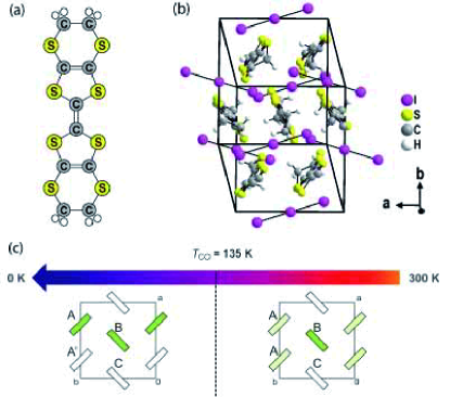
At room temperature -(BEDT-TTF)2I3 consists of layers formed by the BEDT-TTF molecules that are separated along the -direction by I anions creating an electronically two-dimensional system, as displayed in Fig. 1. At K the symmetry class of the crystal changes from P to P1 at low temperatures, thus breaking the inversion symmetry between the molecules A and A′. Now, all four molecules are crystallographically independent and each molecule in the unit cell carries a distinct charge different from the others. As shown in Fig. 1(c), the charge order forms horizontal stripes with molecule B still being charge-rich and molecule C charge-poor, but either molecule A or A′ being charge poor/rich. The charge ordering leads to a ferroelectric state which was probed by second harmonic generation of lightYamamoto et al. (2008, 2010, 2012) as a direct proof of the loss of the inversion symmetry. These studies have also shown that different ferroelectric domains exist in a single crystal separated from each other by domain walls. Indications of an influence of cooling rate and pressure on the amount of domains and their size was found, although a systematic study is still missing and necessary.
Recent dielectric measurementsIvek et al. (2010, 2011) detect two modes with a dielectric strength between 400 and 5000 for the - and -direction indicating a strong ferroelectric response with no temperature dependence below . The first mode is present at all temperatures and is ascribed to a charge-density wave, which is screened by activated charge carriers since the relaxation time follows the temperature-dependence of the dc conductivity. The second mode appears on further cooling below K. It is suggested that this response is caused by solitons and domain walls which are fixed to pinning centers. Alternatively the existence of polar and nonpolar stacks of the BEDT-TTF molecules was suggested,Lunkenheimer et al. (2015) preventing long-range ferroelectricity.
In a complementary approach, the electrodynamical properties of -(BEDT-TTF)2I3 at the metal-insulator phase transition have been explored by non-linear and time-dependent studies.Naito (2010); Iimori and Ohta (2014) Particular attention was drawn by the observation of photo-induced phase transition phenomena,Iwai et al. (2007); Nakaya et al. (2008); Kawakami et al. (2010) photoconductivityTajima et al. (2005); Iimori et al. (2009) connected with a memory effect,Iimori et al. (2007a, b) non-linear conductivityDressel et al. (1994); Tamura et al. (2010); Ivek et al. (2012) and zero-gap states under pressure.Katayama et al. (2006); Mori (2010); Alemany et al. (2012); Beyer et al. (2016) Here we focus on the electrically-induced phase transition in -(BEDT-TTF)2I3 by investigating the time-resolved transport and optical properties. We then apply a model of non-equilibrium charge carriers to our observations explaining our findings in all details.
II Experimental Results
The time-, temperature- and field-dependent transport and optical studies have been conducted on -(BEDT-TTF)2I3 single crystals, as grown by electrochemical methods.Bender et al. (1984a, b) The experimental details are given in the Supplemental Materials.SM
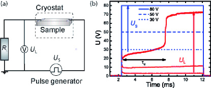
Besides conventional dc transport measurements in four-point geometry (cf. Figs. S1 and S2), dynamical resistivity studies have been performed by applying a voltage of across the single crystal of -(BEDT-TTF)2I3 for a few milliseconds and measuring the total current flow as a function of time. In the metallic but also well into the insulating state, the response is basically constant at low voltage, indicating a steady state. In Fig. 2(b) it can be seen, however, that for V applied at low temperatures ( K, for instance), heating continuously increases the current until the sample suddenly turns metallic at certain delay time . In a first step (Sec. II.1) we want to characterize, how this switching evolves with time and how the behavior depends on temperature and electric field applied. In Sec. II.2 we will then present optical investigations which elucidate the nature of the electrically-induced metallic state.
II.1 Transport Studies
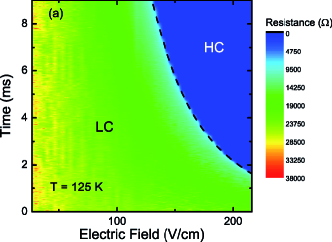
In Fig. 3 the time dependence of the sample resistance is plotted as a function of the applied electric field for two selected temperatures. At K the sample resistance is approximately 19 k. In time frame under inspection it jumps abruptly from the insulating state into a high-conducting state above a certain threshold field that is marked by the color change from green to blue in Fig. 3. The resistance is reduced by two orders of magnitude to . For the contour plot it becomes clear that the switching takes place with a certain delay time , which decreases with increasing electric field in a nonlinear manner.
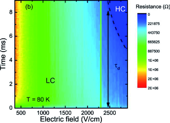
For lower temperatures, K, the behavior is rather similar; however, the total resistance is much higher and decreases slightly with increasing voltage due to the nonlinear behavior of the contact resistance.Ivek et al. (2012) Note that at reduced temperatures the electric field must be significantly increased to induce the high conducting state. It should also be pointed out that despite the different absolute values of resistivity recorded, the step height between low- and high-conducting range is again about two orders of magnitude, as in the case of K.
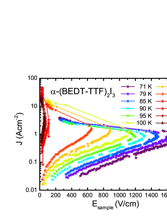
The calculated current-voltage characteristic, vs. , is displayed in Fig. 4 for the temperature range from to 130 K. The curves exhibit a regime of a negative differential resistance (NDR), where the current jumps to a much larger value, while the electric field at the sample drops significantly. This curve reveals a so-called S-shape (current-controlled), in contrast to an N-curve (voltage-controlled) where the current drops to smaller values with increasing electric field due to a reduction of the carrier mobility. The NDR appears above a certain threshold field , which increases with lowering . Before the NDR regime the current density increases linearly reflecting ohmic behavior. In our context, this means that the conductivity must be significantly enhanced by generating high-mobility carriers.
From Fig. 4, we extract the threshold electric field and the threshold current density and plot the parameter as a function of temperature in Fig. 5(a). decreases linearly with up to where it vanishes, as expected; there is no NDR observed in the metallic state above . This agrees with measurements in the current mode performed in -(BEDT-TTF)2I3 below 100 K;Tamura et al. (2010); Itose et al. (2013) in other organic materials similar observations have been reported.Ozawa et al. (2009) There, the threshold field also rises continuously as is reduced.
Let us compare the absolute value of the NDR threshold fields found in our experiments to other systems. In the case of typical charge-density-wave materials,Grüner (1988) threshold fields below 1 V/cm are typically observed, while the electric field values we extract from -(BEDT-TTF)2I3 are several orders of magnitude larger. On the other hand, avalanche effects or dielectric breakdown are found in semiconductors or insulators only for fields exceeding 1 MV/cm. But also the observed temperature dependence is distinct from those phenomena. For a charge-density-wave the threshold-field follows a behavior,Maki (1986) in contrast to dielectric breakdown where it behaves like . The linear dependence observed here in -(BEDT-TTF)2I3 does not follow either of them. Hence we conclude that the nonlinear transport behavior in charge-ordered materials plays a special role and cannot be simply classified within the previous mentioned phenomena.
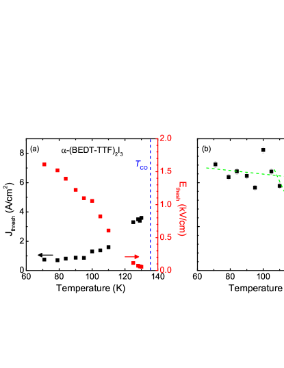
In contrast to , the current density does not follow a linear temperature behavior; it seems to diverge towards and approaches a constant value at low . Similar results have been reported previously.Itose et al. (2013) From both quantities, the power density at the threshold, , can be readily calculated [Fig. 5(b)]. Interestingly, the power necessary to the switch the conduction state rises steeply as the temperature drops below ; only for K remains basically constant. This temperature dependence resembles the behavior of the resistivity plotted in Fig. S2, where the largest modification occurs in a narrow temperature range K where the energy gap opens.
In order to ensure that this effect is not caused by Joule heating, we have conducted a thorough calculation of the stored energy and the possible temperature rise; details are given in the Supplemental Materials.SM Even under the assumption that 100% of the electrical power is used for heating the crystal, the experiments performed at K will never lead to sample temperatures above 96 K. At least far below K, we can therefore exclude that the switching from the low-conducting to high conducting state is caused by Joule heating.
II.2 Optical Studies
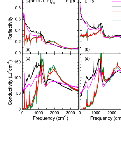
Beyond these time-dependent transport studies, more insight into the nature of the electronic state can be obtained from the frequency dependent conductivity.Dressel and Grüner (2002) It is well known that the metal-insulator transition of -(BEDT-TTF)2I3 at K has a strong influence on the optical response probed by polarized infrared reflection measurements. As illustrated in Fig. 6, the reflectivity decreases below approximately 1500 cm-1 when the temperature drops below , while increases in the mid-infrared region. The corresponding optical conductivity is plotted in Fig. 6(c) and (d), demonstrating the shift in spectral weight from the frequency range below the gap at approximately 600 cm-1 to the mid-infrared peak around 200 cm-1.Clauss et al. (2010) The change takes place within a rather narrow temperature interval between and 120 K with basically not variation below.
Since we are interested who the reflectivity changes in certain spectral regions, in Fig. 7 we plot the difference in reflectivity between various temperatures above and below . When comparing and 80 K, for instance, exhibits almost no modification besides a slight shift of the energy gap in the charge ordered phase. Pronounced spectral changes, however, are found between the two phases, i.e. looking at and 80 K. When entering the charge-ordered state below the low-frequency reflectivity rises on the expense of the mid-infrared region. No significant differences are observed between the two polarizations and .
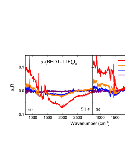
In order to characterize the electric-field-induced metallic state spectroscopically and to draw a more complete picture of the dynamics at the metal-insulator transition of -(BEDT-TTF)2I3, we have performed time-resolved infrared measurements by employing step-scan Fourier-transform infrared spectrometer Bruker Vertex 80v; for technical details see Ref. Pet, a. The time resolution was set to 20 s and 1000 time steps were recorded for 20 ms. The data were acquired 1 ms before the voltage pulse was initialized. To improve the signal-to-noise ration, we averaged over 20 scans. The spectral resolution was 4 cm-1 and the recorded frequency ranged from to 4000 cm-1. The time-resolved measurements were performed in the ac-mode, highlighting the changes in reflectivity as time elapses, where . It is of interest to compare this with the change of reflectivity when the temperature is varied with respect to a reference temperature : , as plotted in Fig. 7.
II.2.1 Close to metal-insulator transition: K
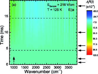
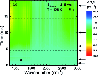
In Fig. 8 the time- and frequency-dependent change of the reflectivity at K is plotted as recorded for the - and -direction when an electric field of V/cm is applied parallel to the crystallographic -axis. Reflectivity data in the mid-infrared range are acquired during a period of 20 ms for both directions. After 1 ms the voltage pulse is applied to the sample, but it takes another few milliseconds before the reflectivity changes appreciably. Only 4 ms after the voltage pulse has started, increases for cm-1, which is accompanied by a drop of the signal between 1500 and 2500 cm-1. Qualitatively the behavior is similar for both directions. After the voltage pulse has stopped at ms, the signal keeps increasing almost to the end of the measurement window. The influence of the electric field on the material exceeds the pulse duration; any modification remains longer than the recorded time frame.
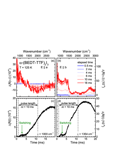
In order to analyze the time-dependence of the reflectivity in more detail, we take spectral and time slices at the position marked in Fig. 8 by black arrows. In panels (a) and (b) of Fig. 9 the evolution of the spectra is shown for six different points in time, ranging from to 18 ms. Before the pulse is applied (at ms), the reflectivity is steady. Immediately following the applied field, the reflectivity rises, but at 2 ms comes to a halt at a minuscule level where it stays until ms. From our time-resolved transport measurements presented in Fig. 3, we can extract that at K the electrically-induced switching occurs 1.7 ms after the field is applied. Thus we cannot relate the phase transition detected in the resistivity drop with the change of the reflectivity at 5 ms. We conclude two different effects being responsible for these observations. By taking a closer look at the spectral shape of after 5 ms and compare them with the reflectivity difference presented in Fig. 7, we immediately recognize the similarity in the difference spectra between and 80 K. In other words, the electric pulse transforms the crystal into the metallic phase after 4 ms.
These observations and conclusions are confirmed when we analyze the time-dependent behavior for two selected frequencies, and 1354 cm-1, plotted in Fig. 9(c) and (d). The signal starts to rise slightly with the onset of the voltage pulse, but it soon levels off. The electrically-induced switching point at ms is not reflected in the spectra. Only 4 ms after the voltage is applied, the reflectivity starts to rise linearly. This continues well beyond the endpoint of the pulse; saturates at about 15 ms and then decreases linearly. With slight variations the overall behavior is similar for both polarization directions.
Several peculiarities call for further discussion:
(1) We suggest that in the first 4 ms of the voltage pulse, a fraction of the sample is transferred into a metallic phase. This picture is supported by spatially-resolved Raman measurements of a current-induced phase transition under steady-state conditions.Mori et al. (2009) Mori et al. observed a modification of the spectral intensity of a emv-coupled mode of the BEDT-TTF molecules, which they ascribed to the variation of the electronic background and therefore to an electrically-induced metallic state. In contrast, a temperature-sensitive vibrational mode of the I anions does not reveal any modification. Note, however, that measurements under steady current flow are likely to be subject to heating.Zimmers et al. (2013) Since we cannot correlate the observed switching from a low- to high-conducting state to the temporal dynamics of the sample resistivity, we interpret the change of reflectivity by a thermally-induced phase transition of a few spatially limited areas. The electrical current is affected by some inhomogeneously distributed impurities and cracks within the sample leading to local heating.
(2) It is a remarkable fact that the sample is already in the highly conducting (metallic-like) state according to the transport measurements, but the reflectivity changes only after ms and grows further until 15 ms, although the pulse is already switched off at ms. We suggest that the system is in a highly-conducting state due to an excited electronic system. These “excited” or “hot” charge carriers couple to the lattice subsystem to which the energy is eventually transferred with a certain delay time. This leads to a heating-up of the sample across the phase transition causing the reflectivity change. Calculations of the heating effects confirm this picture.SM Here we assumed that the entire electric energy provided by the voltage pulse is completely converted into heat and the sample temperature exceeds .
(3) The excited charge carriers relax back to their initial ground state by releasing the energy to the crystal lattice. saturates when the energy transferred to the phonon bath is balanced by the outflow to the heat sink of the sample holder. Eventually all energy is stored in the lattice subsystem; without any influx the temperature rises leading to a linear drop of the reflected signal. This picture consistently explains also our electric pump-probe experimentsIvek et al. (2012) where the resistivity recovers in an exponential manner within a few milliseconds after the highly conducting state was initialized by a 3 ms long voltage pulse.
(4) The linear decrease in after 17 ms can be quantitatively described by Newton’s law of cooling , with is the thermal conductivity, denoting the environment temperature, and the temperature of the heated lattice. Due to the elevated temperature thermal radiation was neglected as a relevant factor.
II.2.2 Well below the metal-insulator transition: K
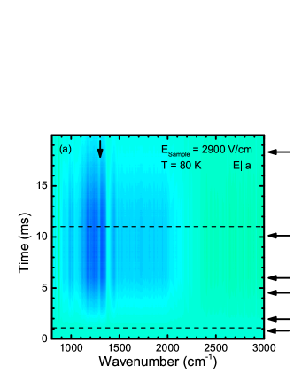
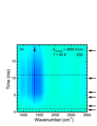
Now, we consider the switching behavior of -(BEDT-TTF)2I3 at K, i.e. at temperatures far below . The frequency- and time-dependent spectra are displayed in Fig. 10 for the polarizations and , under an electric field strength V/cm. The voltage pulse arrives at the sample at time 1 ms and lasts for 10 ms. In both spectra, a change of can be recognized right with the onset of the pulse. The important point is, however, that in contrast to the behavior at K depicted in Fig. 8, the reflectivity gets smaller and thus is mainly negative. It persists until the end of the record time, although it relaxes back about 4 ms after the voltage pulse has been switched off.
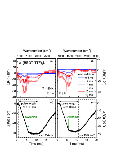
In Fig. 11 the frequency-dependent is plotted for different points in times, extracted as slices from Fig. 10. Immediately after the voltage pulse has arrived at 1 ms, the negative signal increases linearly, saturates at ms and eventually drops after 12.5 ms. For there seems to be one isosbetic point around 2300 cm-1, above that frequency develops similar, but with opposite, i.e. positive sign. For two frequencies can be identified, and 2650 cm-1, with basically no temporal development, but the changes are always negative. The spectra differ significantly from those recorded at K (Fig. 9) and are interpreted as a reduction of the electronic band and the emv-coupled modes in the case of the - and -direction, respectively. The comparison with the temperature modulated reflectivity shown in Fig. 7 reveals a small increase of the sample temperature of only a few Kelvin, for instance, from to 90 K. Since we do not observe a positive signal below 1000 cm-1, the energy gap does not shrink; in excellent agreement with our estimation of an upper limit of the sample temperature caused by Joule heating,SM which predicts a maximum temperature of 96.5 K in the high-conducting state, which is still far below K. Therefore, we believe that for our 80 K-experiments no thermally induced phase transition is responsible for the switching from the low-conducing to the high-conducting state.
The time evolution of at two frequencies is displayed Fig. 11(c) and (d). The signal decreases in a linear fashion right after the onset of the voltage pulse. Precisely at the resistivity switching from the low-conducting to the high-conducting state at ms the signal becomes constant, which implies that the energy flow is balanced between the electron system, the lattice and the environment. When the voltage pulse is turned off, the excited charge carriers of the electronic system, decays back, the energy is transferred to the lattice system. The infrared signal remains high, exceeding the duration of the applied voltage, before the lattice system is cooled down linearly in accordance with Newton cooling, as discussed above.
III Hot Electron Model
In order to explain our observations, we suggest a model of “hot” electrons or non-equilibrium charge carriers.Kroll (1974); Sze and Ng (2007); Yu and Cardona (2010) It assumes that the electric power is first stored in the electron system causing an increase of the electron temperature . The coupling to the lattice subsystem is responsible for heating up the lattice and to increase the lattice temperature . Two types of carriers are assumed with rather different mobilities. More details are presented in the Supplemental Materials.SM
III.1 Simulation of time dependence
The electron temperature can be calculated by considering energy conservation:
| (1) |
where describes the power gained by the electrons and corresponds to the energy transfer from the electrons to the lattice subsystemrem . We have solved Eq. (1) numerically by first calculating the right side and subsequently determining from the left side for each time step of the voltage pulse. The electrical conductivity is taken from dc measurements plotted in Fig. S2; the load resistance was experimentally selected between 1 k and 100 k. In addition we choose an electronic heat capacity and thermal conductivity of the electron system in agreement with previous investigations, where a similar two-state model was applied to other low-dimensional organic conductors.Mori et al. (2009); Ozawa et al. (2009)
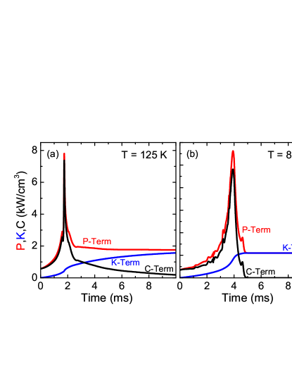
In Fig. 12 the time dependences of the -, -, and -terms are plotted for and 80 K. The electric power is transferred to the electronic system right from the beginning of the voltage pulse. The cooling term, however, increases only slowly for the elevated temperature K. Before the switching point, the electric power as well as the stored energy in the electric system diverge and drop afterwards to a fixed value. The -term decreases slowly to zero since the cooling term approaches the electric power term initializing the steady-state. At low temperatures, K, the power term behaves similarly, only the cooling term immediately after the resistivity switching reaches the value of the electric input -term; correspondingly no energy is then transferred to the electronic system.
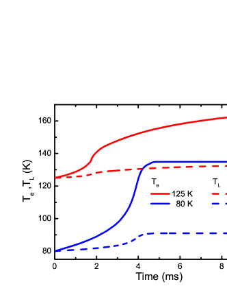
The time evolution of the electron temperature is displayed in Fig. 13 for the two experiments at different temperatures. When starting at K, the electron temperature increases more than linearly, then reveals a step-like feature at the phase transition around 2 ms and finally increases sub-linearly up to 160 K at the end of the pulse. For the low-temperature experiment ( K) the temperature rises steeply up to K and stays constant; right below the transition temperature .
The total heat capacityFortune et al. (1991) of -(BEDT-TTF)2I3 crystals below , , is more than five times larger than the values for the electron system used in our simulations. This agrees well with the fact, that phonon typically dominate above 10 K due to the power-law of the lattice contribution compared to the linear dependence of the electronic heat capacity. Assuming that both contributions are independent and add up, , energy conservation yields:Mori et al. (2009) and thus
| (2) |
with the initial environmental temperature ; here is the effective electron temperature and denotes the lattice temperature due to heating.
Using Eq. (2) we estimate the time dependence of the lattice temperature of -(BEDT-TTF)2I3 for and 80 K and display the results in Fig. 13. Trailing the electron temperature, the lattice temperature increases only slightly from to 132 K within the pulse duration of 10 ms; hence it stays below the charge-ordering temperature of K. Of course, we cannot exclude that due to some scattering centers can locally exceed the transition temperature. We now understand, why the reflectivity still increases after switching to the high-conducting state; the lattice temperature keeps rising well after the system has switched. From Fig. 9 we clearly see a metallic transition in the 125 K run, but at K the reflectivity variation indicates only a small increase of of less than 10 K. This is exactly what our simulation reproduce: the lattice temperature first increases but then saturates as the system switches from the low-conducting to the high-conducting state. This explains why remains constant in time until the pulse is switched off.
III.2 Simulation of field dependence
Up to now, only the time-dependent behavior of the power and the different temperatures were discussed. For a better comparison with our experiments, we also have calculated the current density when the applied electric field is varied. In Fig. 14 the time-dependence is plotted for and 80 K when the external electric fields is varied from 0 to 250 V/cm and to 3000 V/cm, respectively. Note, that is inversely proportional to the sample resistance , thus Fig. 14 can be readily compared with the presentation of our experimental transport results in Fig. 3.
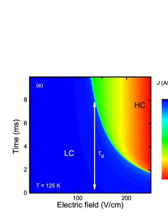
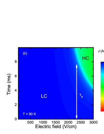
A very distinct jump of occurs when V/cm providing evidence for the transition from a low-conducting to a high-conducting state; this is in excellent accord with the experimental observations. Also the field-dependent behavior of the delay time describes the experimental behavior perfectly. In the simulation the switching occurs at 2000 Vcm-1, while our measurements yield V/cm. The small deviations between simulations and experiments may be due to the neglect of the contact resistance in our two-point measurement [Fig. 2(a)]; it influences and its dependence. Furthermore, we assumed a temperature-independent specific heat and thermal conductivity . Nevertheless, we can conclude that the two-state model perfectly reflects our experimental findings and yields an excellent qualitative and quantitative description.
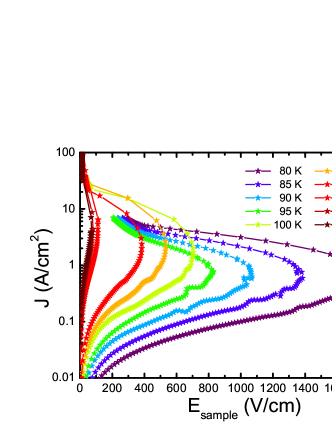
In a next step, the - characteristic is calculated to investigate the nonlinear conductivity and the negative differential resistance (NDR). The results are depicted in Fig. 15 for temperatures between and 130 K. The overall behavior is very similar to the data plotted in Fig. 4 resembling an S-shaped current-voltage curve. All temperatures reveal a linear regime at low fields, they exhibit a turning point which marks the threshold field and current density . All - curves cross over in the NDR regime. Above a certain current density, the field increases again but much steeper than for lower electric fields, indicating that the high-field conduction state is different from the initial state at low fields. Small deviations from the experimental findings can be noted, such as slightly higher current density after the NDR compared to the experiment, or the higher fields for which the curves turn. We attribute these to the unknown contact resistance in the experiment which is in series to the sample and load resistance and affects and , directly. Nevertheless, the detailed agreement of the simulation with the experiment is remarkable.
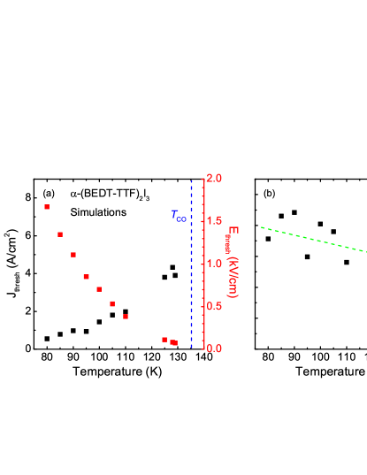
Following our analysis of the experimental data in Sec. II.1, we have extracted the threshold current and the threshold field from the - curves in Fig. 15 and plotted them as a function of temperature in Fig. 16. The results of our simulations resemble more-or-less closely the experimental data displayed in Fig. 5. The observed threshold field was well described by a linear increase as the temperature is reduced below , our simulation, however, rise in a quadratic manner. This may be attributed to the decrease of the occupation number of the conduction band on cooling. Moreover, the increase of at low temperatures can also be attributed by thermal depletion of the conduction band upon cooling.
The calculated current density, on the other hand, decays linearly on cooling, while the experiments seem to flatten at low temperatures. However, the threshold power density increases steeply close to the phase transition and crosses over in regime with a smaller slope, which resembles the development of the energy gap.
We have seen that the two-state model excellently describes the electrically-induced phase transition and explains qualitatively and, impressively, also the quantitative behavior of the experimental values. It does not only support the time-resolved transport measurements, but also explains in detail the observations made in the time-dependent reflectivity study. It confirms that we are dealing with an electronic system linearly coupled to the crystal lattice. Furthermore, we made a precise estimation of the lattice temperature which is different from the electronic system and agrees nicely with estimate sample temperature derived from the comparison of time-dependent reflectivity with the steady-state spectra.
III.3 Field-induced Dirac-like electrons
We have demonstrated that switching into a high-conducting state is caused by excitations of charge carriers into a state with a high mobility. Here, the question arises whether the enhanced mobility is somehow related to the linear band dispersion found in -(BEDT-TTF)2I3. The tilted Dirac cone, i.e. the touching of the bands at the Fermi energy, is only predicted for high pressure. Nevertheless, band structure calculations (Fig. S4) yield that the linear dispersion exists also in the insulating phase.SM ; Pet (b) Furthermore, the temperature-dependence of the resistance under pressure normalized to the room-temperature values exhibit exactly the same slope as the resistance at ambient pressure.Schwenk et al. (1985); Tajima et al. (2006) Since Dirac fermions are made responsible for the conductivity behavior under pressure, we propose, that they also contribute to the metallic state at ambient conditions, excited by a strong electric field. The coexistence of two different types of charge carriers with two orders of magnitude different mobility was previously suggested based on magnetotransportMonteverde et al. (2013) and pressure-dependent optical experimentsBeyer et al. (2016) in -(BEDT-TTF)2I3. We propose that also the electrons excited in the conduction band can act either as normal massive electrons or as massless Dirac-like electrons with very high mobility. This picture provides a consistent explanation of the results presented here.
IV Conclusions
We have reported comprehensive time-resolved investigations of the electrodynamics at the metal-insulator transition in -(BEDT-TTF)2I3. In the charge-ordered state below K, the time- and field-dependent charge transport was measured by applying a voltage pulses along the -direction. We found an electrically-induced resistivity switching from a low-conducting to a high-conducting state, leading to an S-like shape in the - curve. In a regime of negative differential resistance, the electric field across the sample drops drastically above a certain threshold, which increases upon cooling.
Measuring the polarization-dependent infrared reflectivity after a strong electric field was applied, allows us to study the transient optical properties in a wide temperature and field range. From the spectral signature at K , we can identify a field-induced metallic state similar to the high-temperature conducting phase. In contrast, at temperatures well into the insulating state ( K) the reflectivity variations are completely different and cannot be explained by Joule heating. We suggest the creation of an electronically driven high-conducting state in -(BEDT-TTF)2I3. These field-excited charge carriers exhibit an extremely high mobility known from the Dirac-like electrons present under high pressure. Thus we propose that the electrons excited in the conduction band can act either as normal massive electrons or as massless Dirac-like electrons with very high mobility.
This generation of hot charge carriers by the electric field is then simulated with a two-state model. Only based on energy conservation and known material parameters, our numerical simulations can – qualitatively as well as quantitatively – reproduced the experimentally observed properties, such as the temporal behavior of the resistivity as a function of the electric field, the negative differential resistivity, and the different threshold values. By defining an effective electron temperature , we estimate the lattice temperature close to the measured sample temperature. For all parameters analyzed, the quantitative agreement between model and experiment is excellent.
Acknowledgements.
We would like to thank R. Beyer, E. Rose, D. Wu and S. Zapf for useful discussions as well as G. Untereiner for technical support. Funding by the Deutsche Forschungsgemeinschaft (DFG) and Deutscher Akademischer Austauschdienst (DAAD) is acknowledged.References
- Bender et al. (1984a) K. Bender, H. Endres, H.-W. Helberg, I. Hennig, H. Schäfer, H. Keller, and D. Schweitzer, Mol. Cryst. Liq. Cryst. 107, 45 (1984a).
- Dressel et al. (1994) M. Dressel, G. Grüner, J. Pouget, A. Breining, and D. Schweitzer, J. Phys. (Paris) I 4, 579 (1994).
- Kino and Fukuyama (1995) H. Kino and H. Fukuyama, J. Phys. Soc. Jpn. 64, 1877 (1995).
- Kino and Fukuyama (1996) H. Kino and H. Fukuyama, J. Phys. Soc. Jpn. 65, 2158 (1996).
- Seo et al. (2004) H. Seo, C. Hotta, and H. Fukuyama, Chem. Rev. 104, 5005 (2004).
- Takano et al. (2001) Y. Takano, K. Hiraki, H. Yamamoto, T. Nakamura, and T. Takahashi, J. Phys. Chem. Solids 62, 393 (2001).
- Takahashi et al. (2006) T. Takahashi, Y. Nogami, and K. Yakushi, J. Phys. Soc. Jpn. 75, 051008 (2006).
- Moldenhauer et al. (1993) J. Moldenhauer, C. Horn, K. Pokhodnia, D. Schweitzer, I. Heinen, and H. Keller, Synth. Met. 60, 31 (1993).
- Wojciechowski et al. (2003) R. Wojciechowski, K. Yamamoto, K. Yakushi, M. Inokuchi, and A. Kawamoto, Phys. Rev. B 67, 224105 (2003).
- Dressel and Drichko (2004) M. Dressel and N. Drichko, Chem. Rev. 104, 5689 (2004).
- Yue et al. (2010) Y. Yue, K. Yamamoto, M. Uruichi, C. Nakano, K. Yakushi, S. Yamada, T. Hiejima, and A. Kawamoto, Phys. Rev. B 82, 075134 (2010).
- Ivek et al. (2011) T. Ivek, B. Korin-Hamzić, O. Milat, S. Tomić, C. Clauss, N. Drichko, D. Schweitzer, and M. Dressel, Phys. Rev. B 83, 165128 (2011).
- Yakushi (2012) K. Yakushi, Crystals 2, 1291 (2012).
- Kakiuchi et al. (2007) T. Kakiuchi, Y. Wakabayashi, S. Hiroshi, T. Takahashi, and T. Nakamura, J. Phys. Soc. Jpn. 76, 113702 (2007).
- Ivek et al. (2010) T. Ivek, B. Korin-Hamzić, O. Milat, S. Tomić, C. Clauss, N. Drichko, D. Schweitzer, and M. Dressel, Phys. Rev. Lett. 104, 206406 (2010).
- Tomić and Dressel (2015) S. Tomić and M. Dressel, Rep. Progr. Phys. 78, 096501 (2015).
- Lunkenheimer et al. (2015) P. Lunkenheimer, B. Hartmann, M. Lang, J. Müller, D. Schweitzer, S. Krohns, and A. Loidl, Phys. Rev. B 91, 245132 (2015).
- Tajima et al. (2002) N. Tajima, A. Ebina-Tajima, M. Tamura, Y. Nishio, and K. Kajita, J. Phys. Soc. Jpn. 71, 1832 (2002).
- Kobayashi et al. (2004) A. Kobayashi, S. Katayama, K. Noguchi, and Y. Suzumura, J. Phys. Soc. Jpn. 73, 3135 (2004).
- Dressel et al. (1995) M. Dressel, G. Grüner, J. Pouget, A. Breining, and D. Schweitzer, Synth. Met. 70, 929 (1995).
- Ivek et al. (2012) T. Ivek, I. Kovačević, M. Pinterić, B. Korin-Hamzić, S. Tomić, T. Knoblauch, D. Schweitzer, and M. Dressel, Phys. Rev. B 86, 245125 (2012).
- Tajima et al. (2006) N. Tajima, S. Sugawara, M. Tamura, Y. Nishio, and K. Kajita, J. Phys. Soc. Jpn. 75, 051010 (2006).
- Mori (2010) T. Mori, J. Phys. Soc. Jpn. 79, 014703 (2010).
- Tajima et al. (2007) N. Tajima, S. Sugawara, M. Tamura, R. Kato, Y. Nishio, and K. Kajita, Europhys. Lett. (EPL) 80, 47002 (2007).
- Suzumura and Kobayashi (2012) Y. Suzumura and A. Kobayashi, Crystals 2, 266 (2012).
- Kajita et al. (2014) K. Kajita, Y. Nishio, N. Tajima, Y. Suzumura, and A. Kobayashi, J. Phys. Soc. Jpn. 83, 072002 (2014).
- Beyer et al. (2016) R. Beyer, A. Dengl, T. Peterseim, S. Wackerow, T. Ivek, A. V. Pronin, D. Schweitzer, and M. Dressel, Phys. Rev. B 93, 195116 (2016).
- Tajima et al. (2005) N. Tajima, J. Fujisawa, N. Naka, T. Ishihara, R. Kato, Y. Nishio, and K. Kajita, J. Phys. Soc. Jpn. 74, 511 (2005).
- Iwai et al. (2007) S. Iwai, K. Yamamoto, A. Kashiwazaki, F. Hiramatsu, H. Nakaya, Y. Kawakami, K. Yakushi, H. Okamoto, H. Mori, and Y. Nishio, Phys. Rev. Lett. 98, 097402 (2007).
- Kawakami et al. (2010) Y. Kawakami, T. Fukatsu, Y. Sakurai, H. Unno, H. Itoh, S. Iwai, T. Sasaki, K. Yamamoto, K. Yakushi, and K. Yonemitsu, Phys. Rev. Lett. 105, 246402 (2010).
- Iwai (2012) S. Iwai, Crystals 2, 590 (2012).
- Yamamoto et al. (2008) K. Yamamoto, S. Iwai, S. Boyko, A. Kashiwazaki, F. Hiramatsu, C. Okabe, N. Nishi, and K. Yakushi, J. Phys. Soc. Jpn. 77, 074709 (2008).
- Yamamoto et al. (2010) K. Yamamoto, A. Kowalska, and K. Yakushi, Appl. Phys. Lett. 96, 122901 (2010).
- Yamamoto et al. (2012) K. Yamamoto, A. A. Kowalska, and K. Yakushi, phys. stat. sol. (c) 9, 1189 (2012).
- Naito (2010) T. Naito, Molecular Electronic and Related Materials-Control and Probe with Light (Transworld Research Network, Kerala, India, 2010).
- Iimori and Ohta (2014) T. Iimori and N. Ohta, J. Phys. Chem. C 118, 7251 (2014).
- Nakaya et al. (2008) H. Nakaya, F. Hiramatsu, Y. Kawakami, S. Iwai, K. Yamamoto, and K. Yakushi, J. Luminescence 128, 1065 (2008).
- Iimori et al. (2009) T. Iimori, T. Naito, and N. Ohta, J. Phys. Chem. C 113, 4654 (2009).
- Iimori et al. (2007a) T. Iimori, T. Naito, and N. Ohta, Chem. Lett. 36, 536 (2007a).
- Iimori et al. (2007b) T. Iimori, T. Naito, and N. Ohta, J. Am. Chem. Soc. 129, 3486+ (2007b).
- Tamura et al. (2010) K. Tamura, T. Ozawa, Y. Bando, T. Kawamoto, and T. Mori, J. Appl. Phys. 107, 103716 (2010).
- Katayama et al. (2006) S. Katayama, A. Kobayashi, and Y. Suzumura, J. Phys. Soc. Jpn. 75, 054705 (2006).
- Alemany et al. (2012) P. Alemany, J.-P. Pouget, and E. Canadell, Phys. Rev. B 85, 195118 (2012).
- Bender et al. (1984b) K. Bender, I. Hennig, D. Schweitzer, K. Dietz, H. Endres, and H. Keller, Mol. Cryst. Liq. Cryst. 108, 359 (1984b).
- (45) See the Supplemental Matierials for details of the experimental setup, a description of the transport measurements, and estimates of the Joule heating, describtion of the bandstructure and two-state model.
- Itose et al. (2013) F. Itose, T. Kawamoto, and T. Mori, J. Appl. Phys. 113, 213702 (2013).
- Ozawa et al. (2009) T. Ozawa, K. Tamura, Y. Bando, T. Kawamoto, T. Mori, and I. Terasaki, Phys. Rev. B 80, 155106 (2009).
- Grüner (1988) G. Grüner, Rev. Mod. Phys. 60, 1129 (1988).
- Maki (1986) K. Maki, Phys. Rev. B 33, 2852 (1986).
- Dressel and Grüner (2002) M. Dressel and G. Grüner, Electrodynamics of Solids (Cambridge University Press, Cambridge, 2002).
- Clauss et al. (2010) C. Clauss, N. Drichko, D. Schweitzer, and M. Dressel, Physica B 405, S144 (2010).
- Pet (a) T. Peterseim and M, Dressel, arXiv:1604.00977.
- Mori et al. (2009) T. Mori, T. Ozawa, Y. Bando, T. Kawamoto, S. Niizeki, H. Mori, and I. Terasaki, Phys. Rev. B 79, 115108 (2009).
- Zimmers et al. (2013) A. Zimmers, L. Aigouy, M. Mortier, A. Sharoni, S. Wang, K. G. West, J. G. Ramirez, and I. K. Schuller, Phys. Rev. Lett. 110, 056601 (2013).
- Kroll (1974) D. M. Kroll, Phys. Rev. B 9, 1669 (1974).
- Sze and Ng (2007) S. M. Sze and K. K. Ng, Physics of Semiconductor Devices (Wiley-Interscience, Hoboken, N.J, 2007), 3rd ed.
- Yu and Cardona (2010) P. Y. Yu and M. Cardona, Fundamentals of Semiconductors: Physics and Materials Properties (Springer, Berlin, 2010), 4th ed.
- (58) For our calculations we set the lattice temperature equal to the environment temperature . The last term corresponds to the experimental situation described by Fig. 11(b) and (d): the reflectivity does not change and correspondingly the sample has a constant temperature. We have assumed a linear Newton cooling.
- Fortune et al. (1991) N. A. Fortune, K. Murata, M. Ishibashi, M. Tokumoto, N. Kinoshita, and H. Anzai, Solid State Commun. 79, 265 (1991).
- Pet (b) T. Peterseim and M, Dressel, arXiv:1603.07505.
- Schwenk et al. (1985) H. Schwenk, F. Gross, C.-P. Heidmann, K. Andres, D. Schweitzer, and H. Keller, Mol. Cryst. Liq. Cryst. 119, 329 (1985).
- Monteverde et al. (2013) M. Monteverde, M. O. Goerbig, P. Auban-Senzier, F. Navarin, H. Henck, C. R. Pasquier, C. Mézière, and P. Batail, Phys. Rev. B 87, 245110 (2013).