High-field electron transport in bulk ZnO
Abstract
Current-voltage dependence is measured in (Ga,Sb)-doped ZnO up to 150 kV/cm electric fields. A channel temperature is controlled by applying relatively short (few ns) voltage pulses to two-terminal samples. The dependence of electron drift velocity on electron density ranging from 1.421017 cm-3 to 1.31020 cm-3 at a given electric field is deduced after estimation of the sample contact resistance and the Hall electron mobility. Manifestation of the highest electron drift velocity up to 1.5107 cm/s is estimated for electron density of 1.421017 cm-3 and is in agreement with Monte Carlo simulation when hot-phonon lifetime is below 1 ps. A local drift velocity maximum is observed at 1.11019 cm-3 and is in agreement with ultra-fast hot phonon decay.
1 Introduction
Semiconducting zinc oxide (ZnO) seems to be a potential material for optical and electronic applications [1]. It has a relatively wide bandgap (3.37 eV) similar to GaN and is transparent. Expected high structural quality promises efficient operation of high power ZnO field-effect transistors at centimeter and millimeter-wave frequencies [2]. The epitaxial technology is less expensive, albeit relatively not as well developed. The electron mobility is mainly determined by scattering on extended defects and ionized impurities in heavily doped layers, while polar scattering by longitudinal optical phonons (LO phonons) is important at low and moderate electron densities [3, 4]. The electron mobility is not as high than in GaN but the value slightly above 400 cm(Vs) is achieved in epitaxial layers at room temperature and low residual impurity densities [5].
The supplied electric power is dissipated mainly through electron coupling with LO phonons, while the defect and ionized impurity scattering is elastic and acoustic phonon scattering is quasi-elastic. Because the high-field electron transport is accompanied with intense LO-phonon emission by hot electrons, the emitted non-equilibrium LO phonons accumulate, and the associated phenomena are often referred to as hot-phonon effects. In general, hot phonons play an important role in devices operated at high electric fields such as microwave and high power field-effect transistors because of pivotal role they play in heat dissipation and device reliability [6]. The fastest decay of hot phonons takes place in the vicinity of plasmon -LO-phonon resonance [7]. Essentially, the plasmon-assisted ultrafast decay of hot phonons accompanied with very short LO-phonon lifetimes causes fast electron energy relaxation [8], high electron drift velocity[9, 10] and the best operation of the device.
Accumulation of non-equilibrium (hot) longitudinal optical (LO) phonons reduces the electron drift velocity but causes a weak effect if their decay is fast [11, 12, 9]. Initial studies of high-field electron transport measurements in epitaxial ZnO structures was reported in Ref.[13]. The dependence of electron drift velocity on applied electric field was deduced at room temperature for nominally undoped MBE grown ZnO up to 100 kV/cm [14]. Although short enough voltages pulses (300 ns) were used to heat the electrons, the self-heating effect due to current caused relatively low drift velocity values (7.6 cm/s). No experimental studies of the velocity dependence on the electron density was reported.
In this work the current–voltage dependence at different electron densities was measured for (Ga,Sb) doped ZnO films at high electric fields. Nearly-equilibrium acoustic phonon temperature was ensured by the semi-automated few-nanosecond-pulsed voltage technique. The electron drift velocities were deduced under assumption of uniform electric field and constant electron density. Monte Carlo simulation data obtained by taking hot phonons into account were used to interpret experimental results.
2 Samples
The ZnO films were grown on a-plane sapphire substrates by plasma-enhanced molecular beam epitaxy (PMBE). Plasma power of 400 W was used for depositing of the films. The growth of the ZnO films was monitored by in situ reflection high energy electron diffraction. A 5-nm-thick low-temperature ZnO buffer layer was deposited at C for enhanced nucleation and 10 annealed at C prior to the growth of doped ZnO layer. The layer thickness was 150- 350 nm. Structural properties and surface morphology were studied by X-ray diffraction, transmission electron microscopy, and atomic force microscopy. The transmission line model (TLM) patterns were processed with evaporated stacks of Ti/Au (25 nm/30 nm ) acting as Ohmic contacts. The channel width was 250-300 m and the length (inter-electrode distance) was 1.7, 2.9, 3.9, 5.8, 6.1, 6.9, 9.2, 9.9, 14.8, 16,8, 17.3 m. The Hall effect measurements were performed in the van der Pauw configuration with soldered indium contacts. The Hall mobility values measured for the investigated channels ranged from 110/(Vs) to 23/(Vs). The 3DEG density assessed from Hall measurements ranged from 1.421017cm-3 to 5.71020cm-3. The electron density, mobility values and the channel thickness are listed in Table 1.
| Wafer | dopant | |||
|---|---|---|---|---|
| cm-3 | /V s | nm | ||
| #567 | Ga | 106 | 330-340 | |
| #570 | Ga | 73 | 350 | |
| #639 | Ga | 23 | 300 | |
| #753 | Ga | 57 | 200 | |
| #751 | Ga | 66 | 200 | |
| #487 | Sb | 110 | 170 | |
| #661 | Ga | 25-30 | 150 | |
| #658 | Ga | 48 | 350 | |
| #592 | Ga | 40 | 380 |
The contact resistance was estimated at low electric fields from the dependence of the sample resistance on the channel length.
3 Methods
The electron transport measurements at high electric fields were carried out on two-electrode samples taken from the TLM structures. The sample was placed into a gap of a micro-strip line. The measurement procedure and the determination of current–voltage dependence is described in Refs.[15, 16]. The employment of nanosecond pulses enabled us to minimize the complications caused by channel self-heating due to current. The electron drift velocity was estimated under assumptions that the electric field was uniform and 2DEG density was independent on the electric field: = ), where is an elementary charge.
The channels suffered soft damage at high electric fields. The damage was characterized by the change of the zero-field channel resistance measured before and after the high-field experiment. We present the results up to a damage level not exceeding 5 %. The soft damage turned into the channel breakdown at higher fields.
Ensemble Monte Carlo simulation was carried out for bulk wurtzite ZnO crystals at 300 K lattice temperature. The electron motion and scattering in the one-valley spherical parabolic conduction band was considered. In the range of electric fields under investigation, electron scattering into the upper valleys was expected to be unimportant and the inter-valley transfer was neglected [17]. The scattering mechanisms included in the simulation were: acoustic phonon scattering, LO phonon scattering, and ionized impurity scattering.
The hot-phonon effect was included in the Monte Carlo model for ZnO in a manner described previously [18]. The LO-phonon distribution was updated after each event of LO-phonon emission and absorption, and after decay of the excess LO phonons. The decay into modes of the unperturbed thermal bath was treated. The time-dependent LO-phonon distribution was calculated under the assumption of dispersion-less LO phonons. The decay of excess LO phonons into other modes of the thermal bath was treated in the LO-phonon lifetime approximation, the Ridley model was used [19]. The results of the Monte Carlo simulations are used to calculate the mean electron energy, electron energy autocorrelation function and electron drift velocity. The simulations were carried out at a fixed background temperature of acoustic phonons representing the thermal bath for the subsystem of hot electrons and hot phonons. As mentioned, the channel background temperature differs from the hot-electron temperature and the remote heat sink temperature.
4 Results and discussion
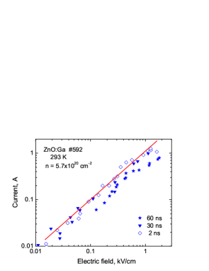
Pulsed technique is used to investigate dependence of current on voltage. Hot electrons and hot phonons are the main causes for non-ohmic behaviour at high electric fields when the pulses of voltage are sufficiently short. Because of strong electron-LO-phonon coupling in ZnO, emission of LO phonons by hot electrons is the preferred route for dissipation of the heat gained by the mobile electrons from the applied electric field. The dissipation of the electronic heat is partly compensated by re-absorption of the emitted LO phonons. Thus the heat is shared by the hot electrons and the hot phonons before it is converted into the heat modes able to propagate across the electrically non-conductive layers towards the remote heat sink. The bottleneck forms if the hot-phonon conversion is slow and the associated hot-phonon lifetime is long. The dependence of current on the pulse duration is associated with increase in the background temperature. Nanosecond pulses of voltage are used in order to minimize the thermal walkout as illustrated for high electron density sample #592 (Figure 1, see also [20]).
The experimental data for sample #567 are illustrated in Figure 2 (closed squares, triangles).
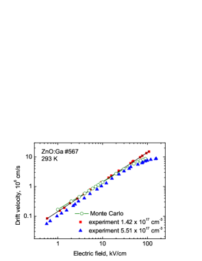
The highest electric field of 150 kV/cm is reached for electron density of 5.511017 cm-3 (blue triangles). The Ohm law (black line) approximately holds at electric fields up to 100 kV/cm at the electron density of 1.421017 cm-3 (red squares). The drift velocity is 1.5107 cm/s at 104 kV/cm. This value for the drift velocity exceeds the recently published experimental result of 7.6106 cm/s at around 100 kV/cm at the electron density of 2.41016 cm-3 measured in nominally undoped ZnO structures grown by MBE [13, 14].
Sample #487 with a higher electron density of 4.61019 cm-3 demonstrates lower values for the drift velocity (Fig. 3, red squares). The velocity is close to 3105 cm/s at 6 kV/cm for sample #487 (Fig. 3, squares) in contrast to a higher value of 8.5105 cm/s at the same electric field for sample #567 (Fig. 2, squares). The application of 2 ns voltage pulses enabled us to measure the drift velocity at electric fields up to 150 kV/cm (Fig. 2, triangles).
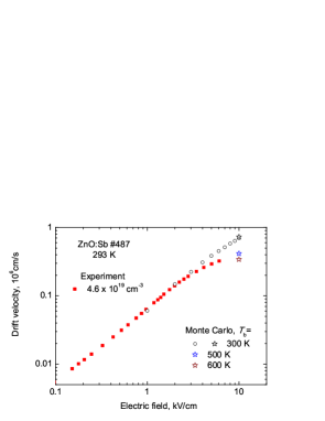
The experimental electron drift velocity increases linearly with the applied electric field at electron density of 1.421017 cm-3 (Fig. 2). This behavior fortuitously indicates a weak impact of the hot phonons on the electron transport. On the other hand, an essential deviation from the Ohm law is observed at electron density of 4.61019 cm-3 (Fig. 3). The experimental results are compared with those of Monte Carlo simulations.
The impurity scattering is taken into account in order to fit the experimental data at low electric field. The density of impurities is artificially increased over the density of electrons-high impurity/electron density ratio is used, the compensation ratio is from 10 to 13. This is an important argument for strong elastic electron scattering in the investigated samples. Since we aim at investigation of hot-electron energy relaxation, we feel safe to mimic scattering on impurities, defects and lattice imperfections by ionized impurity scattering: the scattering on both charged and neutral lattice imperfections is usually assumed to be elastic. The results of Monte Carlo simulation are illustrated in Figures 2 and 3 under a realistic assumption that the hot-phonon lifetime is equals 1 ps (open circles and stars). The comparison with the experimental results suggests that the lifetime is below 1 ps for sample #567 (squares).
The short voltage pulses help to reduce the thermal walkout effect unless the electron density is high and the electric field is strong. Figure 3 presents the results at high electron density (4.61019 cm-3) in the electric field range below 6 kV/cm. The thermal walkout turns into the electrothermal breakdown at stronger electric fields even when the voltage pulses of 2 ns are applied. Stars in Fig. 3 illustrate the simulated hot-electron drift velocity at different background temperatures. The drift velocity decreases as the background temperature increases. Therefore, the experimental deviation from the Ohm law cannot be interpreted in terms hot-electron energy relaxation. An interpretation in terms of elevated background temperature seems quite probable (cf. closed square and wine star in Figure 3). The alternative interpretation of the experimental data in terms of hot-phonon lifetime requires unrealistically long lifetimes-significantly longer than 1 ps-if the thermal walkout is ignored.
The enhanced resonance decay of hot phonons has a direct consequence on various phenomena where the excess occupancy of hot-phonon modes plays an important role [7, 10, 6, 21]. In particular, the electron scattering by the non-equilibrium excess (hot) phonons is weaker if the occupancy of the involved hot-phonon modes is lower. This can be demonstrated by measuring the hot-electron drift velocity in various samples at the chosen value of applied electric field.
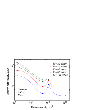
Typically, the effect is masked by the Joule effect: the increase in background temperature causes a stronger scattering of electron by acoustic phonons. The Joule effect is important at high electric field in channels with high electron density. Application of short pulses of voltage allows one to reduce the thermal walkout effect dramatically. Let us plot the density dependence of the drift velocity (Fig. 4). Typically, the drift velocity decreases if the doping increases. This happens in the electron density range from 11017 cm-3 to 51018 cm-3 for doped ZnO (Fig. 4, symbols). The velocity stops decreasing at around 51018 cm-3, and the local maximum forms at higher densities at intermediate electric fields in the range from 20 kV/cm to 60 kV/cm (triangles, squares, stars). The thermal runaway makes it impossible to resolve the maximum at electric fields of 80 kV/cm and 100 kV/cm (diamonds, circles). The maximum is located at above 1019 cm-3. Its position (Fig. 4) correlates with that of the resonance decay of hot phonons [8]. Thus, the observed fast decay of hot phonons supports high values of hot-electron drift velocity unless the thermal runaway comes into play.
5 Conclusions
The nanosecond pulsed measurements yielded hot-electron drift velocity in agreement with those of the Monte Carlo simulation when the density of the ionized impurities is allowed to exceed that of the electrons by 10- 13 times in bulk ZnO. The Ohm law approximately held in the electric field range up to 100 kV/cm at an electron density of 1.421017 cm-3 but the range shrank at higher electron densities. The LO-phonon–plasmon resonance supported increase in the electron drift velocity is resolved at (1019 cm-3). The non-ohmic behavior at higher densities (1019 cm-3) is caused by increase in the background temperature represented by acoustic phonons. A drift velocity of 1.5107 cm/s was measured at 104 kV/cm field. A lot of effort still to be done to design ZnO-based field-effect transistors with improved electron transport along a channel.
Acknowledgement
This research is funded by the Research Council of Lithuania (grant No. APP-5/2016).
References
- [1] Morkoç H 2009, Zinc Oxide: Fundamentals, Materials and Device Technology (Weinheim: Wiley-VCH)
- [2] Liu H, Avrutin V, Izyumskaya N, Özgür Ü, Morkoç H 2010 Supperlattices Microstruct. 48 458
- [3] Look D C, Leedy K D, Tomich D H, and Bayraktaroglu B 2006 Appl. Phys. Lett. 96 062102
- [4] Liu Y, Avrutin V, Izyumskaya N, Özgür Ü, Yankovich A B, Kvit A V, Voyles P M, and Morkoç H 2012 J. Appl. Phys 111 103713
- [5] Tsukazaki A, Ohtomo A, and Kawasaki M 2006 Appl. Phys. Lett. 88 152106
- [6] Matulionis A, Liberis J, Šermukšnis E, Ardaravičius L, Šimukovič A, Kayis C, Zhu C Y, Ferreyra R, Avrutin V, Özgür Ü, Morkoç H 2012 Microelectron. Reliab. 52 2149
- [7] Matulionis A, Liberis J, Matulionienė I, Ramonas M, and 2010 Proc. IEEE 98 1118
- [8] Šermukšnis E, Liberis J, Ramonas M, Matulionis A, Toporkov M, Liu H Y, Avrutin V, Özgür Ü, and Morkoç H 2015 J. Appl. Phys. 117 065704
- [9] Liberis J, Ramonas M, Šermukšnis E, Sakalas P, Szabo N, Schuster M, Wachowiak A, and Matulionis A 2014 Semicond. Sci. Technol. 29 045018
- [10] Ardaravičius L, Liberis J, Kiprijanovič O, Matulionis A, Wu M, and Morkoç H 2011 Phys. Status Solidi RRL 5 65
- [11] Khurgin J, Ding Y J, and Jena D 2007 Appl. Phys. Lett. 91 252104
- [12] Dyson A and Ridley B K 2010 J. Appl. Phys. 108 104504
- [13] Sasa S, Hayafuji T, Kawasaki M, Nakashima A, Koike K, Yano M, and Inoue M 2008 Phys. Status Solidi C 5 115
- [14] Sasa S, Maitani T, Furuya Y, Amano T, Koike K, Yano M, and Inoue M 2011 Phys. Status A 208 449
- [15] Ardaravičius L, Ramonas M, Liberis J, Kiprijanovič O, Matulionis A, Xie J, Wu M, Leach J H, and Morkoç H 2009 J. Appl. Phys. 106 073708
- [16] Ardaravičius L, Kiprijanovič O, Liberis J, Matulionis A, Šermukšnis E, Ferreyra R A, Avrutin V, Özgür Ü, and Morkoç H 2015 Semicond. Sci. Technol. 30 105016
- [17] Furno E, Bertazzi F, Goano M, Ghione G, and Bellotti E 2008 Solid-State Electron. 52 1796
- [18] Ramonas M, Matulionis A, Liberis J, Eastman L F, Chen X, and Sun Y J 2005 Phys. Rev. B 71 075324
- [19] Ridley B K 1996 J. Phys.: Condens. Matter 8 L511
- [20] Ardaravičius L, Matulionis A, Liberis J, Kiprijanovic O., Ramonas M, Eastman L F, Shealy J. R, and Vertiatchikh A 2003 Appl. Phys. Lett. 83 4038
- [21] Matulionis A 2013 Semicond. Sci. Technol. 28 074007