Atomic defect states in monolayers of MoS2 and WS2
Abstract
The influence of atomic vacancy defects at different concentrations on electronic properties of MoS2 and WS2 monolayers is studied by means of Slater-Koster tight-binding model with non-orthogonal orbitals and including the spin-orbit coupling. The presence of vacancy defects induces localized states in the bandgap of pristine MoS2 and WS2, which have potential to modify the electronic structure of the systems, depending on the type and concentration of the defects. It is shown that although the contribution of metal (Mo or W) orbitals is dominant in the formation of midgap states, the sulphur and orbitals have also considerable contribution in the localized states, when metal defects are introduced. Our results suggest that Mo and W defects can turn the monolayers into p-type semiconductors, while the sulphur defects make the system a n-type semiconductor, in agreement with ab initio results and experimental observations.
pacs:
71.55.Ak, 71.20.Mq, 31.15.aqI Introduction
Layered transition metal dichalcogenides (LTMDs) have attracted intensive attentions in recent years due to their intrinsic non-zero bandgap, which gives them a superior advantage over graphene for use in nanoelectronic and optoelectronic applications such as field-effect transistors and electroluminescent devices Wang ; Ataca . This class of layered materials with chemical composition of MX2, where M and X correspond to the transition metal and the chalcogen elements, respectively, crystallizes in a hexagonal structure like graphene in which the M-atom layer is covalently bonded and sandwiched between the two X-atom layers. Among LTMD materials, MoS2 and WS2 monolayers with a direct bandgap configuration have been extensively investigated because of many intriguing physical and chemical properties Radisavljevic ; Braga ; ZhenZhou . These compounds can be synthesized through various methods, such as mechanical exfoliation Novoselov , chemical vapor deposition Zhang , and intercalation techniques Eda . In addition, they have quite similar lattice constants which also enable the synthesis of MoS2-WS2 heterostructures with minimum interfacial defects Kang ; Kosmider ; Chen ; Yoo ; Gong .
Point defects such as atomic vacancies may cause a large variation in the electronic and optical properties of LTMDs. Vacancy defects, which can be created by thermal annealing and particles Tongay or electron beam irradiation Zhou , form localized trap states in the bandgap region, leading to light emission at energies lower than the interband optical transition energy Tongay . On the other hand, the observed charge mobility in single-layer MoS2 is surprisingly low compared to bulk sample Novoselov ; Radisavljevic , indicating that the charge carrier scattering by structural defects, such as vacancies and grain boundaries, may be a primary source for such a low mobility Tongay ; Enyashin ; Asl . Hong et al. Hong have studied point defects and their concentrations for several samples of MoS2 by means of different preparation methods. They found that the dominant type of point defects in each sample is strongly dependent on the chosen sample preparation method. Nevertheless, the sulphur vacancy is the predominant point defect compared to Mo vacancy, regardless of the type of preparation method. Hong
The effects of point defects on the electronic structure of LTMDs have also been theoretically studied by several groups using first principles calculations Enyashin ; Asl ; Ataca2 ; Ma ; Komsa ; Wei ; Liu ; Zhou2 ; BHuang and 6-band tight-binding (TB) model Yuan . Although, ab initio methods based on density functional theory (DFT) can achieve a good degree of accuracy to describe the electronic structure of pristine LTMD materials, they are limited in their application by the presence of defects in the samples. For instance, simulation of vacancy-doped MoS2 and WS2 monolayers with a random distribution of vacancies requires a very large supercell in the calculations which is computationally expensive for DFT methods. With TB approach which is a simpler and less computationally demanding method, however, it is possible to deal with such large systems. The use of large supercells within TB model makes it also possible to eliminate the vacancy-vacancy interactions from the calculations.
After the two-band model describing the conduction and valence bands around the two valleys (K and K′ points) in the hexagonal Brillouin zone of LTMD Xiao , several TB models in various approximations have been proposed to reproduce the first-principles band structure of pristine LTMD Rostami ; Zahid ; Cappelluti ; Roldan ; Liu . Among them, the TB model of Zahid et al. Zahid , including nonorthogonal orbitals of M and X atoms and spin-orbit coupling, is able to accurately reproduce the first-principles bands for a wide range of energies in the Brillouin zone. The model considers nearest-neighbor Slater-Koster hopping matrix elements of M-M, M-X, and X-X, which can be applied to monolayers, bilayers and bulk MX2 Zahid .
In this work, based on the parameterized TB model of Zahid et al. Zahid , we explore the influence of vacancy defects on the electric properties of MoS2 and WS2 monolayers to see how the missing atoms at different concentrations evolve the intrinsic bandgap and electronic states of the monolayers. Since the model presents an accurate description for the band structure of LTMDs, the application of this model to defective MoS2 and WS2 provides a more realistic understanding of the electronic states contributing to the process of vacancy formation and the accurate location of defect states within the bandgap. Moreover, the optimized geometries of the monolayers obtained by ab initio calculations have demonstrated that atomic vacancies do not cause a considerable geometry deformation and the neighboring atoms around the vacancies do not show any visible displacement Wei ; Ataca . Therefore, the defect-induced deformation is ignored. We show that the vacancy defects mainly induce localized states within the bandgap of pristine MoS2 and WS2, leading to a shift of the Fermi level toward valance or conduction band, depending on the type of vacancy. The rest of this paper is as follows. In section II we introduce our model and formalism for calculation of band structure and electronic states of the defective monolayers. Numerical results and discussion for electronic properties of MoS2 and WS2 with different types and concentrations of vacancy defects are presented in Sec. III. A brief conclusion is given in Sec. IV.
II Model and formalism
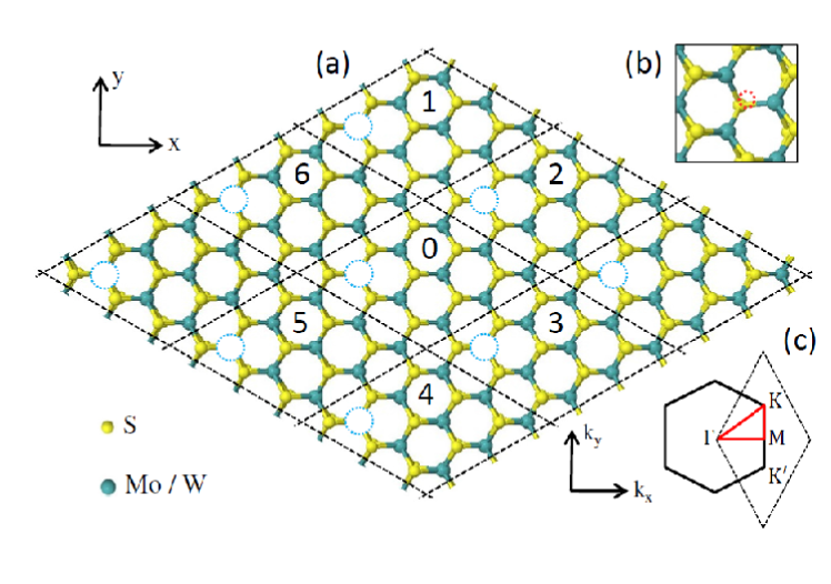
The band structure of defective MoS2 and WS2 is carried out within the non-orthogonal Slater-Koster scheme Slater . From DFT calculations Zahid , we know that the bands of both structures are made up of the , , and valence orbitals of Mo, W, and S atoms. Therefore, a basis set consisting of , , , , , , , , orbitals is used as a starting point for constructing the TB Hamiltonian. This means that for a monolayer MX2 with one M atom and two X atoms per unit cell, we should consider a 27-band TB spinless model. Moreover, a Bloch sum is taken into account for each atomic orbital on each atomic site in the unit cell due to the periodicity of the monolayer. On the other hand, in order to model a defective MX2 monolayer with different vacancy concentrations the system is partitioned into supercells each containing unit cells where is an integer number. Figs. 1(a) and 1(b) show such a monolayer with 33 supercells each containing a single vacancy defect. Since all the valence orbitals of the atoms belonging to the supercell are included in the atomic orbitals basis set, the number of bands increases with the size of the supercell. The total Hamiltonian of MX2 monolayer can be written as
| (1) |
where represents the Slater-Koster tight-binding Hamiltonian for non-orthogonal orbitals, is the identity matrix, and is an atomiclike spin-orbit coupling. has the same form for both spin-up and spin-down states and can be expressed in the real space as
| (2) |
where is the creation operator for an electron in an atomic valence orbital at -th atom, , with on-site energy . The hopping parameters, , between atomic orbitals and are real Slater-Koster integrals that depend for each orbital pair on the directional cosines of the vector connecting nearest neighbors and on the Slater-Koster TB parameters , , , , , , , , , , , , , and for MoS2 Zahid and WS2 Private . These parameters are related to hopping processes between nearest-neighbor Mo-S (W-S), between the nearest-neighbor in-plane Mo-Mo (W-W), and between the nearest-neighbor in-plane and out-of-plane S-S atoms in MoS2 (WS2) monolayer. The hopping terms between next nearest neighbors are ignored in this model.
The intra-atomic spin-orbit interaction acting on both the transition metal and the chalcogen atoms is incorporated in the Hamiltonian via the second term in Eq. (1) which is written as Roldan ,
| (3) |
where are the Pauli spin matrices, is the atomic angular momentum operator, and is the intra-atomic spin-orbit coupling constant which depends on the type of atom . In the presence of such a spin-orbit coupling, inversion symmetry breaking in the LTMD materials lifts the spin degeneracy of the energy bands, leading to a strong spin-splitting in the valence-band maximum (VBM) Xiao .
Within the non-orthogonal scheme, the orbital overlap obtained from Slater-Koster parameters, can be non-zero. Therefore, the band structure of the system is calculated by solving the generalized eigenvalue problem:
| (4) |
where denotes the eigenvector of the band and is an allowed wave vector in the two-dimensional Brillouin zone, shown in Fig. 1(c). Note that the size of Hamiltonian and overlap, , matrices (including spin), which is the same as the size of and in the real space, is equal to , where is the number of basis orbitals per supercell and 2 is for spin. In the absence of vacancy defects, the size of these matrices, including the spin-orbit interaction for a monolayer with supercells, is . To introduce a single vacancy defect, we remove one atom from the supercell while the symmetry of the lattice remains intact Papa . This reduces the number of atomic orbitals in each supercell and hence the size of matrices.
The Hamiltonian and overlap matrices in the discrete version of Bloch’s theorem Datta can be written as
| (5) |
| (6) |
where is the supercell index and the summation runs over all neighboring supercells including the reference supercell, as shown by in Fig. 1(a). Because of the periodicity of the lattice in Fig. 1(a), the result is independent of the reference unit cell that we choose. The Green’s function of MX2 monolayer is defined by where is a positive infinitesimal. Accordingly, the local density of states (DOS), , for an electron with spin in an atomic orbital at site in the supercell can be obtained directly from the Green’s function of the MX2 monolayer through Lopez
| (7) |
Therefore, the partial DOS of an atomic orbital in the unit cell is simply given as .
III results and discussion
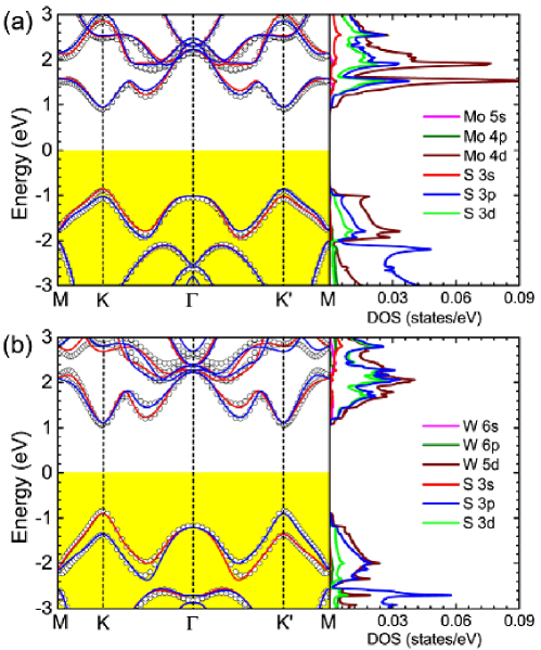
We now use the method described above to study the influence of single vacancy defects on electronic properties of MoS2 and WS2 monolayers. First, we discuss the TB band structure and partial DOS of the pristine monolayers in the presence of spin-orbit interaction and their consistency with DFT calculations. It should be mentioned that for more quantitative agreement between our TB results and fully-relativistic ab-initio DFT calculations Xiao , we include the spin-orbit coupling between Mo orbitals, instead of orbitals and only between W orbitals, instead of and orbitals used in Ref. Zahid, . The fitted spin-orbit parameters, the valence-band spin-splitting values, and the band gaps obtained in this way are presented in Table I. The bandgap values of 1.80 eV for MoS2 and 1.98 eV for WS2 and the valence band spin-orbit splittings, obtained using this method, are in good agreement with DFT Zahid ; Feng ; Kang and experimental values Mak . Note that the single-layer WS2 has a larger bandgap because the crystal field splitting of the metal states, which is larger in W compared to Mo, is responsible for a large part of the bandgap Mattheiss . In addition, the valence band spin-splitting in WS2 is almost three times larger than that in MoS2, which makes the observation of valley and spin Hall effect easier in WS2 Xiao .
| MoS2 | 0.130 | 0.057 | 0.154 | 1.80 |
|---|---|---|---|---|
| WS2 | 0.422 | 0.057 | 0.449 | 1.98 |
Figs. 2(a) and 2(b) show the electronic structure with the projection of spin operator and the corresponding partial DOS of MoS2 and WS2 monolayers, respectively. We see that both monolayers have a direct bandgap at the two inequivalent corners K and K′ of the Brillouin zone (Fig. 1(c)). The spin splittings in the band structures along -K-M and -K′-M lines are opposite which lead to valley-selective optical absorption and may cause optically induced valley and spin Hall effects Xiao . Comparing the band structures with that given in Refs. Feng, , Wickramaratne, , and Gibertini, clearly shows the quantitative agreement between TB and DFT results (see hollow circles in Fig. 2). From the partial DOS of pristine monolayers one can see the contribution of each type of atomic orbitals to the formation of energy bands. The conduction-band minimum (CBM) and the VBM of MoS2 (WS2) are mostly dominated by Mo (W) orbitals and S orbitals, in agreement with DFT Feng . Moreover, the inclusion of S orbitals in our model leads to a nonzero contribution to the electronic states which is comparable to S orbitals in the conduction band.
To study atomic vacancy defects, the monolayer is partitioned into supercells and one atom from each supercell is removed without any change in the symmetry of the lattice (see Fig. 1(a)). We have examined several supercell sizes (33, 44 and 55) to reveal the strength of vacancy-vacancy interaction on the localized midgap states. Note that in the supercell calculations, as the supercell grows in size, the corresponding Brillouin zone in the -space shrinks and the bands in the original (normal) Brillouin zone get folded into the supercell Brillouin zone. In other words, if the supercell is times larger than the normal cell, the Brilouin zone of the supercell will be times smaller and will contain times more bands.
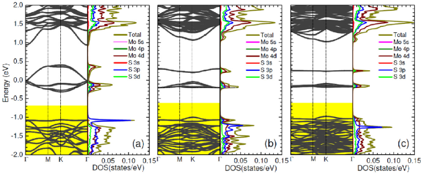
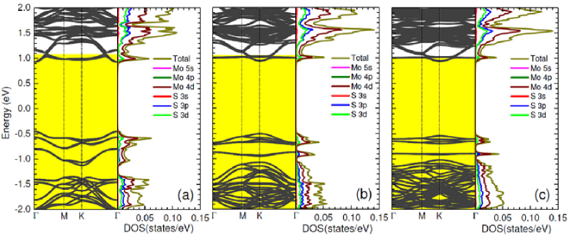
Now, let us consider metal vacancies at different concentrations in MoS2 and WS2 monolayers. In Fig. 3, we show the band structure and the corresponding partial DOS of MoS2 when a Mo vacancy is introduced. Since each supercell contains only one atomic vacancy defect, the size of supercell manifests itself as a measure of defect concentration. Accordingly, the Mo defect concentration per supercell in Fig. 3(a)-3(c) is , , and , respectively. The defect concentrations represent the ratio of number of vacancies to the number of atomic sites per supercell which correspond to vacancy densities of , , and cm-2, respectively. We see that at high vacancy concentration, i.e., , the defect states form a band in the middle of the gap, whose width is 0.73 eV (see Fig. 3(a)). The midgap band creates defect states with three peaks in the DOS spectrum arising from neighboring Mo orbitals and S and orbitals around the defect. In addition, the vacancy defect induces a sharp peak at the top of the valence band (Fig. 3(a)), corresponding to S orbitals, which shifts toward lower energies as the concentration decreases. The midgap band splits into two bands centered around Fermi level of pristine MoS2 as shown in Fig. 3(b). These bands become more localized at concentration (Fig. 3(c)) indicating that gap states generated by Mo vacancies are mainly localized around atomic defects, in agreement with Ref. Yuan, . It is important to point out that the position of Fermi energy is determined by counting the number of electrons that the atoms in the supercell provide. These electrons fill up the lowest energy bands and hence, the Fermi level lies between the highest occupied band and the lowest unoccupied band.
We now consider the effect of metal vacancies on electronic structure of WS2 monolayer at different defect concentrations, as shown in Figs. 4(a)-4(c). The band structure of Fig. 4(a) shows two midgap bands in their close proximity, located below the Fermi energy of the pristine monolayer. These bands form a single narrow band with three peaks in the partial DOS, associated with localized states around the defects as the concentration decreases (see Fig. 4(b) and 4(c)). We see that the midgap states originate mainly from W orbitals and S and orbitals, indicating that the contribution of S orbitals could be considerable in the electronic structure of LTMD when metal vacancies are introduced in the system. Moreover, contrary to the electronic structure of defective MoS2 with Mo vacancies, the induced sharp peak at the top of the valence band, corresponding to the S orbitals, is not shifted down in energy as the distance between point defects in WS2 monolayer increases. This reveals a strong hybridization between sulphur atoms, and hence, localization of S states around W defects.
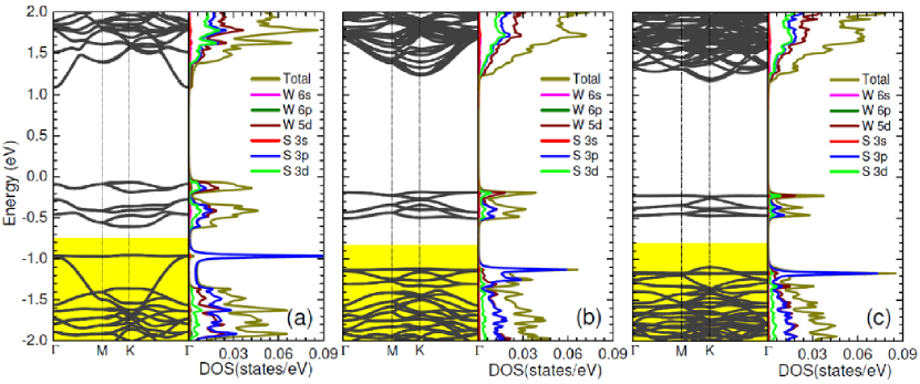
Comparing Fig. 3 with Fig. 4, we find that the Fermi energy in both MoS2 and WS2 monolayers is shifted down in energy by the presence of metal vacancies. This suggests that the Mo/W point defects can make the system a p-type semiconductor, in agreement with DFT results Lu . Moreover, the defect states of WS2 are closer to VBM than that of MoS2 monolayer, indicating that the WS2 monolayer may act as a more efficient p-type semiconductor than MoS2, when the metal vacancies are induced.
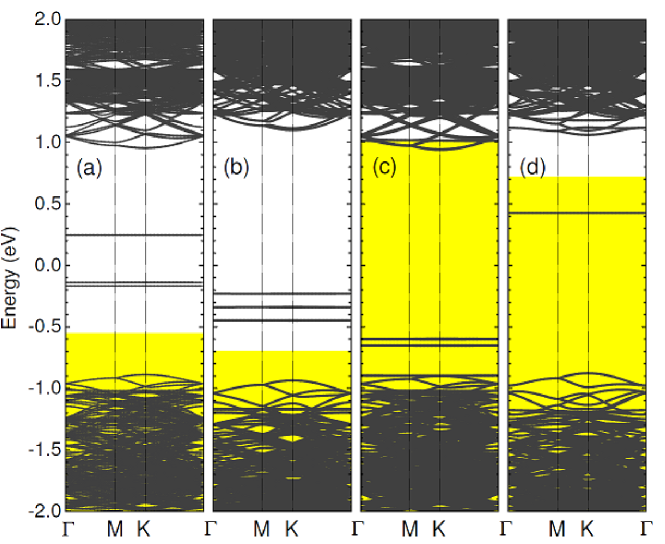
Let us study the influence of chalcogen defect on the electronic structure of the monolayers. Figs. 5 and 6 show the band structures and the partial DOS of MoS2 and WS2 monolayers, respectively, when a single sulphur vacancy (Fig. 1(b)) is created per supercell. From Fig. 5(a) it is evident that at high defect concentration, the sulphur vacancies induce a midgap band with bandwidth eV in the vicinity of the VBM, indicating that the defect states tend to be more delocalized due to the interaction between S vacancies. The midgap band manifests itself as defect states with three peaks in partial DOS which become more localized as the concentration decreases (Figs. 5(b) and 5(c)). In addition, there is a flat band just below the MoS2 CBM which does not change notably with the concentration changes. The Mo orbitals around the vacancies play the main role in creation of midgap states, while the S and orbitals do not contribute considerably to the defect states of gap region. The presence of sulphur vacancy shifts the Fermi level to the bottom of the conduction band due to unsaturated electrons in the Mo orbitals around the vacancy defect. This property suggests that sulphur vacancies can turn the MoS2 monolayers into a n-type semiconductor in agreement with theory and experiment Radisavljevic ; Liu2 ; Lu ; Qiu .
On the other hand, the electronic band structure of WS2 monolayer in the presence of sulphur vacancies with concentration shows a narrow band with bandwidth eV in the gap region (Fig. 6(a)). In this case the contribution of W orbitals and S and orbitals in generation of midgap states are almost the same, as shown in the partial DOS of Fig. 6(a). As the size of the supercell increases, the defect state in the bandgap becomes more localized around the vacancy region and the contribution of W states dominates in the localized state as can be seen in the DOS of Figs. 6(b) and 6(c). The defect state which acts as a donor level, lies about 0.6 eV below the CBM, in agreement with the DFT result Wei , indicating that at a high enough temperature some of the localized charges can be transferred to the CBM and therefore increase the system conductivity. Accordingly, we conclude that the sulphur vacancies act as electron donors and make the both MoS2 and WS2 monolayers electron rich. Besides the monosulphur vacancies, the effect of two neighboring sulphur (disulphur) vacancies on the same side of the monolayers, and also on different sides of the monolayer, but on top of each other per supercell on the electronic properties of the layers was also examined (not shown here). Our TB calculations showed an additional shift of Fermi level toward conduction band with an increase in the number of localized states in the bandgap. The experimental observations have demonstrated that these disulphur vacancies are less probable to create, due to their formation energy which is roughly twice of that of the monosulphur defect Zhou ; Hong .

Comparing the localized donor states and the Fermi energy in Figs. 5 and 6, it is clear that the n-type semiconducting behavior in MoS2 is more dominant than that in WS2, when the sulphur vacancies are introduced. This feature is in agreement with the recent experimental observation of electronic properties of MoS2-WS2 heterostructures, indicating that both MoS2 and WS2 act as n-type semiconductors with relatively high Fermi level in MoS2 as compared to WS2 Chen .
To show the advantage of our tight-binding method over first-principles calculations, we have also studied the vacancy defects in the 1111 supercells which correspond to vacancy concentration of cm-2. The electronic structure of both MoS2 and WS2 monolayers with such a low concentration of sulphur and metal defects are shown in Fig. 7. Due to this low density of defects, the vacancy-vacancy interaction is quite negligible and hence the midgap states are strongly localized. Comparing Fig. 7 with Figs. 3-6, we see that the p-type and n-type semiconducting behaviors in these defective monolayers are not affected by the value of defect concentration. Therefore, it is evident that this size of supercell is computationally trivial for our tight-binding scheme, but extremely expensive for DFT methods.
It is important to point out that the calculation of spin-dependent density of states in the close proximity of sulphur and metal defects did not show any spin polarization, indicating that in the present approximation, the single S, Mo, and W vacancies do not induce any magnetic moments.
Finally, we would like to emphasize that the agreement between the results of our Slater-Koster tight-binding model and the first-principles calculations in predicting p-type and n-type semiconducting behaviors is related to the accuracy and reliability of fitted parameters which provide us a more accurate description of the band structures, as shown in Fig. 2. Accordingly, our method is not only able to clearly demonstrate the electronic band structure of defective MoS2 and WS2 monolayers, but also is very computationally affordable and can be easily generalized to study very large systems with a random distribution of single defects and other types of vacancies such as MoS double vacancies, MoS2 triple vacancies and antisite defects Hong ; Ataca .
IV conclusion
Using Slater-Koster tight-binding model with non-orthogonal orbitals and including the spin-orbit coupling, we have explored the effect of atomic vacancies on electronic structure of MoS2 and WS2 monolayers. The vacancy defects mainly create localized states within the bandgap of pristine MoS2 and WS2, along with a shift in the Fermi energy toward VBM or CBM. As a result, the electronic properties of these monolayers are strongly affected by the introduction of atomic defects. Our results show that metal vacancies have potential to make the monolayers p-type semiconductors, while the sulphur vacancies turn the system as a n-type semiconductor.
Localization of midgap states by decreasing the defect concentration in both metal and chalcogen vacancies suggests that point defects in MoS2 and WS2 can act as resonant scatterers Chen2 ; Saffar1 . Moreover, the vacancy-induced localized states have the potential to activate new optical transitions with energies less than energy gap in their optical spectrum, suggesting a potential application of LTMDs for optoelectronic devices.
Acknowledgement
We are very grateful to F. Zahid and L. Liu for providing us the WS2 parameters and for valuable comments. This work is partially supported by Iran Science Elites Federation.
References
- (1) Q. H. Wang, K. Kalantar-Zadeh, A. Kis, J. N. Coleman, and M. S. Strano, Nat. Nanotech. 7, 699 (2012).
- (2) C. Ataca, H. Sahin, and S. Ciraci, J. Phys. Chem. C 116, 8983 (2012).
- (3) B. Radisavljevic, A. Radenovic, J. Brivio, V. Giacometti, and A. Kis, Nat. Nanotechnol. 6, 147 (2011).
- (4) D. Braga, I.G. Lezama, H. Berger, and A. Morpurgo, Nano Lett. 12, 5218 (2012).
- (5) Y. Jing, X. Tan, Z. Zhou, and P. Shen, J. Mater. Chem. A 2, 16892 (2014); Y. Li, D. Wu, Z. Zhou, C.R. Cabrera, and Z. Chen, J. Phys. Chem. Lett. 3, 2221 (2012); Y. Li, Z. Zhou, S. Zhang, and Z. Chen, J. Am. Chem. Soc. 130, 16739 (2008); Y. Jing, Z. Zhou, C.R. Cabrera, and Z. Chen, J. Mater. Chem. A 2, 12104 (2014); Q. Tang, Z. Zhou, and Z. Chen, WIREs Comput. Mol. Sci. 5, 360 (2015).
- (6) K.S. Novoselov, D. Jiang, F. Schedin, T.J. Booth, V.V. Khotkevich, S.V. Morozov, A.K. Geim, Proc. Natl. Acad. Sci. USA. 102, 10451 (2005).
- (7) W. Zhang, C.P. Chuu, J.K. Huang, C.H. Chen, M.L. Tsai, Y.H. Chang, C.T. Liang, Y.Z. Chen, Y.L. Chueh, J.H. He, M.Y. Chou and L.J. Li, Sci. Rep. 4, 3826 (2014).
- (8) G. Eda, H. Yamaguchi, D. Voiry, T. Fujita, M. Chen, M. Chhowalla, Nano Lett. 11, 5111 (2011).
- (9) J. Kang, S. Tongay, J. Zhou, J. Li, and J. Wu, Appl. Phys. Lett. 102, 012111 (2013).
- (10) K. Kośmider and J. Fernández-Rossier, Phys. Rev. B 87, 075451 (2013).
- (11) K. Chen, X. Wan, J. Wen, W. Xie, Z. Kang, X. Zeng, H. Chen, and J.B. Xu, ACS Nano 9, 9868 (2015).
- (12) Y. Yoo, Z.P. Degregorio, and J.E. Johns, J. Am. Chem. Soc. 137, 14281 (2015).
- (13) Y. Gong, J. Lin, X. Wang, G. Shi, S. Lei, Z. Lin, X. Zou, G. Ye, R. Vajtai, B.I. Yakobson, H. Terrones, M. Terrones, B.K. Tay, J. Lou, S.T. Pantelides, Z. Liu, W. Zhou, and P.M. Ajayan, Nat. Mate. 13, 1135 (2014).
- (14) S. Tongay, J. Suh, C. Ataca, W. Fan, A. Luce, J.S. Kang, J. Liu, C. Ko, R. Raghunathanan, J. Zhou, F. Ogletree, J. Li, J.C. Grossman and J. Wu, Sci. Rep. 3, 2657 (2013).
- (15) W. Zhou, X. Zou, S. Najmaei, Z. Liu, Y. Shi, J. Kong, J. Lou, P.M. Ajayan, B.I. Yakobson, and J.-C. Idrobo, Nano Lett. 13, 2615 (2013).
- (16) A.N. Enyashin, M. Bar-Sadan, L. Houben, and G. Seifert, The J. Phys. Chem. C 117, 10842 (2013).
- (17) M. Ghorbani-Asl, A.N. Enyashin, A. Kuc, G. Seifert, and T. Heine Phys. Rev. B 88, 245440 (2013).
- (18) J. Hong, Z. Hu, M. Probert, K. Li, D. Lv, X. Yang, L. Gu, N. Mao, Q. Feng, L. Xie, J. Zhang, D. Wu, Z. Zhang, C. Jin, W. Ji, X. Zhang, J. Yuan, and Z. Zhang, Nat. Commun. 6, 6293 (2015).
- (19) C. Ataca and S. Ciraci, J. Phys. Chem. C 115, 13303 (2011).
- (20) Y. Ma, Y. Dai, M. Guo, C. Niu, J. Lu, and B. Huang, Phys. Chem. Chem. Phys. 13, 15546 (2011).
- (21) H.-P. Komsa, J. Kotakoski, S. Kurasch, O. Lehtinen, U. Kaiser, and A.V. Krasheninnikov, Phys. Rev. Lett. 109, 035503 (2012).
- (22) J.-w. Wei, Z.-w. Ma, H. Zeng, Z.-y. Wang, Q. Wei, and P. Peng, AIP Adv. 2, 042141 (2012).
- (23) G.-B. Liu, W.-Y. Shan, Y. Yao, W. Yao and D. Xiao, Phys. Rev. B 88, 085433 (2013).
- (24) Y. Zhou, P. Yang, H. Zu, F. Gao, and X. Zu, Phys. Chem. Chem. Phys. 15, 10385 (2013).
- (25) B. Huang, M. Yoon, B. G. Sumpter, S.-H. Wei, and F. Liu, Phys. Rev. Lett. 115, 126806 (2015).
- (26) S. Yuan, R. Roldán, M.I. Katsnelson, and F. Guinea, Phys. Rev. B 90, 041402(R) (2014).
- (27) D. Xiao, G-B Liu, W. Feng, X. Xu and W. Yao, Phys. Rev. Lett. 108, 196802 (2012).
- (28) H. Rostami, A.G. Moghaddam and R. Asgari, Phys. Rev. B 88, 085440 (2013).
- (29) F. Zahid, L. Liu, Y. Zhu, J. Wang, and H. Guo, AIP Adv. 3, 052111 (2013).
- (30) E. Cappelluti, R. Roldán, J. A. Silva-Guillén, P. Ordejón and F. Guinea, Phys. Rev. B 88, 075409 (2013).
- (31) R. Roldán, M. P. López-Sancho, F. Guinea, E Cappelluti, J. A. Silva-Guillén, and P. Ordejón, 2D Materials 1, 034003 (2014).
- (32) J. C. Slater and G. F. Koster, Phys. Rev. 94, 1498 (1954).
- (33) F. Zahid and L. Liu, private communication.
- (34) D. A. Papaconstantopoulos and M. J. Mehl, J. Phys.: Condens. Matter 15, R413 (2003).
- (35) S. Datta, Quantum Transport: Atom to Transistor (Cambridge University Press, Camberige, 2005) ch. 5.
- (36) M. P. López Sancho, J.M. López Sancho, and J. Rubio, J. Phys. C 18, 1803 (1985).
- (37) W. Feng, Y. Yao, W. Zhu, J. Zhou, W. Yao, and D. Xiao, Phys. Rev. B 86, 165108 (2012).
- (38) K.F. Mak, C. Lee, J. Hone, J. Shan, and T.F. Heinz, Phys. Rev. Lett. 105, 136805 (2010).
- (39) L.F. Mattheiss, Phys. Rev. Lett. 30, 784 (1973); Phys. Rev. B 8, 3719 (1973).
- (40) D. Wickramaratne, F. Zahid, and R.K. Lake, J. Chem. Phys. 140, 124710 (2014).
- (41) M. Gibertini, F.M.D. Pellegrino, N. Marzari, Marco Polini, Phys. Rev. B 90, 245411 (2014).
- (42) S.-C. Lu and J.-P. Leburton, Nano. Res. Lett. 9, 676 (2014).
- (43) D. Liu, Y. Guo, L. Fang, and J. Robertson, Appl. Phys. Lett. 103, 183113 (2013).
- (44) H. Qiu, T. Xu, Z. Wang, W. Ren, H. Nan, Z. Ni, Q. Chen, S. Yuan, F. Miao, F. Song, G. Long, Y. Shi, L. Sun, J. Wang and X. Wang, Nat. Comm. 4, 2642 (2013).
- (45) J.-H. Chen, L. Li, W.G. Cullen, E.D. Williams, and M.S. Fuhrer, Nat. Phys. 7, 535 (2011).
- (46) A. Saffarzadeh and G. Kirczenow, Phys. Rev. B 90, 155404 (2014).