Tuning optical properties of Ge nanocrystals by Si shell
Abstract
We present a theoretical study of Ge-core/Si-shell nanocrystals in a wide bandgap matrix and compare the results with experimental data obtained from the samples prepared by co-sputtering. The empirical tight-binding technique allows us to account for the electronic structure under strain on the atomistic level. We find that a Si shell as thick as 1 monolayer is enough to reduce the radiative recombination rate as a result of valley cross-over. Thin Si shell leads to a dramatic reduction of the optical bandgap from visible to near-infrared range, which is promising for photovoltaics and photodetector applications.
Our detailed analysis of the structure of the confined electron and hole states in real and reciprocal spaces indicates that the type-II heterostructure is not yet achieved for Si shells with the thickness below 0.8 nm, despite some earlier theoretical predictions. The energy levels of holes are affected by the Si shell stronger than the electron states, even though holes are completely confined to the Ge core. This occurs probably due to a strong influence of strain on the band offsets.
I Introduction
Ge nanostructures are of great interest for light emitter/detector applications in optoelectronics, photonics and photovoltaics.Süess et al. (2013) The indirect bandgap -vector selection rules are lifted in nanostructures by quantum confinement, promising greatly enhanced radiative rate and size-tunable bandgap.Niquet et al. (2000); Bostedt et al. (2004); Bulutay (2007); Sevik and Bulutay (2008); Ossicini et al. (2010) Unfortunately, Ge nanocrystals (NCs) naturally oxidize upon exposure to air, leading to formation of O-related centers that act either as radiative centers with fast decaying blue-green emission Maeda (1995); Takeoka et al. (1998); Niquet et al. (2000); Chivas et al. (2011) or as defect traps dramatically reducing emission (see e.g. remarks in Ref. Niquet et al., 2000). Despite these difficulties, Ge nanostructures remain of great interest, showing attractive properties like highly efficient space separated multiple exciton generation (MEG).Saeed et al. (2014a) Moreover, for integrated optoelectronics and photonics development, Ge remains to be cheaper and more CMOS compatible counterpart to Si than III-V and II-VI semiconductors.
A possible route to further advanced material properties engineering is alloying and straining of Ge by Si by developing various Si/Ge nano-heterostructures.d’Avezac et al. (2012); Zhang et al. (2012) Alloying Ge with Si allows one to tune bandstructure and bandgap into almost optimal range for photovoltaics employing carrier multiplication.Kolodinski et al. (1995); Wolf et al. (1998); J. H. Werner (1994) Tensile straining of Ge can lead to modified band structure towards direct bandgap,Van de Walle (1989); Huo et al. (2011); Jain et al. (2012); Süess et al. (2013) which is more pronounced compared to Si, due to a small energy difference between the direct – and the indirect (–) transitions. Possible routes towards permanent straining are core-shell type heterostructures, such as nanowires or nanocrystals. Si and Ge form type-II heterostructures and it is natural to expect that in the Si/Ge-based nanostructures the holes are localized in the Ge region and electrons in the Si region. However, there is a lattice mismatch of 4% between the Si and Ge, and consequently, band alignment is modified by the strain. Ge NCs capped with thin Si shell are also promising because Si acts as a protective coating, eliminating formation of the GeO oxide layer,Liu et al. (2008) source of emissive defect centers Min et al. (1996); Wu et al. (1999) and/or emission quenching.Takeoka et al. (2000a) Type-II heterostructures are in general interesting for photodetectors and memory applications Liu et al. (2008) due to lowered rates of optical transitions, as spatially separated electron and hole recombine less efficiently. Also, photon absorption process is typically controlled by the core-core or shell-shell transition, that is energetically shifted from the core-shell emission. Hence, such system also provides transparency for emission due to the lack of reabsorption, interesting for amplifiers and lasers. Core-shell scheme can also lead to reduced blinking Galland et al. (2012) and single exciton population inversion.Klimov et al. (2007)
Quite recently, unusually bright and fast decaying (1 ns) photoluminescence (PL) has been reported from co-sputtered Ge and Si-rich SiO2.Saeed et al. (2014b) Three-component PL has been observed, strongly suggesting formation of type-II core-shell heterostructure, however, this suggestion was not confirmed. The properties of such core-shell nanocrystals were discussed in the literature mostly based on approach that lacks sensitivity to valley-dependent phenomena, crucial in understanding the electronic structure of the system. Also, not much emphasis has been put on complex strain in the realistic nanocrystals which could further obscure the details of their electronic structure.
The ways to prepare well-defined core-shell Si/Ge or Ge/Si NC systems are relatively scarce. In past, various techniques were used, such as mechanical alloying by ball milling,Wang et al. (2008) wet chemical etching Malachias et al. (2003) and molecular beam epitaxy,Alonso et al. (2005); Valakh et al. (2005); Demchenko et al. (2007) wet chemical synthesis Yang et al. (1999); Barry et al. (2011), synthesis from gas phase (silane and germane) Pi and Kortshagen (2009); Erogbogbo et al. (2011); Yasar-Inceoglu and Mangolini (2013); Mehringer et al. (2015) and co-sputtering.Takeoka et al. (2000b); Buljan et al. (2010); Kolobov et al. (2002) The segregation of Ge and Si is often the case for Ge-rich SiGe alloys, even though miscibility of Ge and Si is expected for whole compositional range. It has been shown both theoretically and experimentally that Si-capped Ge NCs have formation energies similar to those of Ge NCs with the same number of atoms, while Ge-capped Si NCs are less stable than Si NCs.Ramos et al. (2005) For samples with high Ge content prepared by radio frequency (RF) magnetron co-sputtering and annealed at high temperatures, composite NCs consisting of a Ge NC core and amorphous SiGe shell have been reported from the Raman analysis.Kolobov et al. (2002); Yang et al. (2004) Currently, the best evidence for formation of Ge-core/Si-shell systems has been provided by M. Buljan using co-sputtering technique and X-ray analysis.Buljan et al. (2010)
Available Density Functional Theory (DFT) calculations of small core-shell Si/Ge and Ge/Si NC systems by Ramos et al. Ramos et al. (2005) and Oliveira et al. de Oliveira et al. (2012) predict type-II confinement with holes in Ge and electrons in Si. Si/Ge core-shell system is shown to offer high oscillator strength and long decay time, but large shift of absorption threshold with varying Ge shell thickness. Ge/Si core-shell, on the other hand shows long lifetimes with lower absorption shifts, making this material more suitable for e.g. photodetectors. For larger Si/Ge and Ge/Si core-shell NC systems, tight binding calculations are available by Neupane et al. Neupane et al. (2011, 2015), however, with limited scope: study of carriers in Ge/Si core-shell system with thick fixed shell thickness of 5 nm Neupane et al. (2011) and in large Ge/Si dome-shaped nanostructures with the base diameters in the range nm.Neupane et al. (2015) In our work we address the missing category of larger Ge NC core with thin Si shell: system that can be relatively simply prepared by chemical synthesis Yang et al. (1999) or sputtering.Buljan et al. (2010) New tools have been developed to trace real- and -space origin for each quantum-confined state. Using these tools we show that Ge optical properties can be extensively tuned by adding relatively thin Si shell.
II Tight-binding model
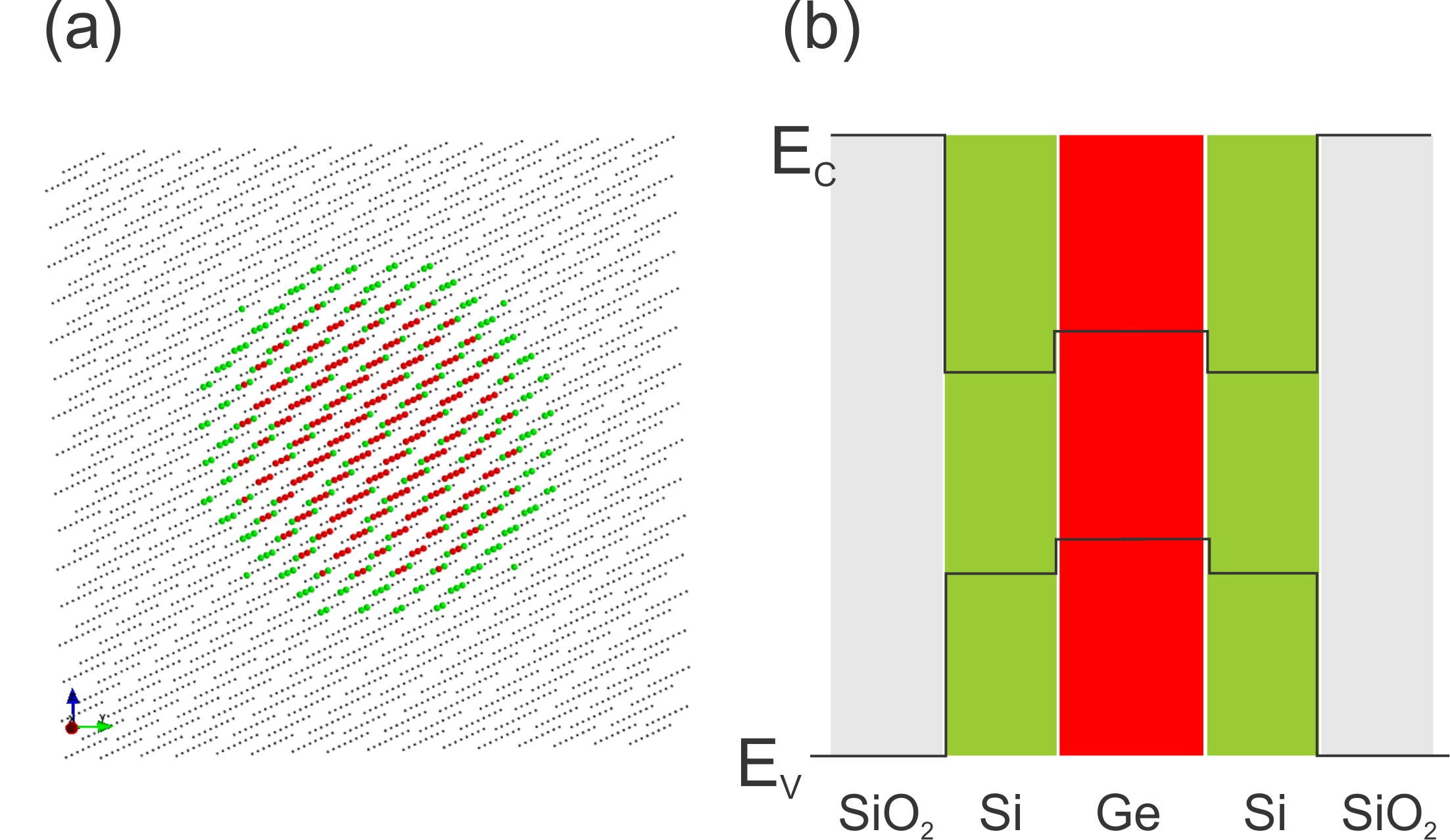
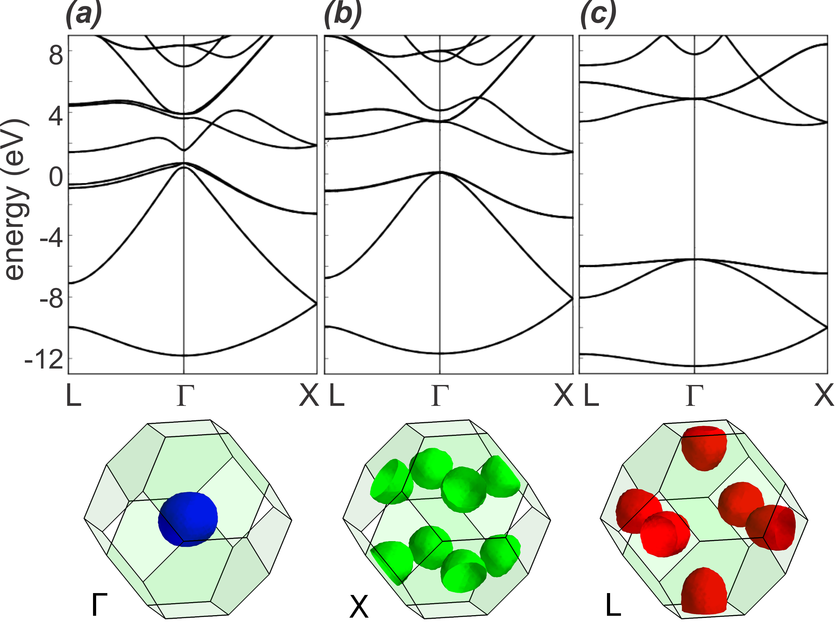
The structure under consideration is schematically shown in Fig. 1(a). It consists of a Ge nanocrystalline core with the diameter (red atoms), and crystalline Si shell with the diameter (green atoms) embedded in the amorphous SiO2 matrix (gray atoms). The atomic coordinates between Si and SiO2 were relaxed according to the standard valence force field (VFF) theoryKeating (1966) in order to minimize the strain energy. This approach is reasonable for covalent semiconductors and provides atomistic strain with relatively high precision.Rücker and Methfessel (1995) We model SiO2 as a virtual crystal with zincblende lattice, with bandstructure near band gap similar to -quartz. In order to describe nominally unstrained core-shell Si/Ge NC, we set the VFF parameters to mimic soft material. The electronic spectrum has been obtained using the standard empirical tight-binding (TB) techniqueJancu et al. (1998) and parametrization.Niquet et al. (2009) Since there is no universally accepted TB parametrization of -SiO2 in literature,Tu and Tersoff (2000); Watanabe et al. (2010) we have considered SiO2 phenomenologically, with TB parameters manually chosen to reproduce the experimental band gap and offsets.Bulutay (2007) The valence and conduction band offsets between Si, Ge and SiO2 lead to the type-II heterostructure system, the schematic band diagram is depicted in Fig. 1(b). The tight-binding parameters used are given in supplementary material. The corresponding TB band structures of bulk Ge, Si and SiO2 are shown in Fig. 2(a-c), respectively. The bulk Si and Ge have quite different band structures with the conduction band minima located in the and valleys, respectively. The valence band extrema, however, are in the point for all considered materials.
NC have discrete set of eigenstates with energy and wavefunction . The TB wavefunction of -th state (we will omit it below when this does lead to confusion)
| (1) |
is determined by a set of complex coefficients defined on a lattice in 3D space. The index labels the orbital and spin degrees of freedom of the atomic-like wavefunctions . Tight-binding wave functions are hard to analyze without a postprocessing that extracts physically relevant quantities. An obvious example is the real space distribution of electron density: local density of states (LDOS) which we define as
| (2) |
where are the tight-binding coefficients at -th atom, is Gaussian broadening which may be chosen to be of the order of interatomic distance and is the position of -th atom. Equation (2) for LDOS allows one to trace the real space distribution of the electron density for the particular state. However, LDOS only is not enough to visualize all the features of electron states. In order to trace the valley structure of the states, below we define k-space LDOS. For this, we perform a Fourier transform of the TB wavefunction of confined carriers as explained below. For a given lattice one can formally define a lattice in the reciprocal space.Bricogne (2006) For the finite system we consider a large supercell and apply periodic boundary conditions. The supercell is defined as a parallelogram cut from ideal zincblende lattice by vectors . This parallelogram defines a lattice in the reciprocal space with the basis vector
| (3) |
and , are obtained by the cyclic permutations.
Positions of cations in the ideal lattice are defined as
| (4) |
where are the standard basis vectors of face-centered cubic lattice and anions are shifted by the vector . The vectors correspond to the reciprocal space vectors
| (5) |
The vectors form the basis of another lattice in the reciprocal space associated with the crystal lattice. The first Brillouin zone of the lattice is defined by the supercell vectors by considering vectors equal if and only if they are differ by a linear combination of . We will call this set of vectors “k-space mesh”
| (6) |
Simple linear algebra shows that the number of vectors in the first Brillouin zone is exactly equal to the number of prime cells in a supercell bounded by the vectors . Definition of the vectors , , and is illustrated in Fig. 3. With these definitions we introduce a discrete Fourier transform by
| (7) |
that gives us the same number of coefficients as we had in the TB wavefunction in real space. The sum in Eq. (7) runs through atoms in two sublattices separately. This formal definition satisfies the obvious properties one could expect from a function in reciprocal space: the norm is conserved, the orthogonality of the states is preserved. If one considers the state with well-defined wave vector , the corresponding Fourier transform has a sharp maximum for . This allows us to attribute the confined states to particular valleys.
Similar to LDOS in real space Eq. (2) we may define LDOS in reciprocal space, which we will call k-space LDOS or kLDOS below, as
| (8) |
where the -space Gaussian smoothing parameter is conveniently chosen of the order of . To illustrate this procedure, Fig. 2(d) presents the isodensity surface plots of -space LDOS calculated using Eq. (8) for few particular states which show definite , and valley character for a realistic calculations of NCs, see below. It can be seen that the kLDOS indeed clearly shows the valley structure.
Importantly, this approach can be formally used for strained structures as well, although care is needed. When the strain is applied, atomic positions start to deviate from ideal crystal lattice and a proper generalization of the above scheme must be used. The approach outlined above is closely related with the unfolding scheme used in Ref. Hapala et al., 2013 and up to some generalizations and approximations it is equivalent to the unfolding scheme proposed in Refs. Boykin and Klimeck, 2005; Boykin et al., 2007; Popescu and Zunger, 2010, 2012, but the detailed comparison is out of the scope of the current paper.
III Results for varying core and shell thicknesses
Now we proceed to the detailed analysis of influence of the crystalline Si shell on electronic structure and density of states (DOS) re-distribution with respect to the Ge NC without shell. We have simulated many different systems that can be separated into two major groups: (a) systems with fixed Ge NC core diameter to 2.9 nm and variable shell of the thickness 0, 0.12, 0.25, 0.54, 0.78, 0.93 and 1.06 nm; (b) set of five different Ge NC core sizes of 1.50, 1.75, 2.25, 2.75 and 3.50 ML (monolayers), which corresponds to 1.7, 2.0, 2.5, 3.1 and 3.9 nm core diameter, each studied for a set of Si shell thicknesses of 0, 0.12, 0.54 and 0.80 nm. More details on the second set can be found in the Supplementary Information. We model SiO2 as a soft material, as a result the strain at the NC surface is relaxed. However, the strain between the Ge core and Si shell (which roughly results in compression of Ge core and stretching of Si shell) is fully included in the simulations and contributes to modifications in the band structure.
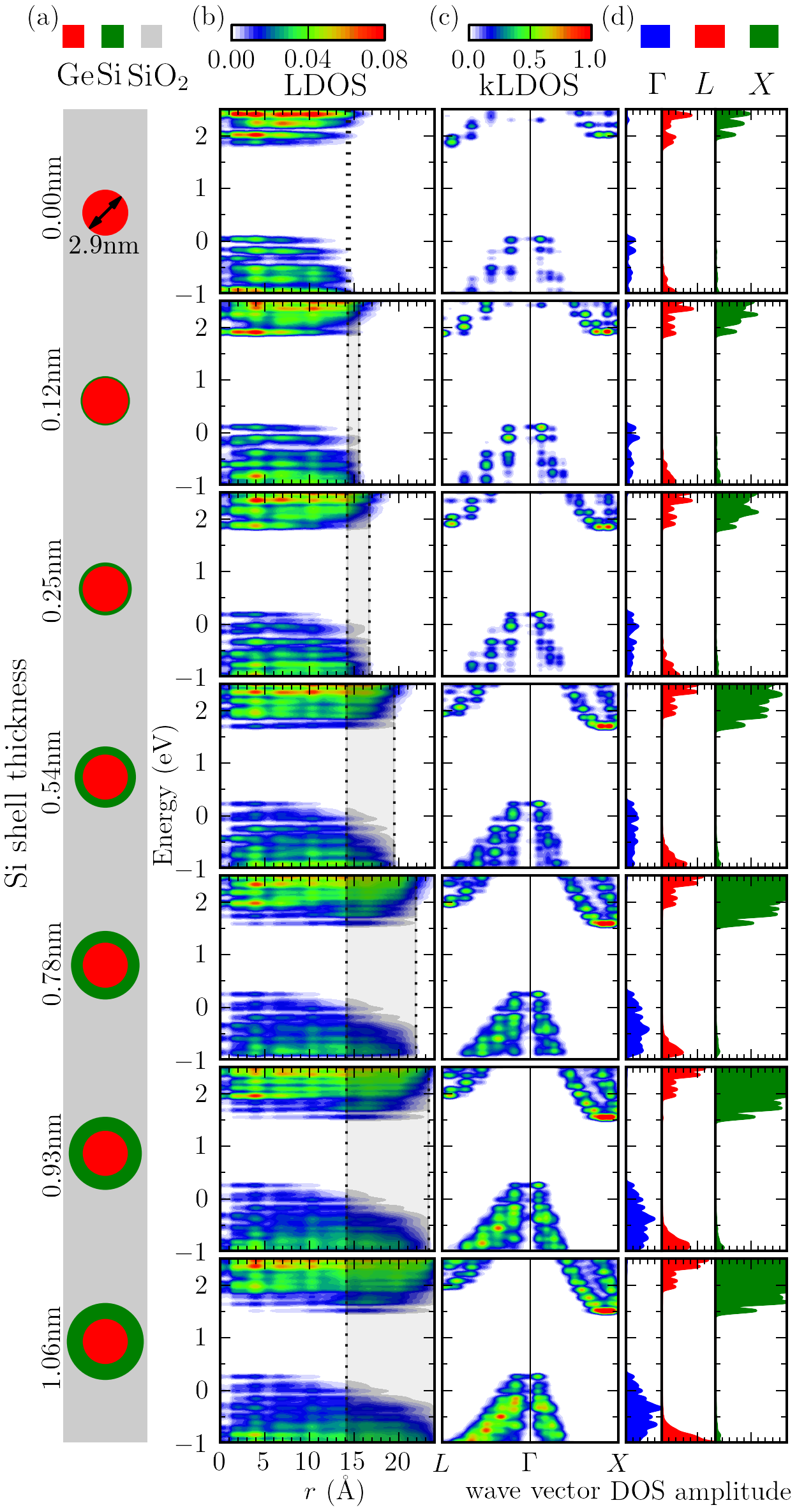
First we will study fixed Ge NC core size of 3.1 nm with the Si shell varied between 0 and 1.30 nm (see Fig. 4(a)). Figure 4(b) presents the energy-resolved LDOS for hole and electron states in the radial direction,
| (9) |
where the index enumerates the atoms with the distance to the QD center , enumerates different solutions with the energies and two broadening parameters Å and meV. An extra factor is added to (9) to produce the values analogous to the regular DOS that satisfy the condition . Color indicates high (red) to low (blue) DOS and the vertical gray lines denote edges of the core and the shell, respectively, with the shell area shown by the gray rectangle. As expected, for thicker Si shell, electrons become localized in the shell, however, due to small energy offset between Si and Ge conduction band minima, the localization degree is relatively weak.
It is instructive to analyze the microscopic structure of the confined states also in the wave-vector space. This can be shown by examining the energy-resolved k-space LDOS (the term “fuzzy band structure” has been used in Ref. Hapala et al., 2013) which is calculated as:
| (10) |
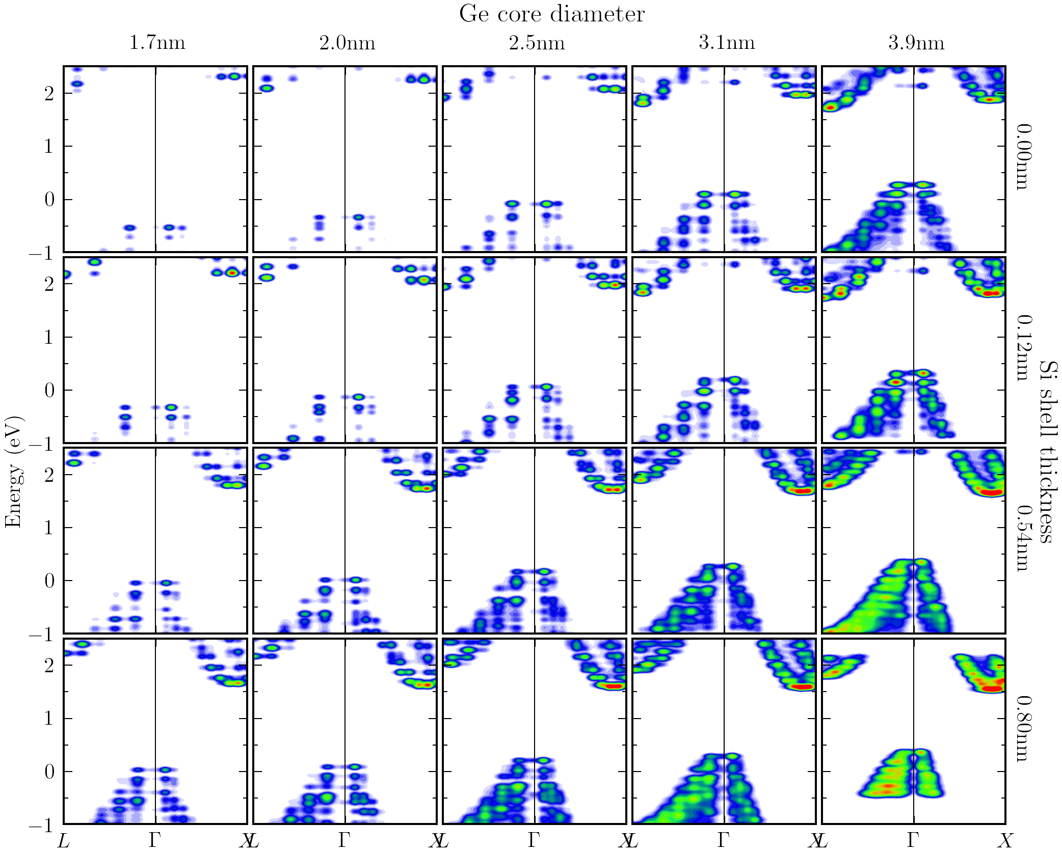
where Å-1 and meV. Then we fold k-space onto irreducible part of the Brilllouin zone using its point symmetry and take the 2D slice of the function with running along the –– path in reciprocal space as “” axis and energy as “” component. Note that we do not consider integration over angle here, unlike in (9): the real space distribution of LDOS is more or less isotropic while resiprocal space LDOS is noticably localized near valley minima (see Fig. 2(d)). The results of calculation are presented in Fig. 4(c). Colors indicate high (red) to low (blue) DOS. Notably, even in this relatively small Ge NCs, the band structure retains the features of the bulk. When the Si shell thickness increases, the energy of the “-branch” slightly increases and, simultaneously, the “-branch” energy decreases, see Figs. 4(c).
In Fig. 4(d) we evaluate the valley composition of the confined states quantitatively by integrating the density in the reciprocal space in the regions near , and points. The result is a DOS in three valleys separately. Figure 4(d) shows, that the valence band states are constructed mostly from the states near point. On the other hand, the structure of the confined conduction band states changes from -valley states to an -valley states (valley cross-over) when the Si shell is added and its thickness increases. This effect is more pronounced in smaller Ge NCs and has a threshold behavior.
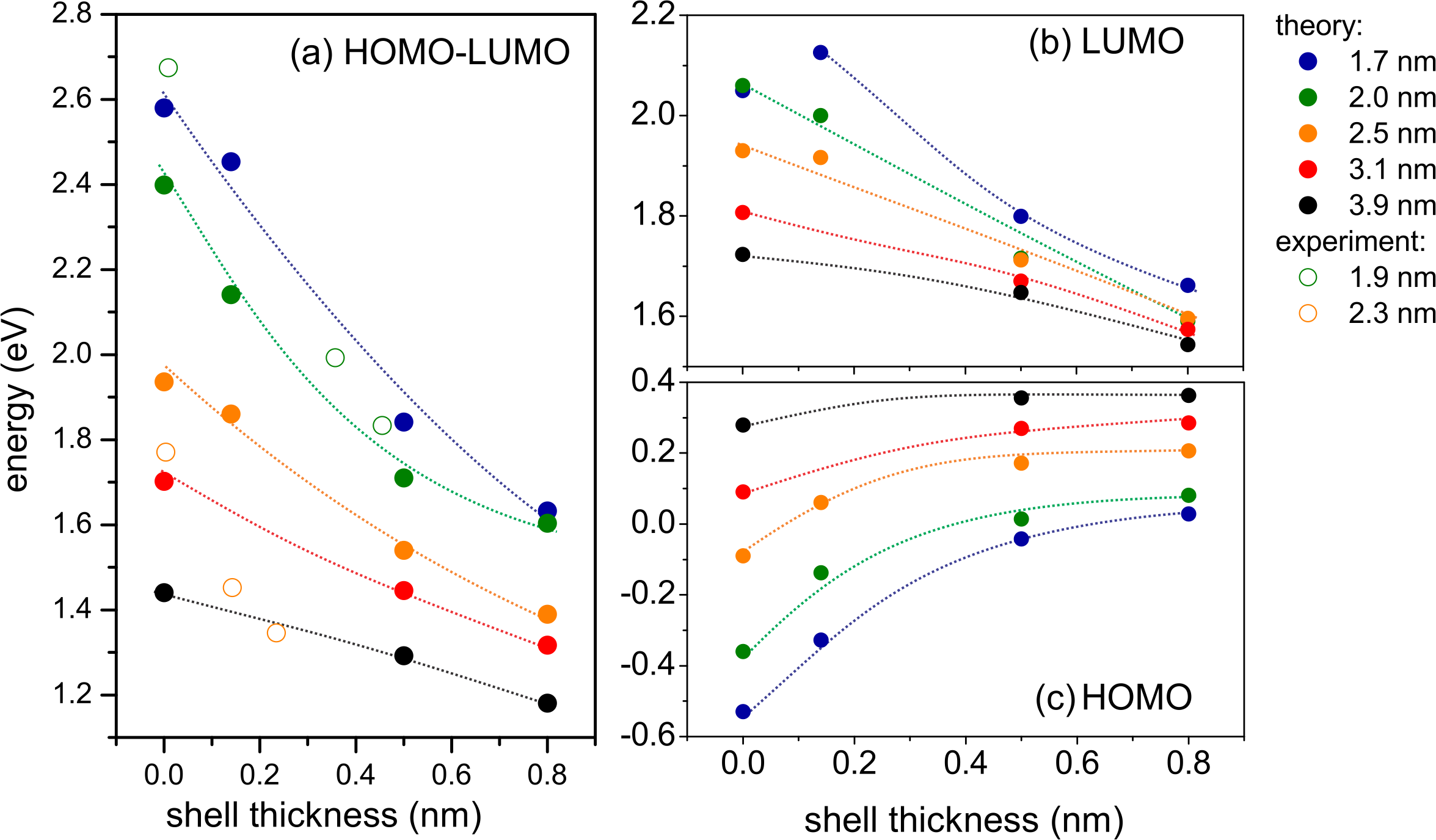
It is interesting that the Si shell leads not only to the valley cross-over for the conduction band from to , but also to a dramatic reduction in the band gap energy of the whole system. Figure 5(a) demonstrates that the NC band gap strongly decreases for larger core diameters as expected from the size quantization effect, but it is also reduced to a similar degree by adding the Si shell only. The shell-induced reduction is more pronounced for smaller NCs. Interestingly, even though holes are confined in the Ge core (Fig. 4(b)), their energy (HOMO) is more sensitive to the shell presence than that for the electronic states (LUMO), which are delocalized over the Ge core and Si shell (more localized in Si for thicker shells), see Fig. 4(b). This is related to larger band offset for the valence band than for conduction band. For thicker Si shell, the spectral tunability by Ge NC core size is reduced when compared to the systems with thinner shell. We would like to note here, that the native bandgap for uncapped Ge NCs in SiO2 here is reduced with respect to the hydrogen-capped Ge NC in vacuum, as a result of lower potential barrier at the Si/SiO2 boundary. Optical bandgap energies obtained in our model are compared in Fig. 5(a) with the experimental data obtained in the group of M. Buljan Buljan et al. (2010) from the analysis of absorption and structural properties of Ge/Si core-shell samples prepared by co-sputtering in Al2O3 matrix. The calculation in Fig. 5 has been performed for a cubic supercell with the edge length few ML larger than NC diameter (large enough to neglect tunneling through SiO2). Theoretical and experimental data appear to agree quantitatively and qualitatively for smaller Ge NCs. For larger NCs the measured band gap is smaller than that predicted here. However, we note that structures prepared by M. Buljan have not fully closed Si shell, as revealed by their in-depth structural analysis by the small-angle X-ray scattering (SAXS).Buljan et al. (2010)
Now we proceed to the analysis of the radiative recombination rates depending on the thickness of the Si shell for the 3.1 nm Ge NCs. The phonon-less optical transition rate between the electron states and in the conduction and valence bands is given by Delerue and Lannoo (2004)
| (11) |
where is the local field factor, and are the energies of the corresponding states. To account for the possible degeneracy of the states the rate Eq. (11) is to be summed over the final states with the same energy and averaged over the initial states . The velocity operator can be defined as a commutator of the tight-binding Hamiltonian with the coordinate operator, We use the diagonal approximation for the coordinate operator.Voon and Ram-Mohan (1993); Ivchenko and Nestoklon (2002); Sandu (2005) This corresponds to neglecting the intraatomic matrix elements of the velocity operator for the optical transitions, which is reasonable for covalent semiconductors.Cruz et al. (1999)
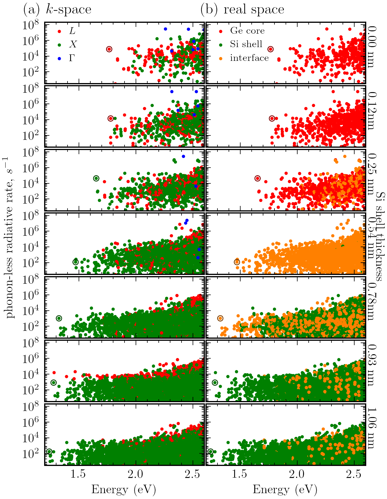
The calculated phonon-less radiative transition rates are presented in Fig. 6. Each transition is shown by a colored dot. To highlight the valley structure of the electron states, the color in Fig. 6(a) indicates the valley attribution of the state, i.e. the blue color corresponds to the electron density over 40% in the point, green to the point and red to the point. The figure clearly demonstrates the decrease of the band gap for thicker Si shell, as presented previously in Figs. 4 and 5. Also, the valley cross-over is clearly visible, as the lowest energy transitions change from L-valley (red) to X-valley (green) for thicker shell. Furthermore, addition of shell also leads to dramatic reduction in the rates, which appears to be clearly related to the modification of the -space structure of the electron states.
It is interesting to plot also the real-space-resolved transition rates (Fig. 6(b)) with the color signifying more than 40% localization of the electron density component in Ge core (red), Si shell (green) or delocalized equally in between (orange). This figure shows that even though the localization of electron in the shell in Fig. 4(b) was not clearly pronounced, the rates are already reduced for 0.5 nm-thick Si shell. As such, the rates suppression slightly precedes the over 40% localization of the electron in the shell, which occurs only for shells thicker than 0.8 nm. This means that the valley cross-over has already a strong influence on the rate reduction beyond the “standard” spatial delocalization role found in typical II-type heterostructures.
IV Conclusions
In our simulation, we present a detailed analysis of Ge/Si core-shell NC systems that can be prepared by wet chemical synthesis Yang et al. (1999) or co-sputtering.Buljan et al. (2010) New tools have been developed to trace real- and reciprocal-space origin for every transition.
Since the Si shell leads to compressive strain of Ge core, the direct bandgap cannot be induced in such structures. It has been previously shown by the DFT ab-initio simulations Ramos et al. (2005); de Oliveira et al. (2012) that the Si/Ge and Ge/Si core-shell NC systems are type-II heterostructures with electrons located in Si and holes in Ge. In our simulations for larger systems, we found that the two phenomena should be distinguished, namely the localization of an electron in the Si shell in the real space and the -to- valley crossover of the conduction band minimum in the reciprocal space. Localization in the shell is not quite distinct and can be seen only for lowest conduction band states when the shell thickness exceeds approximately 0.7 nm. On the other hand, the valley crossover is already seen for diatomic Si shell. The valence band maximum remains in the point for all simulated Si shell thicknesses. Interestingly, even though the holes reside in the Ge core, their energy (HOMO) is influenced by the Si shell more than that of electrons (LUMO). This effect is more pronounced in smaller NCs.
The crossover and associated real space localization of the wavefunction leads to a dramatic reduction in the phonon-less radiative recombination rates. Reduced rates are of interest for photodetector applications. Improved emission yield might be expected for Si-capped NCs, since reduced recombination rate also leads to reduced Auger recombination.
The emission energy of Ge QDs can be efficiently tuned by adding Si shell of variable thicknesses. For fixed NC core size, strong reduction in band gap energy was observed with thicker Si shell, from visible range towards near-infrared range, interesting for photodetectors and photovoltaics. The optical bandgap energy and shell-dependence are in a good quantitative and qualitative agreement with experimental data obtained by M. Buljan Buljan et al. (2010) from samples prepared using co-sputtering technique. For thicker Si shell, the core-size-tunability of the optical bangap is drastically reduced. This is mainly related to strain induced by the Si shell, which modifies the energy offsets of valence and conduction bands differently. This means that the otherwise steep tunability of Ge NCs can be limited by the Si shell, allowing for achieving narrower spectral range for broader-size ensemble of NCs.
In addition to the calculation presented here, the – crossover may lead to significant change of phonon-assisted transitions. In order to develop the detailed theory of optical properties of Ge/Se core-shell systems one also needs an accurate consideration of non-radiative recombination at defects in SiO2 and the renormalization of exciton energy by dielectric confinement in NC.Benchamekh et al. (2014) Both are strongly affected by Si core thickness. However, it is worth noting that the extremely long radiative decay rates presented in Fig. 6 suggest that in experiments, phonon-assisted recombination bypass phonon-less process.
Acknowledgements.
The work of MN and AP was financially supported by the Russian Science Foundation grant No. 14-12-01067. KD would like to acknowledge financial support by MacGillavry Fellowship at University of Amsterdam.References
- Süess et al. (2013) M. J. Süess, R. Geiger, R. A. Minamisawa, G. Schiefler, J. Frigerio, D. Chrastina, G. Isella, R. Spolenak, J. Faist, and H. Sigg, “Analysis of enhanced light emission from highly strained germanium microbridges,” Nature Photonics 7, 466 (2013).
- Niquet et al. (2000) Y. M. Niquet, G. Allan, C. Delerue, and M. Lannoo, “Quantum confinement in germanium nanocrystals,” Appl. Phys. Lett. 77, 1182–1184 (2000).
- Bostedt et al. (2004) C. Bostedt, T. van Buuren, T. M. Willey, N. Franco, L. J. Terminello, C. Heske, and T. Möller, “Strong quantum-confinement effects in the conduction band of germanium nanocrystals,” Applied Physics Letters 84, 4056 (2004).
- Bulutay (2007) C. Bulutay, “Interband, intraband, and excited-state direct photon absorption of silicon and germanium nanocrystals embedded in a wide band-gap lattice,” Phys. Rev. B 76, 205321 (2007).
- Sevik and Bulutay (2008) C. Sevik and C. Bulutay, Phys. Rev. B 77, 125414 (2008).
- Ossicini et al. (2010) S. Ossicini, M. Amato, R. Guerra, M. Palummo, and O. Pulci, Nanoscale Res. Lett. 5, 1637 (2010).
- Maeda (1995) Y. Maeda, Phys. Rev. B 51, 1658 (1995).
- Takeoka et al. (1998) S. Takeoka, M. Fujii, S. Hayashi, and K. Yamamoto, “Size-dependent near-infrared photoluminescence from Ge nanocrystals embedded in SiO2 matrices,” Phys. Rev. B 58, 7921–7925 (1998).
- Chivas et al. (2011) R. Chivas, S. Yerci, R. Li, L. Dal Negro, and T. F. Morse, Opt. Mater. 33, 1829 (2011).
- Saeed et al. (2014a) S. Saeed, E. M. L. D. de Jong, K. Dohnalova, and T. Gregorkiewicz, “Efficient optical extraction of hot-carrier energy,” Nature Communications 5, 4665 (2014a).
- d’Avezac et al. (2012) Mayeul d’Avezac, Jun-Wei Luo, Thomas Chanier, and Alex Zunger, “Genetic-algorithm discovery of a direct-gap and optically allowed superstructure from indirect-gap Si and Ge semiconductors,” Phys. Rev. Lett. 108, 027401 (2012).
- Zhang et al. (2012) Lijun Zhang, Mayeul d’Avezac, Jun-Wei Luo, and Alex Zunger, “Genomic design of strong direct-gap optical transition in Si/Ge core/multishell nanowires,” Nano letters 12, 984 (2012).
- Kolodinski et al. (1995) S. Kolodinski, J. H. Werner, and H.J. Queisser, Appl. Phys. A 61, 535 (1995).
- Wolf et al. (1998) M. Wolf, R. Brendel, J. H. Werner, and H. J. Queisser, J. Appl. Phys. 83, 4213 (1998).
- J. H. Werner (1994) H. J. Queisser J. H. Werner, S. Kolodinski, Phys. Rev. Lett. 72, 3851 (1994).
- Van de Walle (1989) Chris G. Van de Walle, “Band lineups and deformation potentials in the model-solid theory,” Phys. Rev. B 39, 1871–1883 (1989).
- Huo et al. (2011) Yijie Huo, Hai Lin, Robert Chen, Maria Makarova, Yiwen Rong, Mingyang Li, Theodore I. Kamins, Jelena Vuckovic, and James S. Harris, “Strong enhancement of direct transition photoluminescence with highly tensile-strained ge grown by molecular beam epitaxy,” Applied Physics Letters 98, 011111 (2011).
- Jain et al. (2012) Jinendra Raja Jain, Aaron Hryciw, Thomas M. Baer, David A. B. Miller, Mark L. Brongersma, and Roger T. Howe, “A micromachining-based technology for enhancing germanium light emission via tensile strain,” Nature Photonics 6, 398 (2012).
- Liu et al. (2008) Hai Liu, Wyatt Winkenwerder, Yueran Liu, Domingo Ferrer, Davood Shahrjerdi, Scott K. Stanley, John G. Ekerdt, and Sanjay K. Banerjee, “Core-shell germanium–silicon nanocrystal floating gate for nonvolatile memory applications,” IEEE TRANSACTIONS ON ELECTRON DEVICES 55, 2610 (2008).
- Min et al. (1996) K. S. Min, K. V. Shcheglov, C. M. Yang, H. A. Atwater, M. L. Brongersma, and A. Polman, Appl. Phys. Lett. 68, 2511 (1996).
- Wu et al. (1999) X. L. Wu, T. Gao, G. G. Siu, S. Tong, and X. M. Bao, Appl. Phys. Lett. 74, 2420 (1999).
- Takeoka et al. (2000a) S. Takeoka, K. Toshikiyo, M. Fujii, S. Hayashi, and K. Yamamoto, Phys. Rev. B 61, 15988 (2000a).
- Galland et al. (2012) Christophe Galland, Yagnaseni Ghosh, Andrea Steinbrück, Jennifer A. Hollingsworth, Han Htoon, and Victor I. Klimov, “Lifetime blinking in nonblinking nanocrystal quantum dots,” Nature Communications 3, 908 (2012).
- Klimov et al. (2007) Victor I. Klimov, Sergei A. Ivanov, Jagjit Nanda, Marc Achermann, Ilya Bezel, John A. McGuire, and Andrei Piryatinski1, “Single-exciton optical gain in semiconductor nanocrystals,” Nature 447, 441 (2007).
- Saeed et al. (2014b) Saba Saeed, Frank Buters, Katerina Dohnalova, Lech Wosinski, and Tom Gregorkiewicz, “Structural and optical characterization of self-assembled ge nanocrystal layers grown by plasma-enhanced chemical vapor deposition,” Nanotechnology 25, 405705 (2014b).
- Wang et al. (2008) X. W. Wang, H. Lee, Y. C. Lan, G. H. Zhu, G. Joshi, D. Z. Wang, J. Yang, A. J. Muto, M. Y. Tang, J. Klatsky, S. Song, M. S. Dresselhaus, G. Chen, and Z. F. Ren, Appl. Phys. Lett. 93, 193121 (2008).
- Malachias et al. (2003) A. Malachias, S. Kycia, G. Medeiros-Ribeiro, R. Magalhaes-Paniago, T. I. Kamins, and R. S. Williams, Phys. Rev. Lett. 91, 176101 (2003).
- Alonso et al. (2005) M. I. Alonso, M. D. Calle, J. O. Osso, M. Garriga, and A. R. Goni, J. Appl. Phys. 98, 033530 (2005).
- Valakh et al. (2005) M. Y. Valakh, V. O. Yukhymchuk, V. M. Dzhagan, O. S. Lytvyn, A. G.Milekhin, O. P. Pchelyakov, F. Alsina, and J. Pascual, Nanotechnology 16, 1464 (2005).
- Demchenko et al. (2007) I. N. Demchenko, K. Lawniczak-Jablonska, S. Kret, A. V. Novikov, J. Y. Laval, M. Zak, A. Szczepanska, A. N. Yabloskiy, and Z. F. Krasilnik, Nanotechnology 18, 115711 (2007).
- Yang et al. (1999) C.-S. Yang, S. Kauzlarich, and Y. C. Wang, Chem. Mater. 11, 3666 (1999).
- Barry et al. (2011) S. D. Barry, Z. Yang, J. A. Kelly, E. J. Henderson, and J. G. C. Veinot, Chem. Mater. 23, 5096 (2011).
- Pi and Kortshagen (2009) X. D. Pi and U. Kortshagen, Nanotechnology 20, 295602 (2009).
- Erogbogbo et al. (2011) F. Erogbogbo, T. Liu, N. Ramadurai, P. Tuccarione, L. Lai, M. T. Swihart, and P. N. Prasad, ACS Nano 5, 7950 (2011).
- Yasar-Inceoglu and Mangolini (2013) O. Yasar-Inceoglu and L. Mangolini, Mater. Lett. 101, 76 (2013).
- Mehringer et al. (2015) Christian Mehringer, Christian Kloner, Benjamin Butz, Benjamin Winter, Erdmann Spiecker, and Wolfgang Peukert, “Germanium-silicon alloy and core-shell nanocrystals by gas phase synthesis,” Nanoscale 7, 5186–5196 (2015).
- Takeoka et al. (2000b) S. Takeoka, K. Toshikiyo, M. Fujii, S. Hayashi, and K. Yamamoto, J. Lumin. 87-89, 352 (2000b).
- Buljan et al. (2010) M. Buljan, S. R. C. Pinto, A. G. Rolo, J. Martín-Sánchez, M. J. M. Gomes, J. Grenzer, A. Mücklich, S. Bernstorff, and V. Holý, “Self-assembling of Ge quantum dots in an alumina matrix,” Phys. Rev. B 82, 235407 (2010).
- Kolobov et al. (2002) A. Kolobov, H. Oyanagi, N. Usami, S. Tokumitsu, T. Hattori, S. Yamasaki, K. Tanaka, S. Othake, and Y. Shiraki, Appl. Phys. Lett. 80, 488 (2002).
- Ramos et al. (2005) L. E. Ramos, J. Furthmüller, and F. Bechstedt, “Quantum confinement in Si- and Ge-capped nanocrystallites,” Phys. Rev. B 72, 045351 (2005).
- Yang et al. (2004) Y. M. Yang, X. L. Wu, G. G. Su, G. S. Huang, J. C. Shen, and D. S. Hu, J. Appl. Phys. 96, 5239 (2004).
- de Oliveira et al. (2012) E. L. de Oliveira, E. L. Albuquerque, J. S. de Sousa, G. A. Farias, and F. M. Peeters, “Configuration-Interaction Excitonic Absorption in Small Si/Ge and Ge/Si Core/Shell Nanocrystals,” J. Phys. Chem. C 116, 4399–4407 (2012).
- Neupane et al. (2011) M. R. Neupane, R. K. Lake, and R. Rahman, “Core size dependence of the confinement energies, barrier heights, and hole lifetimes in Ge-core/Si-shell nanocrystals,” J. Appl. Phys. 110, 074306 (2011).
- Neupane et al. (2015) Mahesh R. Neupane, Rajib Rahman, and Roger K. Lake, “Effect of strain on the electronic and optical properties of Ge - Si dome shaped nanocrystals,” Phys. Chem. Chem. Phys 17, 2484 (2015).
- Keating (1966) P. N. Keating, “Effect of invariance requirements on the elastic strain energy of crystals with application to the diamond structure,” Phys. Rev. 145, 637–645 (1966).
- Rücker and Methfessel (1995) H. Rücker and M. Methfessel, “Anharmonic Keating model for group-iv semiconductors with application to the lattice dynamics in alloys of Si, Ge, and C,” Phys. Rev. B 52, 11059–11072 (1995).
- Jancu et al. (1998) Jean-Marc Jancu, Reinhard Scholz, Fabio Beltram, and Franco Bassani, “Empirical tight-binding calculation for cubic semiconductors: General method and material parameters,” Phys. Rev. B 57, 6493–6507 (1998).
- Niquet et al. (2009) Y. M. Niquet, D. Rideau, C. Tavernier, H. Jaouen, and X. Blase, “Onsite matrix elements of the tight-binding hamiltonian of a strained crystal: Application to silicon, germanium, and their alloys,” Phys. Rev. B 79, 245201 (2009).
- Tu and Tersoff (2000) Yuhai Tu and J. Tersoff, “Structure and Energetics of the Si- Interface,” Phys. Rev. Lett. 84, 4393–4396 (2000).
- Watanabe et al. (2010) H. Watanabe, K. Kawabata, and T. Ichikawa, “A Tight Binding Method Study of Optimized System,” Electron Devices, IEEE Transactions on 57, 3084 –3091 (2010).
- Bricogne (2006) G. Bricogne, “International tables for crystallography,” (D. Reidel Publishing Company, 2006) Chap. Fourier transforms in crystallography: theory, algorithms and applications.
- Hapala et al. (2013) P. Hapala, K. Kůsová, I. Pelant, and P. Jelínek, “Theoretical analysis of electronic band structure of 2- to 3-nm Si nanocrystals,” Phys. Rev. B 87, 195420 (2013).
- Boykin and Klimeck (2005) B. T. Boykin and G. Klimeck, “Practical application of zone-folding concepts in tight-binding calculations,” Phys. Rev. B 71, 115215 (2005).
- Boykin et al. (2007) Timothy B Boykin, Neerav Kharche, Gerhard Klimeck, and Marek Korkusinski, “Approximate bandstructures of semiconductor alloys from tight-binding supercell calculations,” J. Phys.: Conden. Matt. 19, 036203 (2007).
- Popescu and Zunger (2010) V. Popescu and A. Zunger, “Effective band structure of random alloys,” Phys. Rev. Lett. 104, 236403 (2010).
- Popescu and Zunger (2012) V. Popescu and A. Zunger, “Extracting versus effective band structure from supercell calculations on alloys and impurities,” Phys. Rev. B 85, 085201 (2012).
- Delerue and Lannoo (2004) C. Delerue and M. Lannoo, Nanostructures. Theory and Modelling (Springer Verlag, Berling, Heidelberg, 2004).
- Voon and Ram-Mohan (1993) L. C. Lew Yan Voon and L. R. Ram-Mohan, “Tight-binding representation of the optical matrix elements: Theory and applications,” Phys. Rev. B 47, 15500–15508 (1993).
- Ivchenko and Nestoklon (2002) E.L. Ivchenko and M.O. Nestoklon, “Optical transitions on a type II semiconductor interface in the empirical tight-binding theory,” Journal of Experimental and Theoretical Physics 94, 644–653 (2002).
- Sandu (2005) T. Sandu, “Optical matrix elements in tight-binding models with overlap,” Phys. Rev. B 72, 125105 (2005).
- Cruz et al. (1999) M. Cruz, M. R. Beltrán, C. Wang, J. Tagüeña-Martínez, and Yuri G. Rubo, “Supercell approach to the optical properties of porous silicon,” Phys. Rev. B 59, 15381–15387 (1999).
- Benchamekh et al. (2014) R. Benchamekh, N. A. Gippius, J. Even, M. O. Nestoklon, J.-M. Jancu, S. Ithurria, B. Dubertret, Al. L. Efros, and P. Voisin, “Tight-binding calculations of image-charge effects in colloidal nanoscale platelets of cdse,” Phys. Rev. B 89, 035307 (2014).
- Raouafi et al. (2016) F Raouafi, R Benchamekh, M O Nestoklon, J-M Jancu, and P Voisin, “Intrinsic interface states in inas–alsb heterostructures,” Journal of Physics: Condensed Matter 28, 045001 (2016).
- Nestoklon et al. (2016) M.O. Nestoklon, R. Benchamekh, and P. Voisin, “Virtual crystal description of III-V semiconductor alloys in the tight binding approach,” Journal of Physics: Condensed Matter ??, ??? (2016).
V Supplementary
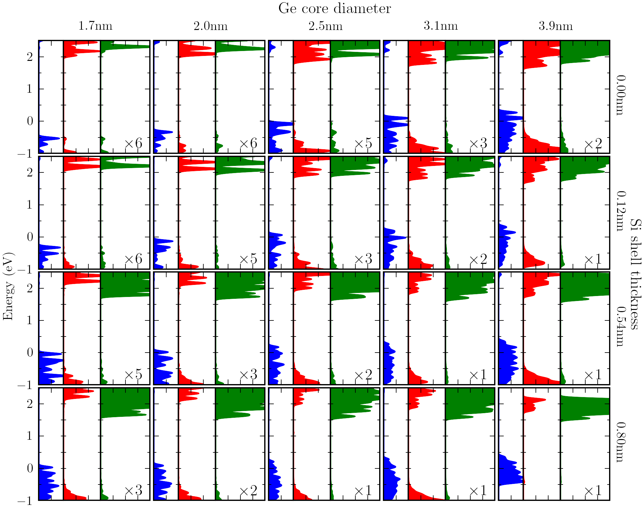
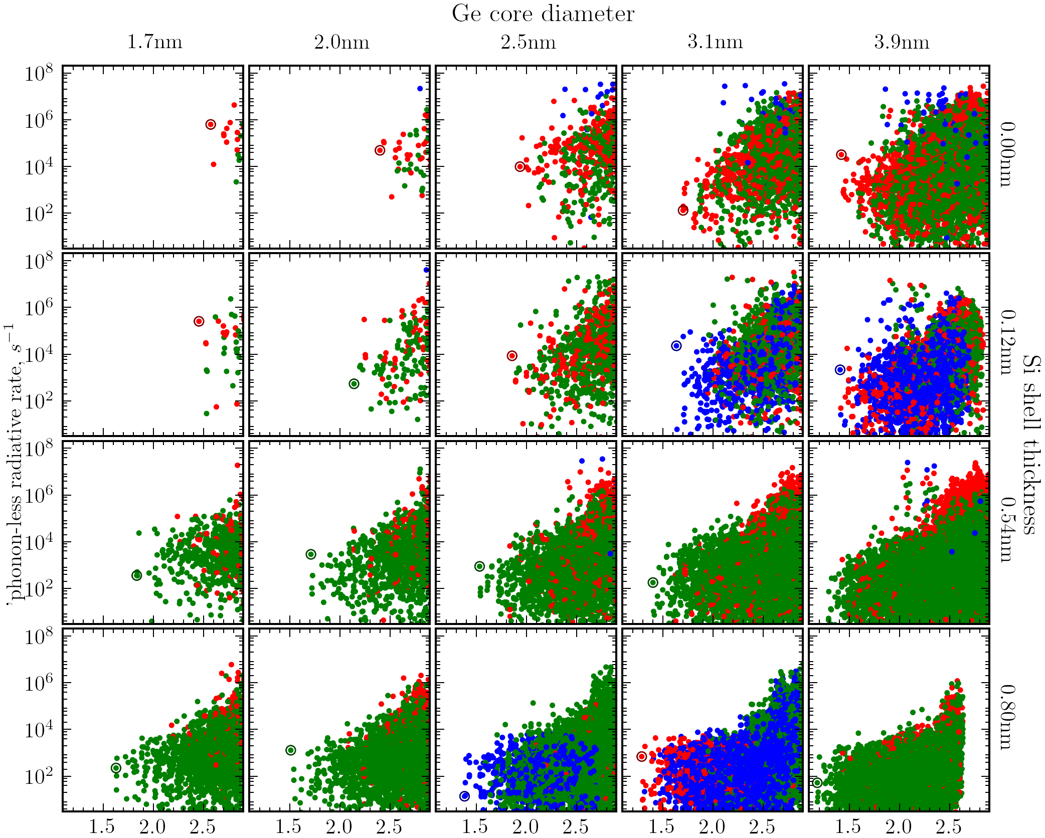
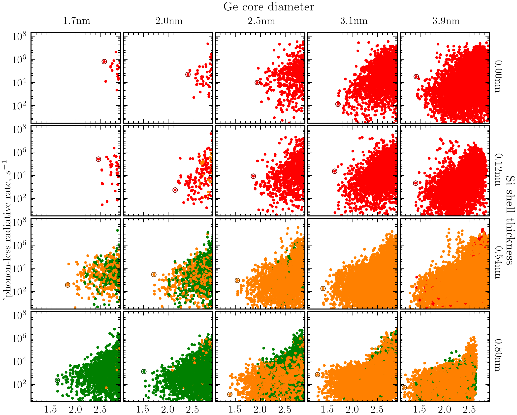
In supplementary material we present calculations for the core-shell NCs for 5 Ge core sizes of 1.7, 2.0, 2.5, 3.1 and 3.9 nm and for the Si shell thicknesses 0.00, 0.14, 0.50 and 0.80 nm. The systems are sketched in Fig. 7.
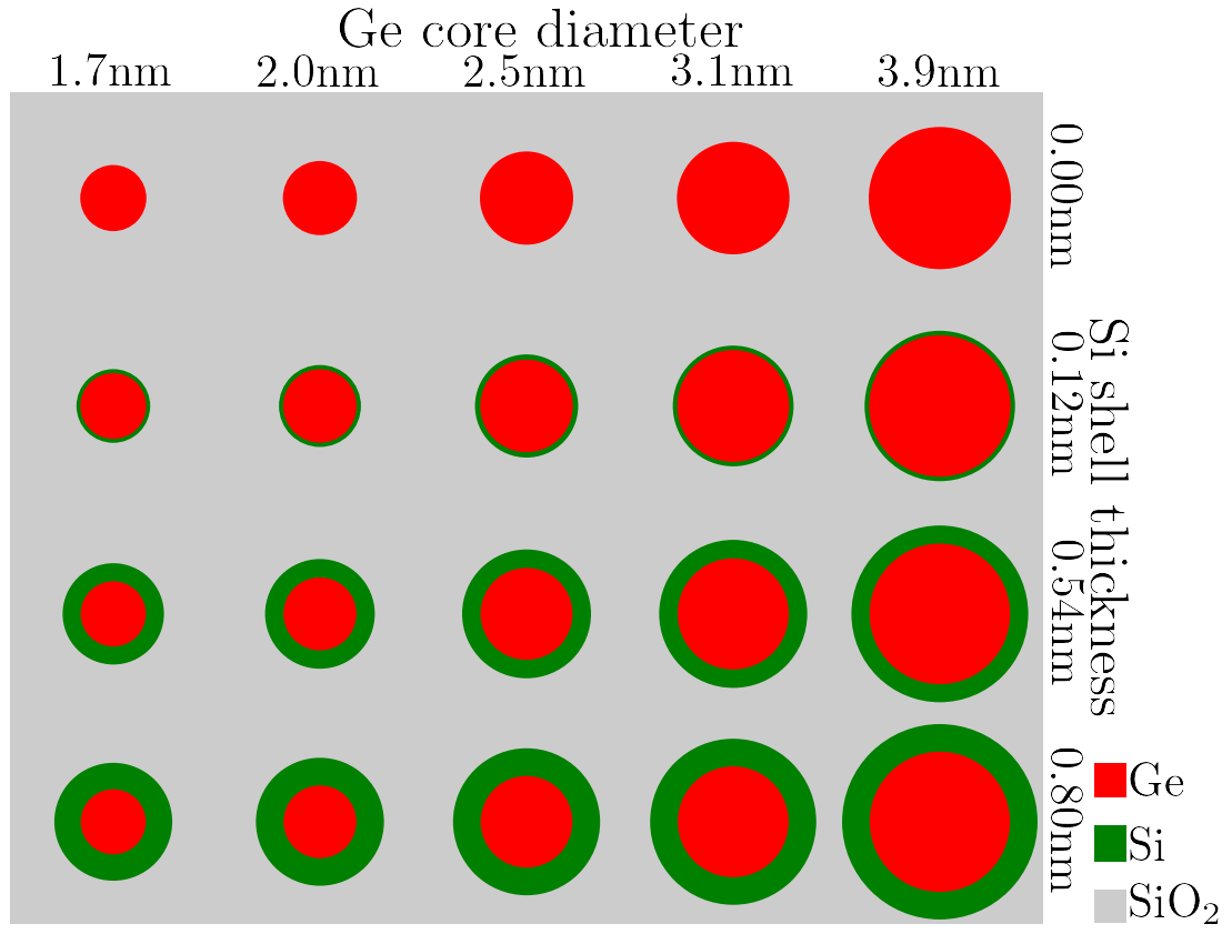
Figure 8 shows the real-space projection of the electronic density for hole and electron states. Color indicates high (red) to low (blue) DOS and the vertical gray lines denote edge of the core and shell, respectively, with the shell area in gray rectangle.
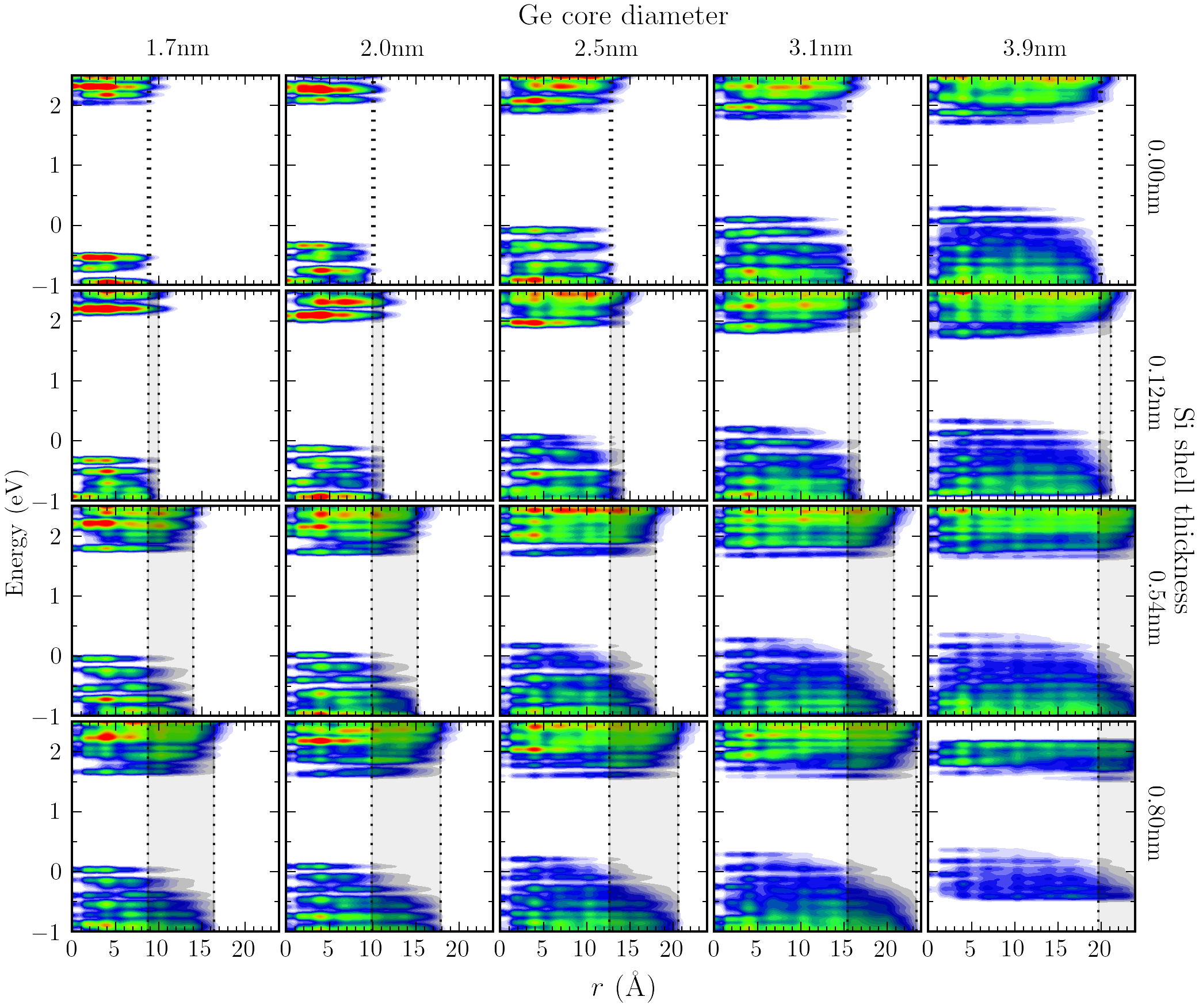
Figure 9 shows the reciprocal space projection of the electronic density for hole and electron states. Color indicates high (red) to low (blue) DOS.
In Fig. 10 we show the quantitative valley compositions obtained by integrating the reciprocals-space carrier density in the regions near , and points. To show the whole range of the DOS in all plots, we multiply the calculated DOS to the factor which is indicated in the right bottom corner of each panel.
The calculated phonon-less radiative transition rates are presented in Fig. 11. Each transition is shown by a colored dot. In order to visualize the valley structure of the electron states, the color shows the amplitude (over 40% component) in the corresponding valleys, i.e. the blue component corresponds to the electron density from over 40% in point, green component to point and red to point.
In Fig. 12 we show the real-space-colored transition rates with color signifying more than 40% localization of the electron density component in Ge core (red), Si shell (green) or delocalized equally in between (orange).
VI Tight-binding parameters
In Table 1 we present tight-binding parameters used in calculations.
| Si | Ge | “SiO2” | |
| Si(1)Ge(2) | |||
|---|---|---|---|
For the strain we use parameters from Table 3. We use simplified version of approach from Ref. Niquet et al., 2009, instead parameters we use parameters explained in Refs. Raouafi et al. (2016); Nestoklon et al. (2016)
| Si | Ge | SiGe | |