Detailed investigation of the phase transition in KxP4W8O32 and experimental arguments for a charge density wave due to hidden nesting
Abstract
Detailed structural and magnetotransport properties of the monophosphate tungsten bronze Kx(PO2)4(WO3)8 single crystals are reported. Both galvanomagnetic and thermal properties are shown to be consistent with a charge density wave electronic transition due to hidden nesting of quasi - 1D portion of the Fermi surface. We also observe the enhancement of electronic anisotropy due to reconstruction of the Fermi surface at the Peierls transition. The resistivity presents a thermal hysteresis suggesting a first order nature characteristics of a strong coupling scenario. However, other measurements such as the change of carriers density demonstrate a second order Peierls scenario with weak coupling features. We suggest that the structural transition driven by the residual strain in the K - P - O environment is responsible for the resistivity hysteresis and modifies the Fermi surface which then helps the rise to the second order Peierls instability.
pacs:
71.45.Lr, 72.15.Gd, 72.15.EbI Introduction
The low dimensional oxides have always attracted a wide attention due to their unconventional physics. The low dimensional electronic structure leads to the anisotropy of transport and thermoelectric properties and/or to electronic instabilities, including modulation of electronic or spin structure, known as Charge (or Spin) Density Waves. Low dimensionality is also an important ingredient for superconducting transition in copper oxides, and the interplay of CDW and superconductivity emerges as one of the central questions in that field Leroux et al. (2012). KxP4W8O32 belongs to the monophosphate tungsten bronzes (MPTB) family described by the general formula Ax(PO2)4(WO3)2m ( being an integer, A = Na, K, Rb, Pb). The (PO2)4(WO3)2m crystal structure is built by perovskite ReO3 type infinite layers of corner sharing WO6 octahedra connected with PO4 tetrahedra P. Roussel (2001). The regular family members possess quasi-pentagonal tunnels large enough to accommodate additional cations which results in change of their section to quasi – hexagonal Domenges et al. (1988). Depending on the nature of the tunnels, monophosphate tungsten bronzes are classified as MPTBp and MPTBh, respectively. KxP4W8O32 belongs to the MPTBp for and to MPTBh Roussel et al. (1999). It should be noted that the crystal structure of MPTB is similar to Mo4O11 Magneli phases, built of MoO6 octahedra perovskite – type layers isostructural to WO6 and MoO4 tetrahedra playing the same role in connecting Mo – O slabs as PO4 in MPTB Foury-Leylekian and Pouget (2002); Canadell et al. (1989). The MPTB low members exhibit the 2D electronic character due to 5d conduction electrons concentrated in WO6 layers Domenges et al. (1985). The electrons are donated by PO4 groups (each group donates one electron), which play the role of charge reservoir Roussel et al. (2000). Since the quantity of the PO4 groups is identical for each member, the number of conduction electrons per unit cell is independent of and equal to 4 for undoped compounds. In KxP4W8O32 the conduction electrons density is increased in comparison to its parent structure, P4W8O32 due to presence of K atoms, with valence electron transferred to conduction band. The number of electrons per unit cell is then . The undoped compounds exhibit anomalies in their resistivity associated with CDW transition due to subsequent nesting of quasi 1D portions of the Fermi Surface (FS). Such behavior has been explained in the framework of hidden nesting scenario by Canadell and Whangbo Canadell and Whangbo (1991). For the low MPTBp members, the electronic and structural transitions are observed at critical temperatures varying with Roussel et al. (2001). From X-Ray and diffuse scattering, the modulation vectors associated with the structural distortions are found to be in general agreement with the calculated nesting vector, giving support to a Peierls scenario Foury-Leylekian and Pouget (2002). On the other hand, the genuine nature of transitions in MPTBh compounds is not clarified and remains one of the most interesting open questions in this family. Some of the physical properties of KxP4W8O32 were studied over a decade ago. Only a single anomaly has been observed in this compound Roussel et al. (1997), what is in contrast to the undoped = 4, where two transitions were found Dumas et al. (2002). This anomaly was observed for varying from 0.86 to 1.94 with a maximum of = 170 K for = 1.30 Drouard et al. (1999). The anomaly was also found in the thermoelectric power (TEP) at temperatures corresponding to values of found for transition in resistivity curves. Moreover, the X-ray diffuse scattering experiments proved the existence of the long range order – structural modulation with commensurate wave vector Dusek et al. (2002); Drouard et al. (1999), unaffected by . These results, together with the existence of single electronic gapHaffner, S. et al. (2001) revealed via the infrared reflectivity measurements could be partially explained by a Peierls transition forecast by electronic structure calculations recalled aboveCanadell and Whangbo (1991). On the other hand, the fact that the - vector does not vary with , thus with the band filling was a source of controversy about the origin of the transitionDrouard et al. (1999). Furthermore, Bondarenko et al Bondarenko et al. (2004) suggested, that the relatively large anomaly observed in the specific heat at is not consistent with a CDW transition but rather indicative of structural - only character of the transition. An alternative mechanism was proposed by Dusek et al Dusek et al. (2002), explaining the transition as driven by the strain between potassium and the PO4 tetrahedra causing displacement of K, P and O atoms. The nature of transition observed in this material is then not clear. The scope of this work is to complement the information established beforehand with the new results and shed a new light on the problem of presumed CDW existence in KxP4W8O32. In a broader perspective, this sample illustrates that a weak coupling CDW can survive even if a part of the lattice is significantly distorted.
II Experimental
The single crystals with the typical size of 5 mm x 1 mm x 500 m were grown using chemical vapor transport method Giroult et al. (1982). The potassium content was determined by EDS performed with SEM FEI XL 30 FEG. High resolution X-Ray diffuse scattering was studied on a selected high quality single crystal with a size of 0.19 x 0.16 x 0.015 mm3. Scans were executed using monochromated radiation with wavelength = 0.50718 Å and beam size of 200 m x 200 m. The aim of the diffraction experiment being the measurement of a maximum of satellite reflections associated to the transition, data collection at low temperature (down to = 36 K) was accomplished with the maximum flux of the beamline but also with an attenuator for limiting possible saturation of the CCD detector by the strong main reflections. The experiment was performed both at room temperature (RT) and at = 45 K, thus far above and deep below the transition. The samples were cooled using a He gas blower. The electrical resistivity was measured using four probe method. The experiments were performed (when possible) in two directions: in the (ab) plane () and out of plane (). The contact configuration proposed by Hardy et al Hardy et al. (1997), adapted for highly anisotropic systems Warmont et al. (1998); Villard et al. (1998) was used to measure . The electrical contacts were made by welding 99,5% Al, 0,05 % Si, 25 thick wires to the sample surface. The magnetoresistance was measured with electric current applied in the (ab) plane and magnetic field maintained perpendicularly to the direction of electric field, in order to preserve a constant Lorenz force. The sample was rotated by , the angle between and c vectors. All magnetoresistance and resistivity measurements were performed using a Physical Properties Measurement System (PPMS) from Quantum Design with a 14 T magnet and equipped with horizontal rotator. The thermopower was measured in the (ab) plane, with constant thermal gradient maintained between two chromel - constantan thermocouples soldered to the sample surface with indium. The thermocouples were also used to measure thermoeletric voltage, and the experiment was performed in the PPMS with external setup. The Hall coefficient was acquired by measuring transverse voltage between two points on the sample surface in presence of longitudinal current and magnetic field applied perpendicularly to the (ab) plane. The magnetoresistance contribution was subtracted from the data. The DC magnetization was measured within a Magnetic Properties Measurement System (Squid based MPMS from Quantum Design). Oriented single crystal was weighted and fixed with paper and scotch in a polyethylene straw. Constant magnetic field was applied along (ab) plane. High value of = 1 T was used in order to achieve the finest scan resolution and extract the weak sample signal from substantially stronger background. The curve was obtained by a four probe method. The current was applied along the sample (in the (ab) plane) using Keithley 228A source, and voltage was measured by microvoltmeter. The I contacts were enhanced by welding additional AlSi wires joined together with a small drop of DuPont 6838 silver paste. The sample was kept in liquid nitrogen to ensure effective contacts cooling.
III Results and discussion
III.1 Structural analysis
The purpose of the crystallographic study is to verify the results previously obtained by Dusek et alDusek et al. (2002). In this previous study, the data was also achieved using synchrotron radiation, almost mandatory to solve the structure with such weak satellite peaks. 789 main and 409 satellite reflections with I were then collected at 110 K, thus close to the transition temperature.
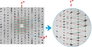
The reconstructed (h0l)∗ planes using the experimental frames collected with our single crystal at RT and 45 K (see figure 1) show unexpected extinction rules: rows running along c∗ with a periodicity of 8.9 Å alternate with rows exhibiting a periodicity of 17.8 Å. This phenomenon can be interpreted using the hypothesis of occurrence of twin domains related by a two – fold axis parallel to c; our sample exhibits then a reticular pseudo-merohedral twinning. The cell at RT was found to be monoclinic with the following cell parameters: a = 6.676(1) Å, b = 5.322(1) Å, c = 8.899(1) Å and = 100.637(2)∘. The hypothesis of a reticular pseudo-merohedral twinning has been successfully tested by a full structural refinement procedure for the RT data set.
The experiment performed at reduced temperature = 45 K revealed the existence of weak superlattice reflections. In fact, two sets of additional peaks were found; they are corresponding to satellites associated to each twin domain as shown in figure 1 and they induce the doubling of the a parameter. The observation of this two sets is a supplementary proof validating our twin hypothesis. The positions of the satellites are in agreement both with the modulation vector previously reported by Dusek et al ( = (0.5; 0; 0)) and with calculations performed by Canadell and Whangbo Canadell and Whangbo (1991), who predicted this value as associated with hidden nesting of the 1D part of the Fermi surface. The diffraction pattern lead then to the following cell parameters : a = 13.2383(6) Å, b = 5.2823(1) Å, c = 8.8511(2) Å and = 100.677(3)Å.
The data recorded at 45 K at the Cristal beamline at Soleil contain 4113 observed reflections with I , 1703 reflections with (i.e. satellites) and 2410 reflections with (i.e. main); indices are referring to the unit cell above. The data set is then globally 3.4 times larger than the one collected by Dusek et al and we are observing 4.15 times more satellite reflections directly related to the transition. Note that the data collection was performed deep below the transition temperature to achieve the largest possible enhancement of the satellite reflections. However, let us notice that our sample exhibits a reticular pseudo-merohedral twinning; the two domains are related by a mirror perpendicular to a. The main reflections of both domains are fully or partly overlapped and the integration process requires additional corrections; the intensity of the main reflections is then expected to be less reliable than the fully separated satellites (see figure 1).
The refinement procedure was achieved using Jana2006 Petříček et al. (2014) in the 3-dimensional supercell with the space group following the analysis of Dusek et al. The structure is fully described by 4 W, 2 P, 2 K and 16 O atoms. The atomic displacement parameters (ADP) were considered isotropic for O atoms and anisotropic in the other cases. Atoms related by inversion center in the centrosymmetic approximation are restricted to have the same ADP. The occupancy of the two K atoms is refined; they exhibit a partial occupancy of 0.291(4) and 0.279(4) leading to the chemical composition K1.14(2)P4W8O32, close to the expected formula. The final agreement factors, with 109 refined parameters, are 6.97% for the 4113 reflections, 6.78% for the 2410 reflections with and 8.05% for the 1703 reflections with . Atomic parameters of this refinement are given in table 1 and atomic distances in table 2.
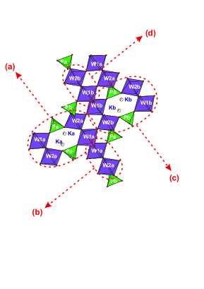
The structural results obtained at 45 K are compared with the analysis performed at room temperature (RT). The deviations between the atomic positions at 45 K and RT are reported in the table 1. The maximum atomic displacements observed for the O, K, P and W atoms are 0.19, 0.054, 0.111 and 0.034 Å respectively (see table 1). These moderate values evidenced for W were already reported by Dusek et al Dusek et al. (2002); they did not induce any significant change in the W-W boundaries. The figure 3 shows the main modifications observed at 45 K for the cation-oxygen distances corresponding to the structure zones indicated in figure 2. The superstructure observed at 45 K does not induce the large distortions in the WO or PO bounding scheme (see mainly figure 3 b and c). The strongest effect is related to the geometry of the hexagonal windows (see figure 3 a and d). A dilatation of the cavities is observed in the direction of the Pa-Pa segment and a contraction in the perpendicular direction.
| atom | occu | x | y | z | Ueq (Å2) | |
|---|---|---|---|---|---|---|
| pation | (Å) | |||||
| W1a | 1 | -0.06936(3) | -0.25383(9) | 0.58862(5) | 0.00054(6) | 0.021 |
| W1b | 1 | -0.43044(3) | 0.25641(10) | -0.58770(5) | 0.00054(6) | 0.034 |
| W2a | 1 | -0.21793(4) | 0.24434(9) | 0.74920(5) | 0.00052(6) | 0.030 |
| W2b | 1 | -0.28222(3) | -0.24711(8) | -0.74907(5) | 0.00052(6) | 0.016 |
| Pb | 1 | 0.3545(2) | 0.2398(7) | 0.1290(4) | 0.0015(3) | 0.054 |
| Pa | 1 | -0.8546(2) | -0.2434(7) | -0.1298(4) | 0.0015(3) | 0.036 |
| O1a | 1 | 0.3664(6) | 0.2387(19) | -0.0386(8) | 0.0024(5) | 0.066 |
| O1b | 1 | -0.8691(6) | -0.2532(18) | 0.0379(9) | 0.0024(5) | 0.022 |
| O2a | 1 | 0.3055(6) | -0.0143(15) | 0.1582(10) | 0.0025(5) | 0.179 |
| O2b | 1 | -0.8092(7) | -0.0002(15) | -0.1660(10) | 0.0025(5) | 0.155 |
| O3a | 1 | -0.3225(6) | 0.2358(16) | 0.5760(9) | 0.0033(6) | 0.115 |
| O3b | 1 | -0.1858(6) | -0.2418(16) | -0.5767(11) | 0.0033(6) | 0.049 |
| O4a | 1 | 0.4625(6) | 0.266(2) | 0.2222(9) | 0.0030(5) | 0.131 |
| O4b | 1 | -0.9631(6) | -0.256(2) | -0.2218(10) | 0.0030(5) | 0.010 |
| O5a | 1 | 0.0112(6) | -0.0176(12) | 0.4944(9) | 0.0007(5) | 0.190 |
| O5b | 1 | -0.4997(5) | 0.0081(12) | -0.5041(8) | 0.0007(5) | 0.057 |
| O6a | 1 | -0.1439(6) | 0.4945(14) | 0.6855(9) | 0.0015(5) | 0.046 |
| O6b | 1 | -0.3518(6) | -0.5164(14) | -0.6898(9) | 0.0015(5) | 0.145 |
| O7a | 1 | -0.1364(7) | 0.0030(15) | 0.6903(10) | 0.0016(5) | 0.057 |
| O7b | 1 | -0.3651(7) | -0.0200(15) | -0.6833(10) | 0.0016(5) | 0.129 |
| O8a | 1 | 0.2976(6) | 0.4692(15) | 0.1667(10) | 0.0030(5) | 0.104 |
| O8b | 1 | -0.7880(6) | -0.4643(15) | -0.1587(9) | 0.0030(5) | 0.182 |
| Ka | 0.29(1) | -1.0697(7) | -0.2354(18) | -0.0011(10) | 0.0042(10) | 0.111 |
| Kb | 0.28(1) | 0.5706(7) | 0.246(2) | 0.0027(11) | 0.0042(10) | 0.099 |
| boundary | d (Å) | boundary | d (Å) | boundary | d (Å) |
|---|---|---|---|---|---|
| W1a-O3bi | 1.920(8) | W1b-O3av | 1.840(7) | W2a-O1bix | 2.018(7) |
| W1a-O4bii | 1.979(8) | W1b-O4avi | 1.990(7) | W2a-O2ax | 1.999(9) |
| W1a-O5a | 1.929(8) | W1b-O5b | 1.833(7) | W2a-O3a | 1.866(7) |
| W1a-O5aiii | 1.812(7) | W1b-O5bvii | 1.887(7) | W2a-O6a | 1.797(8) |
| W1a-O6aiv | 1.947(8) | W1b-O6bviii | 1.921(8) | W2a-O7a | 1.808(9) |
| W1a-O7a | 1.932(9) | W1b-O7b | 1.967(9) | W2a-O8aiii | 2.018(8) |
| W2b-O1axi | 2.000(7) | Pa-O1b | 1.532(9) | Pb-O1a | 1.521(8) |
| W2b-O2bxii | 2.038(9) | Pa-O2b | 1.478(9) | Pb-O2a | 1.533(9) |
| W2b-O3b | 1.799(8) | Pa-O4b | 1.517(8) | Pb-O4a | 1.520(8) |
| W2b-O6b | 1.824(8) | Pa-O8b | 1.513(9) | Pb-O8a | 1.496(9) |
| W2b-O7b | 1.794(9) | ||||
| W2b-O8bvii | 2.011(8) | ||||
| Ka-O1bxiii | 2.616(12) | Kb-O1a | 2.660(12) | ||
| Ka-O1bxiv | 2.854(13) | Kb-O1axviii | 2.807(14) | ||
| Ka-O1bxv | 2.675(13) | Kb-O1axix | 2.734(14) | ||
| Ka-O2axvi | 3.499(12) | Kb-O2axix | 2.681(14) | ||
| Ka-O2bxiv | 2.755(13) | Kb-O2bxx | 3.489(12) | ||
| Ka-O4bxiii | 2.615(14) | Kb-O4a | 2.619(14) | ||
| Ka-O4bxiv | 3.366(14) | Kb-O4axviii | 3.201(14) | ||
| Ka-O4bxv | 3.190(13) | Kb-O4axix | 3.375(14) | ||
| Ka-O6axvii | 3.112(12) | Kb-O6b? | 3.000(12) | ||
| Ka-O7av | 2.989(12) | Kb-O7bii | 3.089(12) | ||
| Ka-O8axvi | 3.284(12) | Kb-O8axviii | 2.899(14) | ||
| Ka-O8bxv | 2.931(13) | Kb-O8bxx | 3.154(12) |
The paper written by Dusek et al Dusek et al. (2002) provides a comparison between the average structure and the superstructure both calculated from the data collected at 110 K. Our present description details the differences observed between the structure of the fundamental state at room temperature and the structure at 45 K deep below the transition. The large number of observed independent satellite reflections (4.5 times more than in the previous study Dusek et al. (2002)) leads to a high degree of confidence in our result and very low standard deviations. This last point is very important since the differences observed above and below the transition are very weak in term of atomic positions (see table 1) and even slighter in term of distances (see figure 3). The obtained results clearly validate the conclusions drawn by Dusek et al Dusek et al. (2002): the main changes at 45 K are occurring for the phosphorus and potassium environment as evidence by the variations of the K-O and P-O distances. However for us, such effect does not contradict the possibility of CDW formation since weak but significant deviations ( 0.01 to 0.02 Å) are also observed for W-W and W-O distances.


III.2 Physical properties
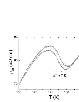
The typical in - plane resistivity vs. temperature curves, measured for different , are shown in fig. 4.
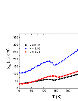
As previously reportedDumas et al. (2002); Drouard, S. et al. (2000), a clear anomaly is observed in the 100 - 150 K range at a temperature , which depends on the potassium value. Additionally, a small thermal hysteresis is observed at the transition. To ensure, if this effect is truly intrinsic to the sample and is not an artifact caused by insufficient thermalisation, we have repeated the scan with heating/cooling rate as low as 0.05 K/min. As a result, we have found the reproducible hysteresis, with a very similar width of K for = 1.21 (shown in fig. 6) and = 1.10 and, a smaller one ( K) for = 0.93.
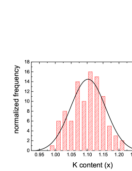
To go deeper insight into this anomaly, we have performed additional sample characterizations and analyzed in details the distribution of potassium content in the crystals. The idea behind is that any departure from a very precise stoichiometry could result in a broadening of the transition, as it is well known in high Tc cuprates for instanceShi et al. (1989). The performed EDS scans reveal, that the samples composition is not perfectly homogeneous at the sample scale. The K distribution for the = 1.10 crystal is shown in fig. 5. We find, that it can be described by the Gaussian decay with and FWHM = 0.11.
Considering the dependence Drouard, S. et al. (2000), one can expect a broadening of corresponding to the obtained distribution width. Note that strictly, that although stands in agreement with the hysteresis size only a broadening is expected by such a effect. One could consider the scenario of the current percolation in the preferential zones, which undergo the transition at various temperatures as an explanation of the macroscopic hysteresis, however this picture would lead to the deviation from the Ohmic behavior, which is not observed in our samples. Therefore, we find this mechanism irrelevant to explain the hysteretic manner of resistivity. Note, that the existence of hysteresis can be a fingerprint of a first-order transition, a priori unexpected in the framework of Peierls-Frohlich theory which is a continuous second order transition Grüner (1988). The Ginzburg Landau approach predicts the first order character of a lock - in transition separating an incommensurate state at high temperature and a commensurate state McMillan (1975). Such effects observed in various CDW materials as TaSe2Moncton et al. (1977) or K0.3MoO3Fleming et al. (1985). We find this case unlikely here, since neither transport or structural properties reveal any sign of an incommensurate CDW at higher temperatures. However it shall be noted that the first order transitions towards CDW has been reported in Lu5Rh4Si10 Lue et al. (2002), Lu5Ir4Si10 Becker et al. (3 15); Leroux et al. (2 19); Jung et al. (2003) without any signatures of CDW phase at higher temperatures.
The anisotropy in electronic properties, expected in a quasi 2D system is inferred by measurements of the out of plane resistivity (fig. 7).
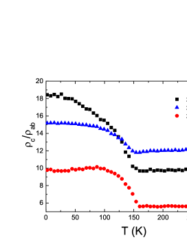
This latter shows a typical metallic behavior consistent with a coherent scattering perpendicular to the most conducting planes and an anomaly at . The anisotropy of resistivity varies from 6 to 12 at room temperature. is strictly constant down to , but remarkably grows from to low temperature. This indicates a strong increase of the transport anisotropy. The reinforcement of anisotropy has been noted in materials with CDW as NbSe2LeBlanc and Nader (2010), albeit without quantitative analysis. The constant electronic anisotropy for is consistent with a simple metallic state. For , the strong change indicates that this anisotropy changes likely due to a Fermi surface reconstruction. It shall also be noticed, that the temperature variation of is very similar to the thermal dependence of a Peierls gap. From this observation, at least we can propose that its main origin is not from the change of electronic mobility of carriers, but rather from an anisotropic change of carriers density at .
Magnetotransport measurements show a positive, metallic-like, magnetoresistance (MR), which increases significantly below , as shown in fig. 8.
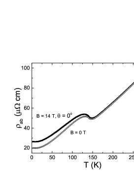
The MR follows a cosine law, reaching maximum for , and is almost zero when lies in the (ab) plane. The regime followed by the magnetoresistance is a typical signature of cylindrical, quasi 2D topology of the Fermi surface Pippard (1989). The MR can be discussed in the framework of the Kohler’s rule, predicting that all the Kohler’s plots:
| (1) |
(where is the cyclotron frequency and is the scattering time) follow the same curve, if is identical for all carriers, and constant in all parts of Fermi surface McKenzie et al. (1998). In fig 9, we show the Kohler plot for the = 1.20 sample.
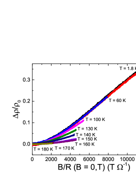
One can notice that all the curves for temperatures above 158 K fall into one line. When decreasing further the temperature, the Kohlers’s rule is violated down to 60 K, where it is again satisfied. Different causes can lead to a breakdown of Kohler’s ruleMcKenzie et al. (1998). One possibility is the formation of a density wave at a critical temperature and of a concomitant change of electronic structure, as observed in other materials with Peierls instability such as NbSe3 Yasuzuka et al. (2005). In this case, the change is expected to be significant down to roughly where the gap starts to be fully open Grüner (1988). This is consistent with our observations.
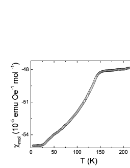
The magnetic properties of a large oriented single crystal K1.16P4W8O32 with mass = 0.0744 g have been measured. The background magnetization due to the sample holder was measured and carefully removed. Then the parasitic Curie - Weiss contribution () due to paramagnetic impurities was quantified and subtracted from the data. The obtained magnetic susceptibility is shown in the figure 10. Above , is almost temperature independent, while for one observes a notable drop of magnetic susceptibility, reminiscent to the decrease of due to the gap opening and CDW condensation of free electronic carriers reported in known CDW materials as Tl0.3MoO3 Collins et al. (1985), Mo4O11 Schlenker et al. (1986), or in undoped MPTBp = 4 Teweldemedhin et al. (1992).
To analyse the data, one has to consider the following contributions in a metallic-like sample:
| (2) |
The - the ion core diamagnetism, and – Van Vleck paramagnetism of ions, were assumed to be constant with temperature. From the remaining ingredients: , the Pauli paramagnetism of conduction electrons, and Landau diamagnetism of carriers () we have deduced the number of condensed electrons as a function of temperature, shown in fig. 11. The maximum corresponds to 15% of the electronic density calculated from chemical formula ( = 8.16 ).
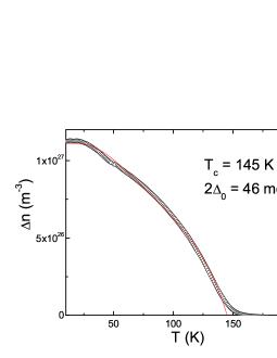
In a BCS - Peierls description of the CDW transition, the number of condensed electrons follows the temperature variationKhasanov et al. (2008):
| (3) |
with the electronic gap:
| (4) |
where is the electronic gap at = 0 K. Here, we find a good fit with a BCS-mean weak coupling expression. A slightly better fit can be proposed when removing the low temperature part ( K) where the raw data is affected by the parasitic Curie Weiss contribution. However, since this does not change significantly the fitting parameters, we prefer to show the fit on all the K part. We have found the electronic gap 2 = 46 meV for = 1.15 , which converges with the value predicted by mean – free model in limit of the the weak electron – phonon coupling 2 3.52 44.6 meV. Here, we have to mention the work of Haffner et al Haffner, S. et al. (2001) who have measured the infrared absorption of K1.30P4W8O32. They report at low temperature absorption peaks which were tentatively attributed to single-particle excitations across a gap. In this framework, a value 43 meV can be deduced. It is worth noting that this value compares extremely well with our magnetization data and this indicates that condensed carriers are effectively at the origin of these absorption peaks as proposed by Haffner et al.
To go deeper insight into the change of carrier density upon the transition, we have conducted the study of thermopower with various potassium concentrations. The temperature dependence of Seebeck coefficient for different values of is shown in fig. 12.
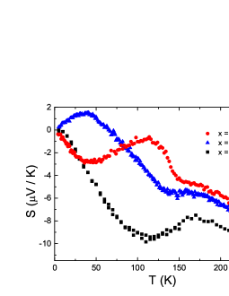
All present a transition between two metallic regimes, with linear curves, at low and high temperatures. In the transition region, depending on , the transition is associated to an increase of ( = 0.93), a decrease of ( = 1.21), or for the intermediate doping ( = 1.16), a constant value of . The thermopower even turns positive at low temperature for = 1.16. The above described behaviors are in good agreement with the results reported previously Drouard, S. et al. (2000); Roussel et al. (1997). The maximum in close to = 0, indicates enhancement of the hole influence for = 0.93. On the other hand, electrons remain dominant carriers in = 1.21 compound. Roussel et al Roussel et al. (1997) suggested, that strong change of slope and existence of an extremum, either in positive or negative direction might result from Peierls transition with high – mobility carriers left in the pockets remaining after imperfect nesting of the Fermi surface. To follow the thermal evolution of the effective electronic density containing both the electrons and holes contributions (with opposite signs), we have applied the semi - classical 3D model of quasi - free electrons Pallecchi et al. (2010):
| (5) |
The carrier density at high temperature () and the loss of carriers due to the transition () were estimated from the linear parts of at high and low temperatures respectively, with an assumption, that the in - plane effective mass and is constant with T both for electrons and holes. We have assumed the scattering factor , corresponding to scattering with acoustic phonons. The obtained - effective electronic density for is for each sample (see table 3) reasonably close to the values calculated from the chemical formula (). For = 1.16, one can compare the concentration of condensed carriers deduced from both the magnetic measurements and the Seebeck measurements. We find respectively and , that is in rather good agreement. This shows, that the used model, despite of its roughness can serve as an useful guide in the estimation of carriers density in quasi 2D metals.
| K content | [1027 m-3] | [1027 m-3] | [%] |
|---|---|---|---|
| 0.93 | 7.88 | 2.72 | 22.20 |
| 1.10 | 8.16 | 2.26 | 12.13 |
| 1.16 | 8.28 | 2.35 | 34.16 |
| 1.21 | 8.34 | 4.70 | 8.67 |
The found in compounds with visible hole contribution are notably higher than one found for = 1.21, where the electrons are dominant in whole temperature range. This effect can be explained as caused both by condensation of electrons, thus their removal from the conduction band and the increase of role of light holes, which contribute to neff with sign opposite to electrons.
The investigation of the existence of CDW in low dimensional material must not omit the search for non - Ohmic DC transport. The evidence of Fröhlich transport has already been reported in a number of quasi 1D materials as NbSe3 Monceau et al. (1976), K0.3MoO3Dumas et al. (1983); Forró et al. (1986) or Tl0.3MoO3 Collins et al. (1985), while the attempts to observe CDW sliding in quasi 2D materials were unsuccessful even in powerful electric fields DiSalvo and Fleming (1980) with exception only to single compound, DyTe3 Sinchenko et al. (2012). The difficulty with the study of this effect arises both from notably stronger pinning observed in 2D systems and from metallicity which remains in 2D materials after imperfect nesting of the Fermi surface, which obstructs reaching strong electric fields. We have performed the measurement of the curve in K1.15P4W8O32 sample cooled in liquid nitrogen applying DC current up to = 6 A, reaching maximum electric field of = 121 mV/cm. No break of linearity in DC transport was found in this temperature range. We also emphasize, that while the CDW nesting vector doubles the cell periodicity, the depinning energy can be significantly increased by the commensurability term Lee and Rice (1979); Lee et al. (1974); Dumas and Feinberg (1986) which can even prevail over the impurity pinning as in quasi 1D (2,5(OCH3)2 DCNQI)2Li Tomić et al. (1997). Note, that the maximum we have reached is a factor of 5 smaller than the minimum threshold field in DyTe3 which rises further at temperatures far below and the commensurability term in KxP4W8O32 is expected to raise the pinning potential to the values comparable to the electronic gap. We suggest, that the lack of observed non-linearity is caused by strong pinning arising both from commensurate nature of the modulation and from the 2D electronic character of the tested material. Therefore, the lack of non-linearity in DC transport can not contradict the CDW scenario in KxP4W8O32.
III.3 Discussion
The nature of the transitions observed in KxP4W8O32 was a subject of an intensive dispute. Drouard et. al Drouard et al. (1999) remarked, that the modulation vector should significantly vary with , while for each one observes the identical = 0.50 a∗ modulation vector. On the contrary, the band structure calculations performed by Canadell et alCanadell and Whangbo (1991) predict, that the modulation vector associated with hidden nesting of quasi 1D part of the KxP4W8O32 Fermi surface varies from 0.47 a∗ to 0.50 a∗ for = 0.8 and = 3.5 respectively and this deviation is far from significant. Bondarenko et alBondarenko et al. (2004) concluded, that the large (in comparison to the undoped = 4) change in the specific heat due to transition observed at indicates that the transition is essentially structural and not a simple CDW transition. Nevertheless, we find the comparison between ( is the number of electrons per formula unit and = 8.31 J mol-1 K-1 is the gas constant) in KxP4W8O32 and corresponding quantities in ’well established’ CDW materials misguiding. Considering both electrons donated by P groups and K atoms in the tunnels, the value of p should denote 5.07, 5.30, and 5.45 for = 1.07, = 1.30 and = 1.45 respectively, instead of values slightly larger than unity considered by Bondarenko et al. Then, we find that for KxP4W8O32 should vary between 0.27 and 0.47 for = 1.07 and = 1.45 respectively, which is finally smaller than the values found in examples of known CDW materials K0.3MoO3 (0.53), KMo6O17 (0.40) or Mo4O11 (0.78), recalled by Bondarenko et al. Then, the argument that is too large to be attributed to a single CDW transition appears not very strong. Dusek et alDusek et al. (2002) suggested, that the transition is driven by atomic displacements due to strain induced between K atoms and the PO4 tetrahedra instead of the CDW formation. We agree, that this mechanism would produce a change in the electronic band structure, but its effect is not essential to explain the physical properties showing modification of the Fermi surface accompanied with carrier condensation. The small hysteresis observed in resistivity is an indicative of a first - order transition, suggesting the strong lattice component of the observed anomaly. Such scenario is expected in a strong coupling approach McMillan (1977). On the other hand, this model predicts the electronic gap to be substantially larger than the weak coupling value of 2 3.52 Kwok et al. (1990); Smontara et al. (1992). This is not relevant in KxP4W8O32, since our results show the excellent agreement between the measured electronic gap and the weak coupling prediction. In the strong coupling scenario, at , the short order fluctuations are still preserved leading to diffuse scattering in the vicinity of superlattice reflections observed below Rossnagel (2011) which is not visible in our sample even with synchrotron radiation. Another interesting point is also the weakness of structural distortion in the W-O assembly (displacements in W-O and W-W distances are 0.01 to 0.02 Å) associated with the CDW formation in MPTBFoury-Leylekian et al. (2002); P. Roussel (2001), which does not corroborate with the requirement of large distortions in strong coupling mode. The BCS character of condensed electronic density and electronic gap are strong arguments for a genuine second order nature of the electronic part of the transition. Note, that the hysteresis is not visible in magnetic susceptibility. Then, it is reasonable to assume, that the hysteretic behavior of resistivity likely originates from the structural distortion in K-P-O environment which produces an additional effect on the scattering term. In this picture, if one considers the residual strain between K atoms and PO4 tetrahedra as a main driving force of the structural transition in KxP4W8O32, the Peierls instability can be seen as a by - product of the structure modification. The evolution of a band structure upon the transition allows the nesting of a 1D fragment of the Fermi surface with a preferential wavevector , independent of and overcome the suppression of the CDW Ppuget and Comes (1989) due to the disorder caused by inhomogeneous potassium distribution. Then, it is favorable to maintain this commensurate value unchanged with K content to preserve the optimal nesting conditions. This sort of resonance of CDW and the underlying lattice leading to existence of one privileged modulation vector can partially explain the lack of subsequent nesting of remaining Fermi surface parts as predicted by Canadell and Whangbo Canadell and Whangbo (1991) or observed in undoped P4W8O32 Dumas et al. (2002).
IV conclusions
In this article, we report a full set of experimental data on KxP4W8O32,
including new high resolution X-Ray data, magnetic susceptibility,
and detailed chemical characterization to focus on the nature of
the transition observed at . We conclude, that the anomalies observed in physical properties of Kx(PO2)4(WO3)8 are associated with condensation of
around 15 % of the total number of carriers and the hidden nesting of the quasi 1D portion of the Fermi Surface. We also find the enhancement of transport properties anisotropy upon the FS modification. Despite the resistivity hysteresis, we have provided the strong evidence for the weak coupling Peierls scenario. We propose that the thermal hysteresis does not arise from a first order characteristics, but from scattering due to residual strains around the structural transition, which also modifies the Fermi surface and enables the second order charge density wave instability.
Acknowledgements.
Financial support by the French National Research Agency ODACE ANR-Project number 2011-BS04-004-01 is gratefully acknowledged.References
- Leroux et al. (2012) M. Leroux, M. Le Tacon, M. Calandra, L. Cario, M.-A. Méasson, P. Diener, E. Borrissenko, A. Bosak, and P. Rodière, Phys. Rev. B 86, 155125 (2012).
- P. Roussel (2001) P. L. P. Roussel, O. Pérez, Acta Cryst. B 57, 603 (2001).
- Domenges et al. (1988) B. Domenges, M. Hervieu, B. Raveau, and M. O’Keeffe, Journal of Solid State Chemistry 72, 155 (1988).
- Roussel et al. (1999) P. Roussel, D. Groult, A. Maignan, and P. Labbé, Chemistry of Materials 11, 2049 (1999).
- Foury-Leylekian and Pouget (2002) P. Foury-Leylekian and J.-P. Pouget, Solid State Sciences 4, 387 (2002).
- Canadell et al. (1989) E. Canadell, M. H. Whangbo, C. Schlenker, and C. Escribe-Filippini, Inorganic Chemistry 28, 1466 (1989).
- Domenges et al. (1985) B. Domenges, N. McGuire, and M. O’Keeffe, Journal of Solid State Chemistry 56, 94 (1985).
- Roussel et al. (2000) P. Roussel, P. Labbé, H. Leligny, D. Groult, P. Foury-Leylekian, and J. P. Pouget, Phys. Rev. B 62, 176 (2000).
- Canadell and Whangbo (1991) E. Canadell and M.-H. Whangbo, Phys. Rev. B 43, 1894 (1991).
- Roussel et al. (2001) P. Roussel, O. Pérez, and P. Labbé, Acta Crystallographica Section B 57, 603 (2001).
- Roussel et al. (1997) P. Roussel, D. Groult, C. Hess, P. Labbe, and C. Schlenker, Journal of Physics: Condensed Matter 9, 7081 (1997).
- Dumas et al. (2002) J. Dumas, U. Beierlein, S. Drouard, and C. Schlenker, Solid State Sciences 4, 379 (2002).
- Drouard et al. (1999) S. Drouard, P. Foury, P. Roussel, D. Groult, J. Dumas, J. Pouget, and C. Schlenker, Synthetic Metals 103, 2636 (1999), international Conference on Science and Technology of Synthetic Metals.
- Dusek et al. (2002) M. Dusek, J. Ludecke, and S. van Smaalen, J. Mater. Chem. 12, 1408 (2002).
- Haffner, S. et al. (2001) Haffner, S., Dressel, M., Groult, D., and Schlenker, C., Eur. Phys. J. B 24, 167 (2001).
- Bondarenko et al. (2004) V. Bondarenko, J. Brill, J. Dumas, and C. Schlenker, Solid State Communications 129, 211 (2004).
- Giroult et al. (1982) J. Giroult, M. Goreaud, P. Labbe, and B. Raveau, Journal of Solid State Chemistry 44, 407 (1982).
- Hardy et al. (1997) V. Hardy, A. Maignan, C. Martin, F. Warmont, and J. Provost, Phys. Rev. B 56, 130 (1997).
- Warmont et al. (1998) F. Warmont, V. Hardy, J. Provost, D. Grebille, and C. Simon, Phys. Rev. B 57, 7485 (1998).
- Villard et al. (1998) G. Villard, A. Daignere, A. Maignan, and A. Ruyter, Journal of Applied Physics 84, 5080 (1998).
- Petříček et al. (2014) V. Petříček, M. Dušek, and L. Palatinus, Zeitschrift für Kristallographie - Crystalline Materials 229, 345 (2014).
- Drouard, S. et al. (2000) Drouard, S., Groult, D., Dumas, J., Buder, R., and Schlenker, C., Eur. Phys. J. B 16, 593 (2000).
- Shi et al. (1989) D. Shi, M. S. Boley, M. Patel, R. K. Kalia, and P. Vashishta, Journal of Applied Physics 66, 2074 (1989).
- Grüner (1988) G. Grüner, Rev. Mod. Phys. 60, 1129 (1988).
- McMillan (1975) W. L. McMillan, Phys. Rev. B 12, 1187 (1975).
- Moncton et al. (1977) D. E. Moncton, J. D. Axe, and F. J. DiSalvo, Phys. Rev. B 16, 801 (1977).
- Fleming et al. (1985) R. M. Fleming, L. F. Schneemeyer, and D. E. Moncton, Phys. Rev. B 31, 899 (1985).
- Lue et al. (2002) C. S. Lue, Y.-K. Kuo, F. H. Hsu, H. H. Li, H. D. Yang, P. S. Fodor, and L. E. Wenger, Physical Review B 66, 033101 (2002).
- Becker et al. (3 15) B. Becker, N. G. Patil, S. Ramakrishnan, A. A. Menovsky, G. J. Nieuwenhuys, J. A. Mydosh, M. Kohgi, and K. Iwasa, Physical Review B 59, 7266 (1999-03-15).
- Leroux et al. (2 19) M. Leroux, P. Rodière, and C. Opagiste, Journal of Superconductivity and Novel Magnetism 26, 1669 (2012-12-19).
- Jung et al. (2003) M. H. Jung, H. C. Kim, A. Migliori, F. Galli, and J. A. Mydosh, Physical Review B 68, 132102 (2003).
- LeBlanc and Nader (2010) A. LeBlanc and A. Nader, Solid State Communications 150, 1346 (2010).
- Pippard (1989) A. Pippard, Magnetoresistance in Metals, Cambridge studies in low temperature physics (Cambridge University Press, 1989).
- McKenzie et al. (1998) R. H. McKenzie, J. S. Qualls, S. Y. Han, and J. S. Brooks, Phys. Rev. B 57, 11854 (1998).
- Yasuzuka et al. (2005) S. Yasuzuka, K. Yamaya, Y. Okajima, S. Tanda, N. Takeshita, H. Mitamura, T. Nakanishi, and N. Môri, Journal of the Physical Society of Japan 74, 1787 (2005).
- Collins et al. (1985) B. Collins, K. Ramanujachary, M. Greenblatt, and J. Waszczak, Solid State Communications 56, 1023 (1985).
- Schlenker et al. (1986) C. Schlenker, S. Parkin, and H. Guyot, Journal of Magnetism and Magnetic Materials 54–57, Part 3, 1313 (1986).
- Teweldemedhin et al. (1992) Z. S. Teweldemedhin, K. V. Ramanujachary, and M. Greenblatt, Phys. Rev. B 46, 7897 (1992).
- Khasanov et al. (2008) R. Khasanov, P. W. Klamut, A. Shengelaya, Z. Bukowski, I. M. Savić, C. Baines, and H. Keller, Phys. Rev. B 78, 014502 (2008).
- Pallecchi et al. (2010) I. Pallecchi, M. Codda, E. Galleani d’Agliano, D. Marré, A. D. Caviglia, N. Reyren, S. Gariglio, and J.-M. Triscone, Phys. Rev. B 81, 085414 (2010).
- Monceau et al. (1976) P. Monceau, N. P. Ong, A. M. Portis, A. Meerschaut, and J. Rouxel, Phys. Rev. Lett. 37, 602 (1976).
- Dumas et al. (1983) J. Dumas, C. Schlenker, J. Marcus, and R. Buder, Phys. Rev. Lett. 50, 757 (1983).
- Forró et al. (1986) L. Forró, J. R. Cooper, A. Jánossy, and K. Kamarás, Phys. Rev. B 34, 9047 (1986).
- DiSalvo and Fleming (1980) F. DiSalvo and R. Fleming, Solid State Communications 35, 685 (1980).
- Sinchenko et al. (2012) A. A. Sinchenko, P. Lejay, and P. Monceau, Phys. Rev. B 85, 241104 (2012).
- Lee and Rice (1979) P. A. Lee and T. M. Rice, Phys. Rev. B 19, 3970 (1979).
- Lee et al. (1974) P. Lee, T. Rice, and P. Anderson, Solid State Communications 14, 703 (1974).
- Dumas and Feinberg (1986) J. Dumas and D. Feinberg, EPL (Europhysics Letters) 2, 555 (1986).
- Tomić et al. (1997) S. Tomić, N. Biškup, M. Pinterić, J. U. von Schütz, H. Schmitt, and R. Moret, EPL (Europhysics Letters) 38, 219 (1997).
- McMillan (1977) W. L. McMillan, Physical Review B 16, 643 (1977).
- Kwok et al. (1990) R. S. Kwok, G. Gruner, and S. E. Brown, Physical Review Letters 65, 365 (1990).
- Smontara et al. (1992) A. Smontara, K. Biljakovic, J. Mazuer, P. Monceau, and F. Levy, Journal of Physics: Condensed Matter 4, 3273 (1992).
- Rossnagel (2011) K. Rossnagel, Journal of Physics: Condensed Matter 23, 213001 (2011).
- Foury-Leylekian et al. (2002) P. Foury-Leylekian, E. Sandré, S. Ravy, J.-P. Pouget, E. Elkaim, P. Roussel, D. Groult, and P. Labbé, Phys. Rev. B 66, 075116 (2002).
- Ppuget and Comes (1989) J. Ppuget and R. Comes, in Charge Density Waves in Solids, Modern Problems in Condensed Matter Sciences, Vol. 25, edited by L. Gor’kov and G. Gruner (Elsevier, 1989) pp. 85 – 136.