Investigating surface loss effects in superconducting transmon qubits
Abstract
Superconducting qubits are sensitive to a variety of loss mechanisms including dielectric loss from interfaces. By changing the physical footprint of the qubit it is possible to modulate sensitivity to surface loss. Here we show a systematic study of planar superconducting transmons of differing physical footprints to optimize the qubit design for maximum coherence. We find that qubits with small footprints are limited by surface loss and that qubits with large footprints are limited by other loss mechanisms which are currently not understood.
Index Terms:
Superconducting qubits, dielectric loss, quantum noiseI Introduction
Improving coherence times (or quality factors) of superconducting qubits is necessary in order to implement meaningful tests of quantum information processing in such systems. It has been known for many years that dielectric loss can play a potentially limiting role for qubit coherence [1]. While other loss mechanisms such as quasi-particle loss [2, 3], limitations due to infra-red radiation [4, 5], losses related to the qubit readout [6], or electromagnetic radiation [7] can play dominant roles, a picture has been emerging recently that dielectric loss at surfaces also plays a key role [8, 9, 10, 11]. In particular it has been observed that quality factors tend to increase when the physical footprint of the devices increases for both resonators [9, 10] and 3D qubits [12]. This points to surface loss as a detractor of qubit coherence, suggesting that qubits can be optimized for coherence by increasing the physical footprint. However, simply continuing to increase physical size is not a guarantee for further improvements in coherence times as other loss mechanisms can become dominant. It is therefore important to design qubits that are sensitive to specific loss mechanisms and perform a systematic study to optimize qubit coherence times.
Inspired by similar work for 3D qubits [12], we here implement a study for 2D transmon qubits [13] fabricated on high resistivity silicon. Anticipating energy dissipation from surface loss, we tested several styles of transmon qubits. From these studies we find that the qubits with physically small shunting capacitors (i.e. a small physical footprint) show a characteristic decay which is likely limited by losses associated with one or more surfaces (see Fig. 1) though present data is not sufficient to pinpoint which surface dominates. Meanwhile qubits with physically large footprints show a characteristic that appears to be limited by contributions of currently unknown origin and saturates near , corresponding to a quality factor where is the qubit frequency.
All presented times are typically averaged over several hours and in most cases fluctuations on the order of have been observed, although fluctuations by as much as a factor of x have been noticed in some rare cases. We believe these are real fluctuations because the uncertainty from each fit is typically less than the measured variations with time. Since itself appears to be fluctuating, the values that are shown should be interpreted with a sizable error bar. We believe that in the long term it is useful to introduce metrics to quantify these fluctuations so that experiments or improvements can be more readily compared. Despite these fluctuations, meaningful information can be extracted from our experiments described below.
II Design and simulation
A systematic study of coherence times as a function of qubit geometry has been done for 3D transmon qubits on sapphire [12], and we adopt similar strategies here. The experimental goal is to design, fabricate and test transmon qubits with identical anharmonicities of approximately MHz but substantially different physical sizes for the shunting capacitor to test how times vary and compare the results to theory.
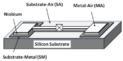
A total of 5 qubit styles were designed and simulated using Ansys HFSS and Q3D software, and shown in Figs. 4 through 8. We refer to these different designs as MOD A through MOD E. Participation factors were determined by calculating the corresponding energy based on the electric fields present at particular surfaces and interfaces within the build. Hypothetical layers possessing a dielectric constant of [12] were placed between the substrate and overlying metallization (SM), the top surface of the substrate exposed to air (SA) and the metallization surfaces exposed to air (MA). Continuous layers of uniform thickness were assumed but because the thickness of these layers was not known a priori, the units of the calculated surface participation factors in Table I are . For a given layer, multiplying the participation factor by the thickness and tan() gives the reciprocal of the qubit quality factor Q assuming no other sources of loss.
Because the thicknesses of these contamination layers are presumed to be much thinner ( 10 nm) than the dimensions of the constitutive elements of the qubit metallization, the constraints on the domain discretization necessary to produce a credible numerical solution made conventional simulation impractial. Instead we adopted a strategy of calculating the effective electric field strength at key interfaces by first assuming no contamination layer and extrapolating the solution to a different dielectric constant than those on either side of the original interface. The effective fields were calculated by matching the appropriate components of the electric fields as prescribed by the boundary conditions between two dielectric layers:
| (1) | |||
| (2) |
where is the component of the field parallel to the interface, is that normal to the interface, superscript 1 refers to the hypothetical contamination layer and 2 the actual dielectric material present in the simulation (e.g: silicon for the substrate surfaces or vacuum for the free surfaces). Combining Equations 1 and 2, we arrive at the effective electric field in the contamination layer with dielectric constant :
| (3) |
Calculations of the surface participation factors, , were then conducted by projecting a uniform electric field strength throughout the layer thickness, , and integrating over the corresponding surface, :
| (4) |
where is the conjugate of and is the total energy of the system.
| MOD A | MOD B | MOD C | MOD D | MOD E | |
|---|---|---|---|---|---|
| SM | 3.68x | 1.10x | 3.46x | 2.15x | 1.20x |
| SA | 1.24x | 3.32x | 9.10x | 5.04x | 2.38x |
| MA | 7.20x | 1.62x | 3.80x | 1.80x | 6.0x |
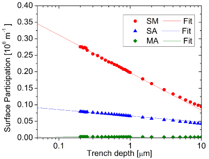
Additional complications are that the electric field diverges near corners, and that the etching procedures used in the fabrication of the 2D transmon qubits result in some degree of recess of the substrate surface in the qubit pocket. It is thus important to incorporate the effects of trenching in the surface participation calculations. HFSS models were generated that included both 200 nm thick Nb metallization and a variation in the pocket trench depth. Identical qubit junctions, treated as lumped elements, were used for all of the MOD’s under investigation. Because the singular nature of the electric fields near the edges of the Nb metallization can lead to convergence issues in the simulations of trench depths less than 200-300 nm, we restricted the modeling to trenches greater than this thickness and extrapolated participation factors of the various interfaces according to a lograrithmic fit with respect to the trench depth. Because the electric field strength obeys a dependence for a thin metallic sheet [14] where is the distance from the sheet edge, the integrand in Equation 4 should scale as for small , leading to the logarithmic dependence in surface participation as confirmed in Figure 2. Table I contains the extrapolated participation factors to a trench depth of 50 nm for all of the designs, demonstrating that the substrate-metal (SM) interface participation varies by a factor of x over the different designs, the substrate-air (SA) interface participation varies about a factor of x, and while the metal-air (MA) interface participation varies over two orders of magnitude, its participation is substantially less than that of the SM and SA interfaces and is likely not contributing to loss.
Substrate participation was simulated using HFSS in a similar manner as that used for the surface participation factors. The substrate participation asymptotes to a constant value in the limit that the trench depth approaches zero. In this limit, in which the magnitude of the electric fields present in the dielectric substrate and in vacuum are equal, the substrate participation approaches for all of the MOD’s. Here and in all simulations we have assumed the dielectric constant of the substrate as .
Chip sizes were and , small enough that the fundamental chip mode was located above GHz. Each chip consists of a single Ohm feedline, off of which four CPW resonators (also Ohm) are each terminated by a transmon qubit of identical design. The resonator frequencies are staggered at with a coupling quality factor of . Given qubit-resonator coupling strengths in the range of , we calculate the Purcell loss [15] to be negligible in all our experiments with qubit frequencies targeted in the range. The qubit chip is back mounted to a PC board and placed in a light tight enclosure to minimize exposure to IR radiation [4, 5]. Most measurements were done using the high power readout [6]. To ensure no residual effects from the readout are present [3] we varied the repetition time or employed standard low power QND measurements for many samples (but not all) and observed no noticeable differences. The input attenuation and filtering to the sample varied slightly between experiments to test thermal dephasing [16], but these variations were found to have little impact, if any, on times. However, because times are typically near there is still room for improvement for future experiments. The output lines included PAMTECH GHz isolators (model CWJ0312KI) and a 4K HEMT amplifier by CalTech.
III Fabrication,testing and results
The qubits were fabricated on high resistivity (cm) silicon using a standard niobium (Nb) recipe with a hydrogen fluoride (HF) clean just prior to the deposition of the sputtered Nb. The junctions are fabricated using a cold develop and acetone lift off at room temperature. Each wafer received a Huang clean to remove organic and inorganic contaminants from the wafer surface. Within 30 minutes prior to the 200 nm Nb deposition each wafer received a 2 min. 100:1 HF clean to remove the surface SiOx. After the HF treatment each wafer received a 5 min water rinse. After the water rinse and dry there is a thin SiOx layer on the surface. Next, a chlorine based RIE etch was performed which slightly over etches the silicon, etching approximately nm into the silicon. The aluminum - aluminum oxide - aluminum Josepshon junction is fabricated using a Dolan bridge [17] employing PMMA/MMA processing steps. The aluminum makes contact to the niobium after applying a gentle low power ion mill clean prior to the aluminum deposition. We have tested additional qubits (data not shown) with slight modifications to the pre-cleans prior to the niobium deposition but found no deviations from the data reported here, and similarly a junction lift-off in Microposit Remover 1165 at C was also found not to affect coherence times.
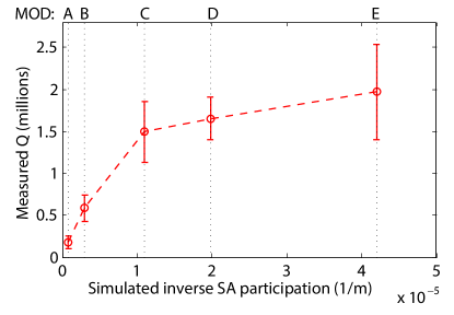
The measured times are translated into quality factors in order to remove effects from frequency variations of the qubits; within the range of qubit frequencies measured, no frequency dependence of the quality factor was found. The results are summarized in Fig. 3, where the measured quality factors are plotted against the inverse of simulated SA surface loss participation values. If coherence times were limited by SA loss we would expect Q to linearly scale with the inverse of the participation values. Each data point represents the mean quality factor of eight qubits, and the error bar is the standard deviation divided by the square root of the number of measured qubits. Each is obtained by averaging typically on the order of a few hours to account for known fluctuations. We observe a dramatic improvement in Q between MOD A and MOD B qubits, consistent with predictions based on surface loss. When plotted against SM or MA inverse surface participation values (not shown) the results look very similar, which leads us to the conclusion that at present the data is not sufficient to ascertain which of the interfaces dominates. High MOD qubits appear to saturate near indicating a loss contribution of unknown origin, which could potentially include substrate loss, loss due to quasi-particles [3], residual coupling to resistive metallic components housing the qubits or other mechanisms. Nonetheless, it is possible to place an upper bound on the bulk loss of the silicon of though we believe the actual number is likely less.
IV Conclusion
In conclusion, we present a systematic study of quality factors in qubits with widely varying degrees of surface participation. Results indicate that depending on the design, qubits can be either limited by surface loss (low-MOD qubits) or an additional loss mechanism (high-MOD qubits) that is currently not well understood. The experimental results are not sufficient for us to make any claims on which surface dominates surface loss. We believe the methods applied here should allow for optimal design of qubits for long coherence to enable relevant multi-qubit implementations. The results also motivate the development of cleaning methods to potentially enable smaller footprint qubits with good coherence in the future, as well as the development of additional strategies to understand new loss mechanisms for high MOD qubits. We would like to acknowledge useful discussions and contributions from Mary Beth Rothwell, George Keefe and Cyril Cabral.
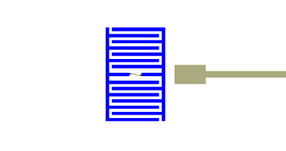
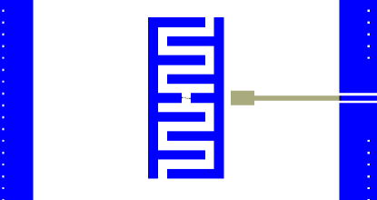
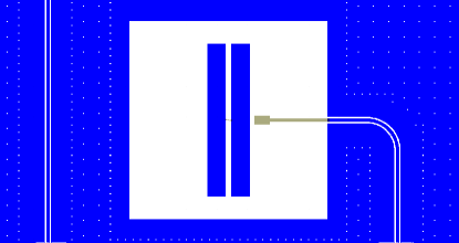
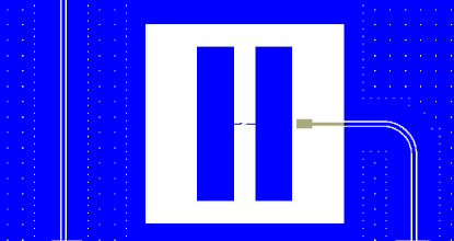
V Pictures of the qubit designs
Below are figures showing each of the five MOD designs in detail. Note that all qubits are placed inside a grounding box of dimension . This box is only fully visible for MODs D and E. MODs A and B were also tested with a larger coupling capacitor to increase the signal-to-noise ratio. The data indicates no appreciable effect on , which is not surprising given that the calculated Purcell limit is much larger than the observed coherence times.
References
- [1] J. M. Martinis, K. B. Cooper, R. McDermott, M. Steffen, M. Ansmann, K. D. Osborn, K. Cicak, S. Oh, D. P. Pappas, R. W. Simmonds, and C. C. Yu, “Decoherence in josephson qubits from dielectric loss,” Phys. Rev. Lett., vol. 95, no. 21, p. 210503, Nov 2005.
- [2] L. Sun, L. DiCarlo, G. Catelani, L. S. Bishop, D. I. Schuster, B. R. Johnson, G. A. Yang, L. Frunzio, L. Glazman, M. H. Devoret, and R. Schoelkopf, “Measurements of quasiparticle tunneling dynamics in a band-gap-engineered transmon qubit,” Physical Review Letters, vol. 108, p. 230509, 2012.
- [3] C. Wang, Y. Y. Gao, I. M. Pop, U. Vool, C. Axline, T. Brecht, R. W. Heeres, L. Frunzio, M. H. Devoret, G. Catelani, L. I. Glazman, and R. J. Schoelkopf, “Measurement and control of quasiparticle dynamics in a superconducting qubit,” Nature Communications, vol. 5, p. 5836, 2014.
- [4] R. Barends, J. Wenner, M. Lenander, Y. Chen, R. C. Bialczak, J. Kelly, E. Lucero, P. O’Malley, M. Mariantoni, D. Sank, H. Wang, T. C. White, Y. Yin, J. Zhao, A. N. Cleland, J. M. Martinis, and J. J. A. Baselmans, “Minimizing quasiparticle generation from stray infrared light in superconducting quantum circuits,” Appl. Phys. Lett., vol. 99, p. 113507, 2011.
- [5] A. D. Corcoles, J. M. Chow, J. M. Gambetta, C. Rigetti, J. R. Rozen, G. A. Keefe, M. B. Rothwell, M. B. Ketchen, and M. Steffen, “Protecting superconducting qubits from radiation,” Appl. Phys. Lett., vol. 99, p. 4, 2011.
- [6] M. D. Reed, L. DiCarlo, B. R. Johnson, L. Sun, D. I. Schuster, L. Frunzio, and R. J. Schoelkopf, “High fidelity readout in circuit quantum electrodynamics using the jaynes-cummings nonlinearity,” Phys. Rev. Lett., vol. 105, p. 173601, 2010.
- [7] M. Sandberg, M. R. Vissers, T. A. Ohki, J. Gao, J. Aumentado, M. Weides, and D. P. Pappas, “Radiation-suppressed superconducting quantum bit in a planar geometry,” Appl. Phys. Lett., vol. 102, p. 072601, 2013.
- [8] J. Wenner, R., R. Bialczak, Y. Chen, J. Kelly, E. Lucero, M. Mariantoni, A. Megrant, P. O’Malley, D. Sank, A. Vainsencher, H. Wang, T. White, Y. Yin, J. Zhao, A. Cleland, and J. M. Martinis, “Surface loss simulations of superconducting coplanar waveguide resonators,” Appl. Phys. Lett., vol. 99, p. 113513, 2011.
- [9] K. Geerlings, S. Shankar, E. Edwards, L. Frunzio, R. Schoelkopf, and M. H. Devoret, “Improving the quality factor of microwave compact resonators by optimizing their geometrical parameters,” Appl. Phys. Lett., vol. 100, p. 192601, 2012.
- [10] A. Megrant, C. Neill, R. Barends, B. Chiaro, Y. Chen, L. Feigl, J. Kelly, E. Lucero, M. Mariantoni, P. O’Malley, D. Sank, A. Vainsencher, J. Wenner, T. White, Y. Yin, J. Zhao, C. Palmstrøm, J. M. Martinis, and A. N. Cleland, “Planar superconducting resonators with internal quality factors above one million,” Appl. Phys. Lett., vol. 100, p. 113510, 2012.
- [11] C. M. Quintana, A. Megrant, Z. Chen, A. Dunsworth, B. Chiaro, R. Barends, B. Campbell, Y. Chen, I.-C. Hoi, E. Jeffrey, J. Kelly, J. Y. Mutus, P. J. J. O’Malley, C. Neill, P. Roushan, D. Sank, A. Vainsencher, J. Wenner, T. C. White, A. N. Cleland, and J. M. Martinis, “Characterization and reduction of microfabrication-induced decoherence in superconducting quantum circuits,” Appl. Phys. Lett., vol. 105, p. 062601, 2014.
- [12] O. Dial, D. T. McClure, S. Poletto, G. A. Keefe, M. B. Rothwell, J. M. Gambetta, D. W. Abraham, J. M. Chow, and M. Steffen, “Bulk and surface loss in superconducting transmon qubits,” Superconductor Science and Technology, vol. 29, no. 4, p. 044001, 2016.
- [13] J. Koch, T. M. Yu, J. Gambetta, A. A. Houck, D. I. Schuster, J. Majer, A. Blais, M. H. Devoret, S. M. Girvin, and R. J. Schoelkopf, “Charge-insensitive qubit design derived from the cooper pair box,” Phys. Rev. A, vol. 76, no. 4, p. 042319, Oct 2007.
- [14] J. Jackson, Classical Electrodynamics, 2nd Ed., pp. 77–78, 1975.
- [15] A. Houck, J. Schreier, B. Johnson, J. Chow, J. Koch, J. Gambetta, D. Schuster, L. Frunzio, M. Devoret, S. Girvin, and R. Schoelkopf, “Controlling the spontaneous emission of a superconducting transmon qubit,” Phys. Rev. Lett., vol. 101, p. 080502, 2008.
- [16] C. Rigetti, J. M. Gambetta, S. Poletto, B. Plourde, J. M. Chow, A. D. Corcoles, J. A. Smolin, S. T. Merkel, J. Rozen, G. A. Keefe, M. B. Rothwell, M. B. Ketchen, , and M. Steffen, “Superconducting qubit in a waveguide cavity with a coherence time approaching 0.1 ms,” Phys. Rev. B, vol. 86, p. 100506(R), 2012.
- [17] G. J. Dolan, “Offset masks for lift-off processing,” Appl. Phys. Lett., vol. 31, pp. 337 – 339, 1977.