Spectroscopy and Dynamics of a Two-Dimensional Electron Gas on top of Ultrathin Helium Films on Cu(111)
Abstract
Electrons in image-potential states on the surface of bulk helium represent a unique model system of a two-dimensional electron gas. Here, we investigate their properties in the extreme case of reduced film thickness: a monolayer of helium physisorbed on a single-crystalline (111)-oriented Cu surface. For this purpose we have utilized a customized setup for time-resolved two-photon photoemission (2PPE) at very low temperatures under ultra-high vacuum conditions. We demonstrate that the highly polarizable metal substrate increases the binding energy of the first () image-potential state by more than two orders of magnitude as compared to the surface of liquid helium. An electron in this state is still strongly decoupled from the metal surface due to the large negative electron affinity of helium and we find that even one monolayer of helium increases its lifetime by one order of magnitude compared to the bare Cu(111) surface.
pacs:
73.20.-r, 78.47.J-, 79.60.-i, 79.60.DpTwo-dimensional (2D) electron systems attract interest since more than years. Apart from sheet structures such as graphene, 2D electron systems exist at heterostructures like semiconductor-semiconductor Stormer79ssc ; Davies98 , semiconductor-insulator Ando82rmp ; Davies98 ; Monarkha04 , oxide-oxide Stemmer14annurev , or metal-insulator interfaces Gudde05pss , and on the surface of condensed materials with negative electron affinity Cole73rmp ; Andrei97 ; Monarkha04 . Two limiting cases are known: dense electron layers with Fermi temperatures in the hundred K range in quantum wells, particularly of semiconductor heterostructures Stormer79ssc ; Davies98 ; and very dilute 2D electron gases in the image-potential states on top of condensed Helium Cole73rmp ; Andrei97 ; Monarkha04 with Fermi temperatures in the mK range, and spacing of the excited states in the microwave regime Grimes76prb . For electrons on the bulk surface of He, the maximum density is small: for more than electrons per cm-2 the layer becomes unstable Edelman80pu and the electron gas remains in the classical regime. Early, it was realized that the density of such electron layers can be significantly increased by growing He films of finite thickness on top of a substrate with large permittivity Ikezi81prb ; Peeters83prl . For a Å He film on a doped silicon substrate, for example, densities of up to cm-2 have been reported Etz84prl . Such densities offer the possibility to study the quantum regime of this almost ideal 2D electron system including effects as Wigner crystallization and quantum-melting Peeters83prl as long as the electron gas is well decoupled from the substrate. For very thin films, however, the coupling to the substrate will be strongly influenced by surface roughness and impurities of the substrate which can lead to lateral localization and enhanced tunneling through the film Etz84prl ; Gunzler96ss . The study of this regime thus requires the combination of advanced surface science and cryogenic techniques.
In this Letter, we investigate the limiting case of a monolayer (ML) of He on an atomically flat single-crystalline metal substrate and present a study of the electron transfer dynamics of the image-potential states on this archetypical 2D system. Image potential states on clean and rare gas covered metal surfaces already proved to be ideal model systems for the electron transfer dynamics at surfaces and through thin dielectric layers, by theory and by experiment, in particular by two-photon photoemission (2PPE) studies Echeni04ssr . For thin films of the heavier rare gases, it has been shown that the coupling of the image-potential states to the metal strongly depends on the electron affinity of the film which represents a tunnel barrier in the case of negative electron affinity Berthold02cpl ; Marinica02prl ; Berthold04apa ; Gudde05pss . He films are expected to exhibit a particular high barrier (the electron affinity of condensed He is eV Sommer64prl ), which offers the possibility to create a 2D electron gas with high binding energy and very long lifetime even for very small thicknesses. He films are also unique with regard to their structure. Whereas all other rare gases, including Neon, form islands at sub-monolayer coverage and solid single-crystals at larger thicknesses Schlic92ss ; Wolf96prb ; Berthold04apa ; Berthold04ss , sub-monolayer of He grow as uniform 2D gas layer and thick He films are liquid because of the large zero-point energy and the weak van der Waals interaction Note1 . Despite of these outstanding quantum properties, the 2D electron gas on ultrathin He films was not investigated until now, mainly because of experimental challenges.
2PPE of He films requires very low temperatures Nieder02prl ; Nieder05prb , shielding from thermal radiation of the environment which leads to desorption of the layers Nieder02prl ; Nieder05prb , and highly sensitive electron spectroscopy at low laser intensities. Tackling these challenges with customized equipment, we present results on binding energies and lifetimes of the image potential states on ultrathin He films physisorbed on a single-crystalline Cu(111) substrate.
Figure 1 shows the experimental setup. The liquid He (LHe) bath cryostat of our UHV chamber (base pressure of mbar) was operated at a He pressure of typically mbar corresponding to a LHe temperature below 1 K Clement55pr . Well-defined Cu(111) surfaces have been prepared by in-situ epitaxially growth of approximate hundred ML thick Cu films on a Ru(0001) single crystal. The latter was thermally coupled to the cryostat by a thin, spot-welded single-crystalline tungsten rod. With this setup, sample temperatures below 1.2 K were obtained Kossler11dr ; Kossler14prb . He films were prepared by dosing purified He gas through a capillary aiming at the sample. We compensated the unavoidable loss of He due to laser stimulated desorption by a controlled continuous flow of He, which allows for the variation of the adlayer density within the laser spot. Further details of the sample preparation and characterization are described in the Supplemental Material supplemental .
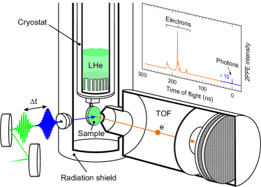
In order to avoid electronically stimulated desorption of the He layers by the K black body radiation of the environment Nieder02prl ; Nieder05prb , the whole cryostat and the time-of-flight (TOF) spectrometer used for electron spectroscopy ( meV energy resolution) were surrounded by radiation shields cooled to K by liquid nitrogen (LN2) Kossler11dr ; Kossler14prb . During the experiment, these shields were completely closed except of a tiny 2 mm2 aperture for the laser beams [Fig. 1].
The laser setup provided p-polarized femtosecond laser pulses in the visible (vis) and ultraviolet (uv) spectral range with variable time delay at a repetition rate of kHz Damm09prb . Typical photon energies and pulse lengths of eV, fs and eV, fs enabled excitation of the first two image-potential states with the uv pulses but simultaneously avoided an excessive background signal due to one-photon photoemission. The average laser power of each laser beam was reduced to only W ( nJ/pulse) as a compromise between He desorption and 2PPE intensity.
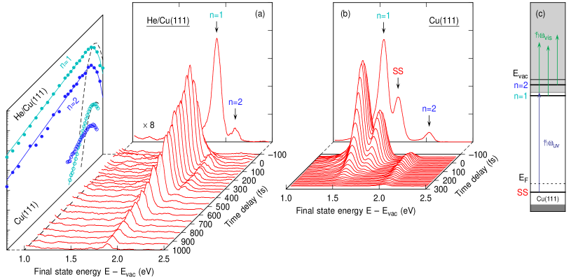
Figure 2 shows two time-resolved series of 2PPE spectra at normal emission obtained from the He covered (a) and bare (b) Cu(111) surface. Both series show three prominent features. The peaks denoted as and are assigned to the first two members of the Rydberg-like series of initially unoccupied image-potential states which are populated by the uv pump pulses and subsequently photoemitted by the vis probe pulses, as illustrated in (c)Note2 . The signals of the ()- and ()-states appear for the bare surface at final state energies of and eV, respectively (rear panel of (b)). This corresponds to binding energies with respect to of eV and eV. We note that theses binding energies are slightly smaller than values reported for Cu(111) bulk samples Wolf96prb ; Weinelt02jp ; Damm09prb ; Borisov06prb . The peak at eV denoted by SS results from direct photoemission from the partially occupied intrinsic Shockley-type surface state by non-resonant 2PPE with one uv and one vis photon and is only visible for temporal overlapping pump and probe pulses. At the -point this state has a binding energy of eV with respect to the Fermi level.
The 2PPE spectra of the He covered Cu(111) surface of Fig. 2(a) have been recorded at a He background pressure of mbar which supports a coverage of one monolayer under laser irradiation, as it will be shown below. Compared to the pristine Cu(111) surface the signal of the SS is almost completely quenched and the ()- and ()-maxima show a considerable blue shift to final states energies of 1.94 and 2.13 eV with respect to , respectively. At these energies, also the ()-state is degenerated with the projected Cu bulk bands [Fig. 3] and is in fact an image-potential resonance.
The energy shift is almost completely caused by a reduction of the binding energies by about a factor of two ( eV, eV), whereas the weakly polarizable He film reduces the work function only marginally by 50 meV [Fig. 3]. Thus, even one monolayer of He strongly decouples the image-potential states from the metal surface. Despite this decoupling, the binding energies are much larger than those reported for electrons on the surface of LHe ( meV Cole69prl ), because of the strong electron attraction by the highly polarizable metal substrate underneath the He film.
Lifetimes of electrons excited into the image-potential states at the -point have been determined by measuring the 2PPE intensity at the respective energies as function of the time delay between the uv and the vis laser pulses [Fig. 2, left panel]. The lifetimes have been extracted from best fits (solid lines) using a rate-equation model assuming single-exponential population decay. On the bare Cu(111) surface, the states and show lifetimes of fs and fs, respectively supplemental .
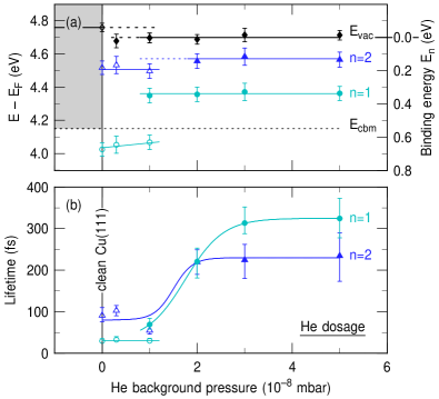
Adsorption of a monolayer of He drastically changes the electron dynamics in the image-potential states: increases by one order of magnitude to fs [Fig. 3(b)] despite the fact that the state becomes an image-potential resonance. The lifetime of the -state, which is already an image-potential resonance on the bare Cu(111) surface, is less affected. It increases only by a factor of two to fs.
For coverage dependent data, the He density within the illuminated spot has been calibrated by systematic 2PPE measurements as a function of while keeping the laser intensities constant. The results are summarized in Fig. 3 where (a) and (b) are plotted as a function of . For increasing , slightly drops by only 50 meV. The peaks assigned to the () states on the pristine Cu surface decrease continuously and vanish for mbar. Simultaneously, two new peaks with lower binding energies appear in the 2PPE spectrum, which we assign to the first two image-potential states on the He covered areas. Just at mbar, we still observe the ()-peak assigned to the uncovered areas and already the ()-peak assigned to the covered areas supplemental . This might be surprising at first glance, since submonolayers of physisorbed He do not grow as 2D islands like the heavier rare-gases, but form instead a 2D gas. In our experiment, the coexistence of covered and uncovered areas results from the competition of adsorption and laser induced desorption which causes a variation of the coverage across the spot profile of the laser. The desorption rate is, however, small. We estimate it to be ML per laser shot supplemental . The assignment of the states is consistent with their lifetimes as a function of . The lifetimes of the states assigned to bare Cu(111) areas remain almost constant while those of the states assigned to the He covered areas increase with and saturate above mbar, which we interpret as the formation of a saturated monolayer. We do not expect the formation of the more weakly bound second monolayer supplemental .
On the Cu(111) surface, the change of the decay dynamics upon He adsorption is an interplay of decoupling of the wave functions from the metal and energy shift with respect to the Cu bulk bands. Whereas the decoupling increases the lifetime, the shift into resonance with the Cu bulk bands reduces it, because it opens the additional decay channel of elastic resonant charge transfer into the bulk Borisov06prb ; Hofer16ss .
The decoupling is caused by the strong Pauli repulsion by the closed-shell He atoms. This repulsion constitutes a high tunneling barrier for the whole series of image-potential states and extend up to 1.3 eV above the vacuum level for a thick layer of liquid He Sommer64prl . The image force attraction induced by the metal substrate reduces this barrier, whereas the larger density of the monolayer due to the much stronger He-metal compared to He-He dispersion forces increases it Broomall76prb . The actual barrier height can be estimated from the above-threshold maximum of the kinetic energy distributions of secondary electrons, which in good approximation corresponds to the top of the barrier with respect to the vacuum level. Our data and those of Ref. Kossler11dr yield 0.8 eV for this quantity; in combination with the ()-binding energies this results in effective barrier heights of 1.15 and 0.96 eV for the () and ()-states, respectively.
These barriers push the image-potential states further away from the metal and strongly reduce the wave function overlap with the Cu bulk and surface states. This overlap is the crucial quantity for the lifetime of image-potential states and resonances, because it determines the efficiency of both inelastic and elastic decay Echeni04ssr ; Borisov06prb . The latter dominates the decay of image-potential resonances and is responsible for their general much shorter lifetimes as compared to image-potential states at the same barrier height Damm09prb . Against this background, the observed increase of the ()-lifetime on Cu(111) by one order of magnitude is unprecedentedly large and clearly opens up new possibilities for detailed investigations of 2D electron gases.
In the framework of the present study, the choice of Cu(111) films on Ru(0001) as a substrate was dictated by technical constrains. In a further optimized experimental setup one would make use of substrates like Cu(100) or Ag(100), on which the image-potential states are located far from the projected bulk bands Chulkov99ss2 . The present data allow us to predict the degree of decoupling by a He layer on these substrates by comparing the measured ()-resonance lifetime of He/Cu(111) with that of a hypothetical resonance on bare Cu(111) at the same energy. The dominant elastic contribution of its lifetime can be calculated reliably within a multiple scattering approach that provides the electron reflectivity at the surface barrier as a function of energy Hofer16ss . Potential parameters of Cu(111) Chulkov99ss2 yield for this quantity 0.74 (0.65) at an energy of 0.1 eV (0.2 eV) above the band edge, which corresponds to an elastic lifetime of only 4 fs (2.9 fs). Even if we allow an uncertainty of the exact band edge position in our Cu(111) films of 0.1 eV, this estimation demonstrates that the decoupling of a single ML of He is capable to enhance the ()-lifetime by up to two orders of magnitude. This is about 30 times larger as compared to Ar Berthold02cpl .
In conclusion, we have shown that the ultimate model system of a 2D electron gas on a thin He film grown on an atomically smooth single crystalline metal surface is accessible with time-resolved photoemission spectroscopy. We find that its lifetime is under such conditions only limited by tunneling and not by surface defects. In a further optimized setup, which reaches temperatures below 1 K as required for the growth of thicker He layers, our results let us expect to realize lifetimes of several hundred picoseconds even on an only 2-ML-thick He film on Cu(100) or Ag(100). The binding energy on such thin film is still large enough to support high electron densities without becoming instable due to ripplon formation Etz84prl . In combination with angle-resolved photoemission spectroscopy, this opens the possibility to observe phenomena such as Wigner crystallization and melting into a degenerate 2D electron gas within momentum space.
We gratefully acknowledge funding by the Deutsche Forschungsgemeinschaft through Project No. GU495/2 and SFB 1083. SK and PF acknowledge support by the Deutsche Forschungsgemeinschaft through project No. FE246/2 and by the Munich-Centre for Advanced Photonics through project No. MAP B.1.4.
References
- (1) H. L. Störmer, R. Dingle, A. C. Gossard, W. Wiegmann, and M. D. Sturge, Sol. Stat. Comm. 29, 705 (1979).
- (2) J. Davies, The Physics of Low-dimensional Semiconductors: An Introduction (Cambridge University Press, Cambridge, 1998).
- (3) T. Ando, A. B. Fowler, and F. Stern, Rev. Mod. Phys. 54, 437 (1982).
- (4) Y. P. Monarkha and K. Kono, Two-Dimensional Coulomb Liquids and Solids (Springer-Verlag, Berlin, Heidelberg, 2004).
- (5) S. Stemmer and S. J. Allen, Annu. Rev. Mater. Res. 44, 151 (2014).
- (6) J. Güdde and U. Höfer, Prog. Surf. Sci. 80, 49 (2005).
- (7) M. W. Cole, Rev. Mod. Phys. 46, 451 (1974).
- (8) Two-Dimensional Electron Systems, edited by E. Y. Andrei (Kluwer Academic Publishers, Dordrecht, The Netherlands, 1997).
- (9) C. C. Grimes, T. R. Brown, M. L. Burns, and C. L. Zipfel, Phys. Rev. B 13, 140 (1976).
- (10) V. S. Edel’man, Sov. Phys. Usp. 23, 227 (1980).
- (11) H. Ikezi and P. M. Platzman, Phys. Rev. B 23, 1145 (1981).
- (12) F. M. Peeters and P. M. Platzman, Phys. Rev. Lett. 50, 2021 (1983).
- (13) H. Etz, W. Gombert, W. Idstein, and P. Leiderer, Phys. Rev. Lett. 53, 2567 (1984).
- (14) T. Günzler, B. Bitnar, G. Mistura, S. Neser, and P. Leiderer, Surface Science 361-362, 831 (1996).
- (15) P. M. Echenique, R. Berndt, E. V. Chulkov, T. Fauster, A. Goldmann, and U. Höfer, Surf. Sci. Rep. 52, 219 (2004).
- (16) W. Berthold, P. Feulner, and U. Höfer, Chem. Phys. Lett. 358, 502 (2002).
- (17) D. C. Marinica, C. Ramseyer, A. G. Borisov, D. Teillet-Billy, J. P. Gauyacq, W. Berthold, P. Feulner, and U. Höfer, Phys. Rev. Lett. 89, 046802 (2002).
- (18) W. Berthold, F. Rebentrost, P. Feulner, and U. Höfer, Appl. Phys. A 78, 131 (2004).
- (19) W. T. Sommer, Phys. Rev. Lett. 12, 271 (1964).
- (20) H. Schlichting and D. Menzel, Surf. Sci. 272, 27 (1992).
- (21) M. Wolf, E. Knoesel, and T. Hertel, Phys. Rev. B 54, R5295 (1996).
- (22) W. Berthold, P. Feulner, and U. Höfer, Surf. Sci. 548, L13 (2004).
- (23) A phase transition, which might be interpreted as solidification, has been observed for He/Pt(111) at coverages beyond 70% of saturation by means of thermal desorption spectroscopy Nieder02prl ; Nieder05prb . This transition, however, could not be verified by electron spectroscopy as yet Kossler11dr ; Kossler14prb .
- (24) T. Niedermayer, H. Schlichting, D. Menzel, S. H. Payne, and H. J. Kreuzer, Phys. Rev. Lett. 89, 126101 (2002).
- (25) T. Niedermayer, H. Schlichting, D. Menzel, S. H. Payne, and H. J. Kreuzer, Phys. Rev. B 71, 045427 (2005).
- (26) J. R. Clement, J. K. Logan, and J. Gaffney, Phys. Rev. 100, 743 (1955).
- (27) S. Kossler, Dissertation, Technische Universität München, 2011.
- (28) S. Kossler, P. Feulner, and J.-P. Gauyacq, Phys. Rev. B 89, 165410 (2014).
- (29) See Supplemental Material at [http://…] for more details, which includes Refs. Kossler11dr ; Kossler14prb ; Wolf96prb ; Weinelt02jp ; Damm09prb ; Berthold04apa ; Borisov06prb ; Schubert12prb ; Hofer16ss ; Nieder05prb ; Tang92ssl ; Zaremba77prb ; Perreau82ss .
- (30) M. Weinelt, J. Phys.-Condens. Mat. 14, R1099 (2002).
- (31) A. Damm, K. Schubert, J. Güdde, and U. Höfer, Phys. Rev. B 80, 205425 (2009).
- (32) A. G. Borisov, E. V. Chulkov, and P. M. Echenique, Phys. Rev. B 73, 073402 (2006).
- (33) K. Schubert, A. Damm, S. V. Eremeev, M. Marks, M. Shibuta, W. Berthold, J. Güdde, A. G. Borisov, S. S. Tsirkin, E. V. Chulkov, and U. Höfer, Phys. Rev. B 85, 205431 (2012).
- (34) U. Höfer and P. M. Echenique, Surf. Sci. 643, 203 (2016).
- (35) K. Tang and J. P. Toennies, Surface Science 279, L203 (1992).
- (36) E. Zaremba and W. Kohn, Phys. Rev. B 15, 1769 (1977).
- (37) J. Perreau and J. Lapujoulade, Surface Science 122, 341 (1982).
- (38) The ()-state is in fact an image-potential resonance on Cu(111), because it is degenerated with Cu bulk bands Wolf96prb ; Weinelt02jp ; Damm09prb ; Borisov06prb .
- (39) E. M. Cole and H. M. Cohen, Phys. Rev. Lett. 23, 1238 (1969).
- (40) J. R. Broomall, W. D. Johnson, and D. G. Onn, Phys. Rev. B 14, 2819 (1976).
- (41) E. V. Chulkov, V. M. Silkin, and P. M. Echenique, Surf. Sci. 437, 330 (1999).