A CMOS silicon spin qubit
Silicon, the main constituent of microprocessor chips, is emerging as a promising materialMaune et al. (2012); Pla et al. (2012); Kawakami et al. (2014); Veldhorst et al. (2014); Muhonen et al. (2014); Veldhorst et al. (2015) for the realization of future quantum processorsKane (1998); Loss and Divincenzo (1998). Leveraging its well-established complementary metal-oxide-semiconductor (CMOS) technology would be a clear asset to the development of scalable quantum computing architecturesHill et al. (2015); Pica et al. (2016) and to their co-integration with classical control hardwareLevy et al. (2011). Here we report a silicon quantum bit (qubit) device made with an industry-standard fabrication processBarraud et al. (2012). The device consists of a two-gate, p-type transistor with an undoped channel. At low temperature, the first gate defines a quantum dot (QD) encoding a hole spin qubit, the second one a QD used for the qubit readout. All electrical, two-axis control of the spin qubit is achieved by applying a phase-tunable microwave modulation to the first gate. Our result opens a viable path to qubit up-scaling through a readily exploitable CMOS platform.
Localized spins in semiconductors can be used to encode elementary bits of quantum information Kane (1998); Loss and Divincenzo (1998). Spin qubits were demonstrated in a variety of semiconductors, starting from GaAs-based heterostructures Petta et al. (2005); Koppens et al. (2006); Hanson et al. (2007). In this material, and all III-V compounds in general, electron spins couple to the nuclear spins of the host crystal via the hyperfine interaction resulting, in a relatively short inhomogeneous dephasing time, (a few tens of ns in GaAs Koppens et al. (2008)). This problem can be cured to a large extent by means of echo-type spin manipulation sequences and notch filtering techniques Bluhm et al. (2010); Lange et al. (2010); Malinowski et al. (2016). In natural silicon, however, the hyperfine interaction is weaker, being due to the content of 29Si, the only stable isotope with a non-zero nuclear spin. Measured values range between ns and s Pla et al. (2012); Maune et al. (2012); Wu et al. (2014); Kawakami et al. (2014). Experiments carried out on electron spin qubits in isotopically purified silicon ( of spinless 28Si), have even allowed extending to s Veldhorst et al. (2014). Following these improvements in spin coherence time, silicon-based spin qubits classify among the best solid-state qubits, at the single qubit level. Recently, the first two-qubit logic gate with control-NOT functionality was also demonstrated Veldhorst et al. (2015), marking the next essential milestone towards scalable processors.
Surface-code quantum computing architectures, possibly the only viable option to date, require large numbers (eventually millions) of qubits individually controlled with tunable nearest-neighbor couplings Bravyi and Kitaev ; Dennis et al. (2002). Their implementation is a considerable challenge since it implies dealing with issues such as device-to-device variability, multi-layer electrical wiring, and, most likely, on-chip classical electronics (amplifiers, multiplexers, etc) for qubit control and readout. This is where the well-established CMOS technology becomes a compelling tool. A possible strategy is to export qubit device implementations developed within academic-scale laboratories into large-scale CMOS platforms. This approach is likely to require significant process integration development at the CMOS foundry. Here we present an alternative route, where an existing process flow for the fabrication of CMOS transistors is taken as a starting point, and it is adapted to obtain devices with qubit functionality.
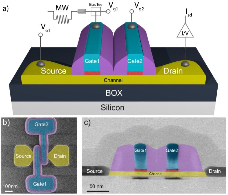
We use a microelectronics technology based on mm Silicon-On-Insulator (SOI) wafers. Our qubit device, schematically shown in Fig. 1a, is derived from silicon nanowire field-effect transistors Barraud et al. (2012). It consists of a -nm-thick and -nm-wide undoped silicon channel with p-doped source and drain contact regions, and two nm wide parallel top gates, side covered by insulating silicon nitride spacers. A scanning-electron-microscopy top view, and a transmission-electron-microscopy cross-sectional view are shown in Fig. 1b and 1c, respectively. At low temperature, hole QDs are created by charge accumulation below the gates Voisin et al. (2016). The double gate layout enables the formation of two QDs in series, QD1 and QD2, with occupancies controlled by voltages and applied to gates 1 and 2, respectively (see supplementary section 2). We tune charge accumulation to relatively small numbers, N, of confined holes ( per dot). In this regime, the QDs exhibit a discrete energy spectrum with level spacing in the 0.1 - 1 meV range, and Coulomb charging energy meV.
In a simple scenario where spin-degenerate QD levels get progressively filled by pairs of holes, each QD carries a spin for N=odd and a spin for N=even. By setting N=odd in both dots two spin-1/2 qubits can be potentially encoded, one for each QD. This is equivalent to the (1,1) charge configuration, where the first and second digits denote the charge occupancies of QD1 and QD2, respectively. In practice, here we shall demonstrate full two-axis control of the first spin only, and use the second spin for initialization and readout purposes. Tuning the double QD to a parity-equivalent (1,1) (0,2) charge transition, initialization and readout of the qubit relies on the so-called Pauli spin blockade mechanism Ono et al. (2002); Hanson et al. (2007). In this particular charge transition, tunneling between dots can be blocked by spin selection rule. Basically, for a fixed, say “up”, spin orientation in QD2, tunneling will be allowed if the spin in QD1 is “down” and it will forbidden by the Pauli exclusion principle if the spin in QD1 is “up” i.e. a triplet (1,1) state is not coupled to the singlet (0,2) state. This charge/spin configuration can be identified through characteristic experimental signatures Danon and Nazarov (2009); Nadj-Perge et al. (2010); Li et al. (2015) associated with the Pauli blockade effect discussed above (see supplementary section 3).
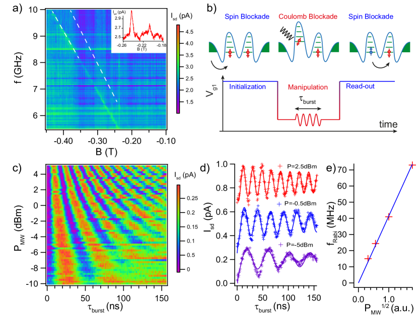
We now turn to the procedure for spin manipulation. In a recent work on similar devices with only one gate, we found that hole g-factors are anisotropic and gate dependent Voisin et al. (2016), denoting strong spin-orbit coupling (see also Ref. Li et al. (2015)). This implies the possibility to perform electric-dipole spin resonance (EDSR), namely to drive coherent hole-spin rotations by means of microwave-frequency (MW) modulation of a gate voltage (see supplementary section 4). Here we apply the MW modulation to Gate 1 in order to rotate the spin in QD1. Spin rotations result in the lifting of spin blockade. In a measurement of source-drain current as a function of magnetic field, , (perpendicular to the chip) and MW frequency, , EDSR is revealed by narrow ridges of increased currentNadj-Perge et al. (2010). The data set in Fig. 2a shows two of such current ridges, one clearly visible and the other one rather faint. Both ridges follow a linear dependence consistent with the spin resonance condition , where is Planck’s constant, the Bohr magneton, and the hole Landé g-factor along the magnetic-field direction. From the slopes of the two ridges we extract two g-factor values, and comparable to those reported before Voisin et al. (2016). Based on the relative intensities of the current ridges we ascribe these g-factor values to QD1 and QD2, respectively. We have observed similar EDSR features at other working points (i.e. different parity-equivalent (1,1) (0,2) transitions) and in two distinct devices (see supplementary section 4).
To perform controlled spin rotations, and hence demonstrate qubit functionality, we replace continuous-wave gate modulation with MW bursts of tunable duration, . During spin manipulation, we prevent charge leakage due to tunneling from QD1 to QD2 by simultaneously detuning the double QD to a Coulomb-blockade regime Koppens et al. (2006) (see Fig. 2b). Following each burst, is abruptly increased to bring the double dot back to the parity-equivalent (1,1) (0,2) resonant transition. At this stage, a hole can tunnel from QD1 to QD2 with a probability proportional to the unblocked spin component in QD1 (i.e. the probability amplitude for spin-up if QD2 hosts a spin-down state). The resulting (0,2)-like charge state “decays” by emitting a hole into the drain, and a hole from the source is successively fed back to QD1, thereby restoring the initial (1,1)-like charge configuration. The net effect is the transfer of one hole from source to drain, which will eventually contribute to a measurable average current. (In principle, in case not all (1,1)-like states are Pauli blocked, the described charge cycle may occur more than once during the readout-initialization portion of the same period, until the parity-equivalent (1,1) (0,2) becomes spin blocked again and the system is re-initialized for the next manipulation cycle.)
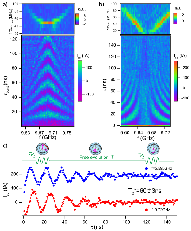
We chose a modulation period of ns, of which ns are devoted to spin manipulation and ns to readout and initialization. Figure 2c) shows as a function of MW power and at a spin-resonance condition for mT. The observed current modulation is a hallmark of coherent Rabi oscillations of the spin in QD1, also explicitly shown by selected cuts at three different MW powers (Fig. 2d)). As expected, the Rabi frequency, , increases linearly with the MW voltage amplitude, which is proportional to (Fig. 2e)). At the highest power, we reach a remarkably large MHz, comparable to the highest reported values for electrically controlled semiconductor spin qubits van den Berg et al. (2013). Figure 3a) shows a color plot of revealing the characteristic chevron pattern associated to Rabi oscillations Kawakami et al. (2014). The fast Fourier transform (FFT) of , calculated for each value, is shown in the upper panel. It exhibits a peak at the Rabi frequency with the expected hyperbolic dependence on frequency detuning , where GHz is the resonance frequency at the corresponding mT.
To evaluate the inhomogeneous dephasing time during free-evolution, we perform a Ramsey fringes-like experiment, which consists in applying two short, phase coherent, MW pulses separated by a delay time . The proportionality between the qubit rotation angle, , and is used to calibrate both pulses to a rotation (see sketch in Fig. 3c). For each value, exhibits oscillations at frequency decaying on a timescale ns (see Fig. 3b)). Extracted current oscillations at fixed frequency are presented in Fig. 3c). At resonance (), the two pulses induce rotations around the same axis (say the x-axis of the rotating frame). The effect of a finite is to change the rotation axis of the second pulse relative to the first one. Alternatively, two-axis control can be achieved also at resonance () by varying the relative phase of the MW modulation between the two pulses. For a Ramsey sequence --, the first pulse induces a rotation around and the second one around , , and for , , and , respectively. The signal then oscillates with as shown in the insets to Fig. 4a, and the oscillation amplitude vanishes with on a time scale (see Fig. 4a).
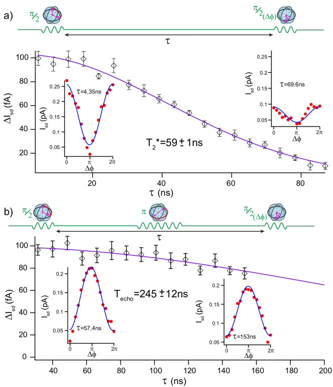
The intrinsic coherence time associated with the dynamics of the dominant dephasing source can be accessed by means of a Hahn-echo experiment, where a pulse is introduced half way between the two pulses, as sketched in Fig. 4b. The amplitude of the oscillations in (insets to Fig. 4b)) decays on a coherence time ns. The relatively short and can hardly be explained by the dephasing from nuclear spins. In fact, even if little is known about the hyperfine interaction strength for confined holes in silicon, we would expect it to be even smaller than the one for electrons. Testelin et al. (2009). Alternative decoherence mechanisms could dominate, such as paramagnetic impurities, charge noise, or the stronger hyperfine interaction with boron dopants diffused from the contact regions. Further studies will be necessary to establish statistically relevant values for the coherence time scales and to identify their origin.
In essence, we have shown that a p-type silicon field-effect transistor fabricated within an industry-standard CMOS process line can exhibit hole spin qubit functionality with fast, all-electrical, two-axis control. In the prospect of realizing large-scale quantum computing architectures, this result opens a favorable scenario with some clear follow-up milestones. The next step is to advance from the simple, yet limited transistor-like structures studied here to more elaborate qubit designs, incorporating additional important elements such as single-shot qubit read-out, and enabling scalable qubit-to-qubit coupling schemes. In addition, a systematic investigation of qubit performances, including the benchmarking of hole qubits against their electron counterparts, has to be performed in the short term. The use of state-of-the-art CMOS technology, with its well-established fabrication processes and integration capabilities, is going to be a clear asset in all these tasks. At a later stage, it should also favor the co-integration of classical cryogenic control hardware.
References
- Maune et al. (2012) B. M. Maune, M. G. Borselli, B. Huang, T. D. Ladd, P. W. Deelman, K. S. Holabird, A. A. Kiselev, I. Alvarado-Rodriguez, R. S. Ross, A. E. Schmitz, M. Sokolich, C. A. Watson, M. F. Gyure, and A. T. Hunter, Nature 481, 344 (2012).
- Pla et al. (2012) J. J. Pla, K. Y. Tan, J. P. Dehollain, W. H. Lim, J. J. L. Morton, D. N. Jamieson, A. S. Dzurak, and A. Morello, Nature 489, 541 (2012).
- Kawakami et al. (2014) E. Kawakami, P. Scarlino, D. R. Ward, F. R. Braakman, D. E. Savage, M. G. Lagally, M. Friesen, S. N. Coppersmith, M. A. Eriksson, and L. M. K. Vandersypen, Nature nanotechnology 9, 666 (2014).
- Veldhorst et al. (2014) M. Veldhorst, J. C. C. Hwang, C. H. Yang, A. W. Leenstra, B. de Ronde, J. P. Dehollain, J. T. Muhonen, F. E. Hudson, K. M. Itoh, A. Morello, and A. S. Dzurak, Nature nanotechnology 9, 981 (2014).
- Muhonen et al. (2014) J. T. Muhonen, J. P. Dehollain, A. Laucht, F. E. Hudson, R. Kalra, T. Sekiguchi, K. M. Itoh, D. N. Jamieson, J. C. McCallum, A. S. Dzurak, and A. Morello, Nature nanotechnology 9, 986 (2014).
- Veldhorst et al. (2015) M. Veldhorst, C. H. Yang, J. C. C. Hwang, W. Huang, J. P. Dehollain, J. T. Muhonen, S. Simmons, a. Laucht, F. E. Hudson, K. M. Itoh, a. Morello, and a. S. Dzurak, Nature , 0 (2015).
- Kane (1998) B. E. Kane, Nature 393, 133 (1998).
- Loss and Divincenzo (1998) D. Loss and D. P. Divincenzo, Phys. Rev. A 57, 120 (1998).
- Hill et al. (2015) C. D. Hill, E. Peretz, S. J. Hile, M. G. House, M. Fuechsle, S. Rogge, M. Y. Simmons, and L. C. L. Hollenberg, Science Advances e1500707, 1 (2015).
- Pica et al. (2016) G. Pica, B. W. Lovett, R. N. Bhatt, T. Schenkel, and S. a. Lyon, Physical Review B 93, 035306 (2016).
- Levy et al. (2011) J. E. Levy, M. S. Carroll, A. Ganti, C. A. Phillips, A. J. Landahl, T. M. Gurrieri, R. D. Carr, H. L. Stalford, and E. Nielsen, New Journal of Physics 13, 083021 (2011).
- Barraud et al. (2012) S. Barraud, R. Coquand, M. Cassé, M. Koyama, J. Hartmann, C. Comboroure, C. Vizioz, F. Aussenac, O. Faynot, and T. Poiroux, IEEE Electron Device Letter 33, 1526 (2012).
- Petta et al. (2005) J. R. Petta, A. C. Johnson, J. M. Taylor, E. A. Laird, A. Yacoby, M. D. Lukin, C. M. Marcus, M. P. Hanson, and A. C. Gossard, Science (New York, N.Y.) 309, 2180 (2005).
- Koppens et al. (2006) F. H. L. Koppens, C. Buizert, K. J. Tielrooij, I. T. Vink, K. C. Nowack, T. Meunier, L. P. Kouwenhoven, and L. M. K. Vandersypen, Nature 442, 766 (2006).
- Hanson et al. (2007) R. Hanson, L. Kouwenhoven, and J. Petta, Reviews of Modern Physics 79 (2007).
- Koppens et al. (2008) F. H. L. Koppens, K. C. Nowack, and L. M. K. Vandersypen, Physical Review Letters 100, 236802 (2008).
- Bluhm et al. (2010) H. Bluhm, S. Foletti, I. Neder, M. Rudner, D. Mahalu, V. Umansky, and A. Yacoby, Nature Physics 7, 109 (2010).
- Lange et al. (2010) G. D. Lange, Z. H. Wang, V. V. Dobrovitski, and R. Hanson, Science 330, 60 (2010).
- Malinowski et al. (2016) F. K. Malinowski, F. Martins, P. D. Nissen, E. Barnes, M. S. Rudner, S. Fallahi, G. C. Gardner, M. J. Manfra, C. M. Marcus, and F. Kuemmeth, arXiv:1601.0667 (2016).
- Wu et al. (2014) X. Wu, D. R. Ward, J. R. Prance, D. Kim, J. K. Gamble, R. T. Mohr, Z. Shi, D. E. Savage, M. G. Lagally, M. Friesen, S. N. Coppersmith, and M. a. Eriksson, Proceedings of the National Academy of Sciences of the United States of America 111, 11938 (2014).
- (21) S. B. Bravyi and A. Y. Kitaev, arXiv:quant-ph/9811052v1 .
- Dennis et al. (2002) E. Dennis, A. Kitaev, A. Landahl, and J. Preskill, Journal of Mathematical Physics 43, 4452 (2002).
- Voisin et al. (2016) B. Voisin, R. Maurand, S. Barraud, M. Vinet, X. Jehl, M. Sanquer, J. Renard, and S. De Franceschi, Nano letters 16, 88 (2016).
- Ono et al. (2002) K. Ono, D. Austing, Y. Tokura, and S. Tarucha, Science 297, 1313 (2002).
- Danon and Nazarov (2009) J. Danon and Y. V. Nazarov, Physical Review B 80, 041301 (2009).
- Nadj-Perge et al. (2010) S. Nadj-Perge, S. M. Frolov, J. W. W. van Tilburg, J. Danon, Y. V. Nazarov, R. Algra, E. P. A. M. Bakkers, and L. P. Kouwenhoven, Physical Review B 81, 201305 (2010).
- Li et al. (2015) R. Li, F. E. Hudson, A. S. Dzurak, and A. R. Hamilton, Nano letters 15, 7314 (2015).
- Koppens et al. (2007) F. H. L. Koppens, D. Klauser, W. a. Coish, K. C. Nowack, L. P. Kouwenhoven, D. Loss, and L. M. K. Vandersypen, Physical review letters 99, 106803 (2007).
- van den Berg et al. (2013) J. W. G. van den Berg, S. Nadj-Perge, V. S. Pribiag, S. R. Plissard, E. P. A. M. Bakkers, S. M. Frolov, and L. P. Kouwenhoven, Physical Review Letters 110, 066806 (2013).
- Testelin et al. (2009) C. Testelin, F. Bernardot, B. Eble, and M. Chamarro, Physical Review B 79, 195440 (2009).
Methods
A detailed description of the device fabrication process is given in Supplementary section1. All measurements were performed in a dilution refrigerator with a base temperature of mK. The direct source-drain current providing qubit readout was measured by means of a current/voltage amplifier with a gain of . All low-frequency lines are low-pass filtered at base temperature with two stage RC filters. High frequency signals applied to Gate 1 come for a 20 GHz bandwidth coaxial line with distributed 36 dBm attenuation along the dilution fridge for thermalization. A home-made bias tee on the sample board allows combination of microwave and low-frequency signals on the gate. One channel of an arbitrary wave generator (Tektronix AWG5014C) is used to generate the two-level modulation driving the device between Coulomb blockade (qubit manipulation phase) and Pauli blockade (qubit readout and initialization). Two other channels of the AWG define square pulses to control the I and Q inputs of the MW source. MW bursts and the two-level gate modulation are combined by means of a diplexer before reaching the dilution fridge.