Simple DRAM and Virtual Memory Abstractions
to Enable Highly Efficient Memory Subsystems
Vivek Seshadri
CMU-CS-16-106
April 2016
School of Computer Science
Computer Science Department
Carnegie Mellon University
Pittsburgh, PA 15213
Thesis Committee
Todd C. Mowry (Co-chair)
Onur Mutlu (Co-chair)
David Andersen
Phillip B. Gibbons
Rajeev Balasubramonian, University of Utah
Submitted in partial fulfillment of the requirements
for the degree of Doctor of Philosophy.
Copyright © 2016 Vivek Seshadri
This research was sponsored by the National Science Foundation under grant numbers CNS-0720790, EEC-0951919, CCF-1116898, CCF-1212962, CNS-1320531, CNS-1423172, CCF-0953246, CCF-1147397, and CNS-1409723, the Defense Advanced Research Projects Agency under grant number FA8721-5-C-0003, Princeton University under grant number 00001751, Semiconductor Research Corporation under grant number 2012HJ2320, Intel ISTC-CC, Intel URO Memory Hierarchy Program, Gigascale Systems Research Center, AMD, Google, IBM, Intel, Nvidia, Oracle, Samsung, and VMware. The views and conclusions contained in this document are those of the author and should not be interpreted as representing the official policies, either expressed or implied, of any sponsoring institution, the U.S. government or any other entity.
Keywords: Efficiency, Memory Subsystem, Virtual Memory, DRAM, Data Movement, Processing in Memory, Fine-grained Memory Management
Abstract
In most modern systems, the memory subsystem is managed and accessed at multiple different granularities at various resources. The software stack typically accesses data at a word granularity (typically 4 or 8 bytes). The on-chip caches store data at a cache line granularity (typically 64 bytes). The commodity off-chip memory interface is optimized to fetch data from main memory at a cache line granularity. The main memory capacity itself is managed at a page granularity using virtual memory (typically 4KB pages with support for larger super pages). The off-chip commodity DRAM architecture internally operates at a row granularity (typically 8KB). In this thesis, we observe that this curse of multiple granularities results in significant inefficiency in the memory subsystem.
We identify three specific problems. First, page-granularity virtual memory unnecessarily triggers large memory operations. For instance, with the widely-used copy-on-write technique, even a single byte update to a virtual page results in a full 4KB copy operation. Second, with existing off-chip memory interfaces, to perform any operation, the processor must first read the source data into the on-chip caches and write the result back to main memory. For bulk data operations, this model results in a large amount of data transfer back and forth on the main memory channel. Existing systems are particularly inefficient for bulk operations that do not require any computation (e.g., data copy or initialization). Third, for operations that do not exhibit good spatial locality, e.g., non-unit strided access patterns, existing cache-line-optimized memory subsystems unnecessarily fetch values that are not required by the application over the memory channel and store them in the on-chip cache. All these problems result in high latency, and high (and often unnecessary) memory bandwidth and energy consumption.
To address these problems, we present a series of techniques in this thesis. First, to address the inefficiency of existing page-granularity virtual memory systems, we propose a new framework called page overlays. At a high level, our framework augments the existing virtual memory framework with the ability to track a new version of a subset of cache lines within each virtual page. We show that this simple extension is very powerful by demonstrating its benefits on a number of different applications.
Second, we show that the analog operation of DRAM can perform more complex operations than just store data. When combined with the row granularity operation of commodity DRAM, we can perform these complex operations efficiently in bulk. Specifically, we propose RowClone, a mechanism to perform bulk data copy and initialization operations completely inside DRAM, and Buddy RAM, a mechanism to perform bulk bitwise logical operations using DRAM. Both these techniques achieve an order-of-magnitude improvement in performance and energy-efficiency of the respective operations.
Third, to improve the performance of non-unit strided access patterns, we propose Gather-Scatter DRAM (GS-DRAM), a technique that exploits the module organization of commodity DRAM to effectively gather or scatter values with any power-of-2 strided access pattern. For these access patterns, GS-DRAM achieves near-ideal bandwidth and cache utilization, without increasing the latency of fetching data from memory.
Finally, to improve the performance of the protocol to maintain the coherence of dirty cache blocks, we propose the Dirty-Block Index (DBI), a new way of tracking dirty blocks in the on-chip caches. In addition to improving the efficiency of bulk data coherence, DBI has several applications, including high-performance memory scheduling, efficient cache lookup bypassing, and enabling heterogeneous ECC for on-chip caches.
Acknowledgments
The last chapter of this dissertation acknowledges the collaborations with my fellow graduate students. These collaborations have been critical in keeping my morale high throughout the course of my Ph.D.
Many people have directly or indirectly played a significant role in the success of my Ph.D. Words alone may not be sufficient to express my gratitude to these people. Yet, I would like to thank
| Todd & Onur, | for trusting me and giving me freedom, despite some tough initial years, for constantly encouraging me to work hard, and for keeping me focused |
| Mike & Phil, | for being more than just collaborators |
| Dave & Rajeev, | for making the ending as less painful as possible |
| Deb, | for ensuring that I did not have to worry about anything but research |
| Donghyuk & Yoongu, | for teaching me everything I know about DRAM |
| Lavanya, | for being more than just a lab mate |
| Michelle, Tunji, & Evangelos, | for sharing the secrets of the trade |
| Gena, Chris, & Justin, | for giving me a different perspective in research and life |
| other members of SAFARI, | for all the valuable and enjoyable discussions |
| people @ PDL & CALCM, | for all the feedback and comments |
| Frank, Rick, Vyas, & other members of AB league, | for making squash an integral part of my life |
| Stan & Patty, | for their warming smile every time I visit UC |
| Gopu, | for being my best roommate for the better part of my Ph.D. |
| Shane, | for being a part of an important decade in my life |
| G, RawT, KL, Coolie, & BAP, | for making my life @ Pittsburgh enjoyable |
| Vyas, | for teaching me (mostly necessary) life skills |
| PJ, | for giving me hope |
| Veda, Tomy, Murali, Hetu, & Captain, | for all the gyan |
| Ashwati, Usha, & Shapadi, | for all the chai, and random life discussions |
| James & DSha, | for all the discussions, rants, and squash |
| Ranjan, SKB, Sudha, & Joy, | for the complete TeleTaaz experience |
| Sharads, Sumon, Kaushik, & KJ et al., | for food and company |
| IGSA folks, | for the much-needed distraction |
| Jyo, Pave, Sail, Vimal, Karthi, and Jayavel, | for always being the friends in need |
| MahimaSri, NiMeg, Wassim, Yogi, & Pro Club, | for making Redmond my second home in the US |
| PK & Kaavy, | for my go-to whatsapp group |
| DHari, | for putting up with me |
| Vikram, | for making my path in life smooth |
| Appa & Amma, | for freedom and support. |
Chapter 1 Introduction
In recent years, energy-efficiency has become a major design factor in systems. This trend is fueled by the ever-growing use of battery-powered hand-held devices on the one end, and large-scale data centers on the other end. To ensure high energy-efficiency, all the resources in a system (e.g., processor, caches, memory) must be used efficiently.
To simplify system design, each resource typically exposes an interface/abstraction to other resources in the system. Such abstractions allow system designers to adopt newer technologies to implement a resource without modifying other resources. However, a poor abstraction to a resource that does not expose all its capabilities can significantly limit the overall efficiency of the system.
1.1 Focus of This Dissertation: The Memory Subsystem
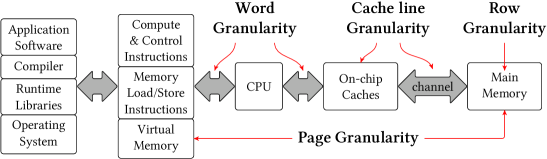
This dissertation focuses on the efficiency of the memory subsystem. Main memory management in a modern system has two components: 1) memory mapping (affects capacity management, protection, etc.), and 2) memory access (reads, writes, etc.). We observe that in existing systems, there is a mismatch in the granularity at which memory is mapped and accessed at different resources, resulting in significant inefficiency. Figure 1.1 shows the different layers of the system stack and their interaction with different memory resources.
1.1.1 Different Granularities of Data Storage and Access
First, most modern operating systems (OS) ubiquitously use virtual memory [60] to manage main memory capacity. To map virtual memory to physical memory, virtual memory systems use a set of mapping tables called page tables. In order to keep the overhead of the page tables low, most virtual memory systems typically manage memory at a large granularity (4KB pages or larger super pages). Second, to access memory, the instruction set architecture (ISA) exposes a set of load and store instructions to the software stack. To allow efficient representation of various data types, such instructions typically allow software to access memory at a small granularity (e.g., 4B or 8B words). Third, any memory request generated by load/store instructions go through a hierarchy of on-chip caches all the way to the off-chip main memory. In order to lower the cost of the cache tag stores and the memory interface, the on-chip caches and the off-chip memory interface are typically optimized to store and communicate data at a granularity wider than a single word (e.g., 64B cache lines). Finally, to reduce cost-per-bit, commodity DRAM architectures internally operate at a row granularity (typically 8KB). It is clear that data are stored and accessed at different granularities in different memory resources. We identify three problems that result from this mismatch in granularity.
1.1.2 The Curse of Multiple Granularities
First, we observe that the page-granularity virtual memory management can result in unnecessary work. For instance, when using the copy-on-write technique, even a write to a single byte can trigger a full page copy operation. Second, existing off-chip memory interfaces only expose a read-write abstraction to main memory. As a result, to perform any operation, the processor must read all the source data from main memory and write back the results to main memory. For operations that involve a large amount of data, i.e., bulk data operations, this approach results in a large number of data transfers on the memory channel. Third, many access patterns trigger accesses with poor spatial locality (e.g., non-unit strided accesses). With existing caches and off-chip interfaces optimized for cache line granularity, such access patterns fetch a large amount of data not required by the application over the memory channel and store them in the on-chip cache.
All these problems result in high latency, high (and often unnecessary) memory bandwidth, and inefficient cache utilization. As a result, they affect the performance of not only the application performing the operations, but also the performance of other co-running applications. Moreover, as data movement on the memory channel consumes high energy [57], these operations also lower the overall energy-efficiency of the system. Chapter 2 motivates these problems in more detail using case studies.
1.2 Related Work
Several prior works have proposed mechanisms to improve memory efficiency. In this section, we discuss some closely related prior approaches. We group prior works based on their high level approach and describe their shortcomings.
1.2.1 New Virtual Memory Frameworks
Page-granularity virtual memory hinders efficient implementation of many techniques that require tracking memory at a fine granularity (e.g., fine-grained memory deduplication, fine-grained metadata management). Prior works have proposed new frameworks to implement such techniques (e.g., HiCAMP [48], Mondrian Memory Protection [236], architectural support for shadow memory [159, 249, 161, 250, 253]). Unfortunately, these mechanisms either significantly change the existing virtual memory structure, thereby resulting in high cost, or introduce significant changes solely for a specific functionality, thereby reducing overall value.
1.2.2 Adding Processing Logic Near Memory (DRAM)
One of the primary sources of memory inefficiency in existing systems is the data movement. Data has to travel off-chip buses and multiple levels of caches before reaching the CPU. To avoid this data movement, many works (e.g., Logic-in-Memory Computer [209], NON-VON Database Machine [14], EXECUBE [127], Terasys [78], Intelligent RAM [169], Active Pages [166], FlexRAM [117, 70], Computational RAM [66], DIVA [61] ) have proposed mechanisms and models to add processing logic close to memory. The idea is to integrate memory and CPU on the same chip by designing the CPU using the memory process technology. While the reduced data movement allows these approaches to enable low-latency, high-bandwidth, and low-energy data communication, they suffer from two key shortcomings.
First, this approach of integrating processor on the same chip as memory greatly increases the overall cost of the system. Second, DRAM vendors use a high-density process to minimize cost-per-bit. Unfortunately, high-density DRAM process is not suitable for building high-speed logic [169]. As a result, this approach is not suitable for building a general purpose processor near memory, at least with modern logic and high-density DRAM technologies.
1.2.3 3D-Stacked DRAM Architectures
Some recent architectures [145, 107, 6] use 3D-stacking technology to stack multiple DRAM chips on top of the processor chip or a separate logic layer. These architectures offer much higher bandwidth to the logic layer compared to traditional off-chip interfaces. This enables an opportunity to offload some computation to the logic layer, thereby improving performance. In fact, many recent works have proposed mechanisms to improve and exploit such architectures (e.g., [21, 20, 244, 69, 82, 255, 218, 95, 75, 153, 90, 74, 68, 28, 24, 135]). Unfortunately, despite enabling higher bandwidth compared to off-chip memory, such 3D-stacked architectures are still require data to be transferred outside the DRAM chip, and hence can be bandwidth-limited. In addition, thermal constraints constrain the number of chips that can be stacked, thereby limiting the memory capacity. As a result, multiple 3D-stacked DRAMs are required to scale to large workloads.
1.2.4 Adding Logic to the Memory Controller
Many prior works have proposed mechanisms to export certain memory operations to the memory controller with the goal of improving the efficiency of the operation (e.g., Copy Engine [248] to perform bulk copy or initialization, Impulse [39] to perform gather/scatter operations, Enhanced Memory Controller [88] to accelerate dependent cache misses). Recent memory technologies which stack DRAM chips on top of a logic layer containing the memory controller [107, 6] will likely make this approach attractive. Although these mechanisms definitely reduce the pressure on the CPU and on-chip caches, they still have to go through the cache-line-granularity main memory interface, which is inefficient to perform these operations.
1.2.5 Supporting Fine-grained Memory Accesses in DRAM
A number of works exploit the module-level organization of DRAM to enable efficient fine-grained memory accesses (e.g., Mini-rank [252], Multi-Core DIMM [19], Threaded memory modules [231], Scatter/Gather DIMMs [38]). These works add logic to the DRAM module that enables the memory controller to access data from individual chips rather than the entire module. Unfortunately, such interfaces 1) are much costlier compared to existing memory interfaces, 2) potentially lower the DRAM bandwidth utilization, and 3) do not alleviate the inefficiency for bulk data operations.
1.2.6 Improving DRAM Latency and Parallelism
A number of prior works have proposed new DRAM microarchitectures to lower the latency of DRAM access or enable more parallelism within DRAM. Approaches employed by these works include 1) introducing heterogeneity in access latency inside DRAM for a low cost (e.g., Tiered-Latency DRAM [137], Asymmetric Banks [204], Dynamic Asymmetric Subarrays [146], Low-cost Interlinked Subarrays [46]), 2) improving parallelism within DRAM (e.g., Subarray-level Parallelism [125], parallelizing refreshes [47], Dual-Port DRAM [138]), 3) exploiting charge characteristics of cells to reduce DRAM latency (e.g., Multi-clone-row DRAM [49], Charge Cache [89]), 4) reducing the granularity of internal DRAM operation through microarchitectural changes (e.g., Half-DRAM [246], Sub-row activation [224]), 5) adding SRAM cache to DRAM chips [93], 6) exploiting variation in DRAM (e.g., Adaptive Latency DRAM [136], FLY-DRAM [45]), and 7) better refresh scheduling and refresh reduction (e.g., [144, 77, 211, 29, 104, 163, 122, 175, 119]. While many of these approaches will improve the performance of various memory operations, they are still far from mitigating the unnecessary bandwidth consumed by certain memory operations (e.g., bulk data copy, non-unit strided access).
1.2.7 Reducing Memory Bandwidth Requirements
Many prior works have proposed techniques to reduce memory bandwidth consumption of applications. Approaches used by these works include 1) data compression (e.g., [173, 172, 171, 170, 65, 222]), 2) value prediction (e.g., [188, 141]), 3) load approximation (e.g., [221, 152]), 4) adaptive granularity memory systems (e.g., [242, 243]), and 5) better caching to reduce the number of memory requests (e.g., [194, 106, 176]). Some of these techniques require significant changes to the hardware (e.g., compression, adaptive granularity memory systems). Having said that, all these approaches are orthogonal to the techniques proposed in this dissertation.
1.2.8 Mitigating Contention for Memory Bandwidth
One of the problems that result from bulk data operations is the contention for memory bandwidth, which can negatively affect the performance of applications co-running in the system. A plethora of prior works have proposed mechanisms to mitigate this performance degradation using better memory request scheduling (e.g., [156, 154, 157, 124, 123, 213, 214, 76, 133, 134, 225, 26, 103, 114, 27, 247]). While these works improve overall system performance and fairness, they do not fundamentally reduce the bandwidth consumption of the applications performing the bulk operations.
1.3 Thesis Statement and Overview
Our goal in this thesis is to improve the overall efficiency of the memory subsystem without significantly modifying existing abstractions and without degrading the performance/efficiency of applications that do not use our proposed techniques. Towards this end, our thesis is that,
we can exploit the diversity in the granularity at which different hardware resources manage memory to mitigate the inefficiency that arises from that very diversity. To this end, we propose to augment existing processor and main memory architectures with some simple, low-cost features that bridge the gap resulting from the granularity mismatch.
Our proposed techniques are based on two observations. First, modern processors are capable of tracking data at a cache-line granularity. Therefore, even though memory capacity is managed at a larger page granularity, using some simple features, it should be possible to enable more efficient implementations of fine-grained memory operations. Second, although off-chip memory interfaces are optimized to access cache lines, we observe that the commodity memory architecture has the ability to internally operate at both a bulk row granularity and at a fine word granularity.
We exploit these observations to propose a new virtual memory framework that enables efficient fine-grained memory management, and a series of techniques to exploit the commodity DRAM architecture to efficiently perform bulk data operations and accelerate memory operations with low spatial locality.
1.4 Contributions
This dissertation makes the following contributions.
-
1.
We propose a new virtual memory framework called page overlays that allows memory to be managed at a sub-page (cache line) granularity. The page overlays framework significantly improves the efficiency of several memory management techniques, e.g., copy-on-write, and super pages. Chapter 3 describes our framework, its implementation, and applications in detail.
-
2.
We observe that DRAM internally operates at a large, row granularity. Through simple changes to the DRAM architecture, we propose RowClone, a mechanism that enables fast and efficient bulk copy operations completely within DRAM. We exploit RowClone to accelerate copy-on-write and bulk zeroing, two important primitives in modern systems. Chapter 5 describes RowClone and its applications in detail.
-
3.
We observe that the analog operation of DRAM has the potential to efficiently perform bitwise logical operations. We propose Buddy RAM, a mechanism that exploits this potential to enable efficient bulk bitwise operations completely with DRAM. We demonstrate the performance benefits of this mechanism using 1) a database bitmap index library, and 2) an efficient implementation of a set data structure. Chapter 6 describes Buddy RAM in detail.
-
4.
We observe that commodity DRAM architectures heavily interleave data of a single cache line across many DRAM devices and multiple arrays within each device. We propose Gather-Scatter DRAM (GS-DRAM), which exploits this fact to enable the memory controller to gather or scatter data of common access patterns with near ideal efficiency. We propose mechanisms that use GS-DRAM to accelerate non-unit strided access patterns in many important applications, e.g., databases. Chapter 7 describes GS-DRAM and its applications in detail.
-
5.
Our mechanisms to perform operations completely in DRAM require appropriate dirty cache lines from the on-chip cache to be flushed. We propose the Dirty-Block Index (DBI) that significantly improves the efficiency of this flushing operation. Chapter 8 describes DBI and several other of its potential applications in detail.
Chapter 2 The Curse of Multiple Granularities
As mentioned in Chapter 1, different memory resources are managed and accessed at a different granularity — main memory capacity is managed at a page (typically 4KB) granularity, on-chip caches and off-chip memory interfaces store and access data at a cache line (typically 64B) granularity, DRAM internally performs operations at a row granularity (typically 8KB), and the applications (and CPU) access data at a small word (typically 4B or 8B) granularity. This mismatch results in a significant inefficiency in the execution of two important classes of operations: 1) bulk data operations, and 2) operations with low spatial locality. In this chapter, we discuss the sources of this inefficiency for each of these operations using one example operation in each class.
2.1 Bulk Data Operations
A bulk data operation is one that involves a large amount of data. In existing systems, to perform any operation, the corresponding data must first be brought to the CPU L1 cache. Unfortunately, this model results in high inefficiency for a bulk data operation, especially if the operation does not involve any computation on the part of the processor (e.g., data movement). To understand the sources of inefficiency in existing systems, let us consider the widely-used copy-on-write [79] technique.
2.1.1 The Copy-on-Write Technique
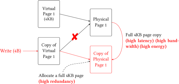
Figure 2.1 shows how the copy-on-write technique works. When the system wants to copy the data from the virtual page V1 to the virtual page V2, it simply maps the page V2 to the same physical page (P1) to which V1 is mapped to. Based on the semantics of virtual memory, any read access to either virtual page is directed to the same page, ensuring correct execution. In fact, if neither of the two virtual pages are modified after the remap, the system would have avoided an unnecessary copy operation. However, if one of the virtual pages, say V2, does receive a write, the system must perform three steps. First, the operating system must identify a new physical page (P2) from the free page list. Second, it must copy the data from the original physical page (P1) to the newly identified page (P2). Third, it must remap the virtual page that received the write (V2) to the new physical page (P2). After these steps are completed, the system can execute the write operation.
2.1.2 Sources of Inefficiency in Executing Copy-on-Write
Existing interfaces to manage and access the memory subsystem result in several sources of inefficiency in completing a copy-on-write operation. First, existing virtual memory systems manage main memory at a large page granularity. Therefore, even if only a single byte or word is modified in the virtual page V2, the system must allocate and copy a full physical page. This results in high memory redundancy. Second, the CPU accesses data at a word or at best a vector register granularity. Existing systems must therefore perform these copy operations one word or a vector register at a time. This results in high latency and inefficient use of the CPU. Third, all the cache lines involved in the copy operation must be transferred from main memory to the processor caches. These cache line transfers result in high memory bandwidth consumption and can potentially cause cache pollution. Finally, all the data movement between the CPU, caches, and main memory consumes significant amounts of energy.
Ideally, instead of copying an entire page of data, the system should eliminate all the redundancy by remapping only the data that is actually modified. In a case where the entire page needs to be copied, the system should all the unnecessary data movement by performing the copy operation completely in main memory.
2.2 Fine-grained Operations with Low Spatial Locality
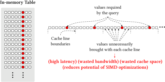
As we mentioned in Chapter 1, the on-chip caches and the off-chip memory interface are both optimized to store and communicate wide cache lines (e.g., 64B). However, the data types typically used by applications are much smaller than a cache line. While access patterns with good spatial locality benefit from the cache-line-granularity management, existing systems incur high inefficiency when performing operations with low spatial locality. Specifically, non-unit strided access patterns are common in several applications, e.g., databases, scientific computing, and graphics. To illustrate the shortcomings of existing memory interfaces, we use an example of an in-memory database table.
2.2.1 Accessing a Column from a Row-Oriented Database Table
In-memory databases are becoming popular among many applications. A table in such a database consist of many records (or rows). Each record in turn consists of many fields (or columns). Typically, a table is stored either in the row-oriented format or the column-oriented format. In the row-oriented format or row store, all fields of a record are stored together. On the other hand, in the column-oriented format or column store, the values of each field from all records are stored together. Depending on the nature of the query being performed on the table, one format may be better suited than the other. For example, the row store is better suited for inserting new records or executing transactions on existing records. On the other hand, the column store is better suited for executing analytical queries that aim to extract aggregate information from one or few fields of many records.
Unfortunately, neither organization is better suited for both transactions and analytical queries. With the recently growing need for real-time analytics, workloads that run both transactions and analytics on the same system, referred to as Hybrid Transaction/Analytics Processing or HTAP [17], are becoming important. Accessing a column of data from a row store results in a strided access pattern.
2.2.2 Shortcomings of Strided Access Patterns
Figure 2.2 shows the shortcomings of accessing a column of data from a database table that is stored as a row store. For ease of explanation, we assume that each record fits exactly into a cache line. As shown in the figure, each cache line contains only one useful value. However, since the caches and memory interface in existing systems are heavily optimized to store and access cache lines, existing systems have to fetch more data than necessary to complete the strided access operation. In the example shown in the figure, the system has to bring eight times more data than necessary to access a single column from a row store. This amplification in the amount of data fetched results in several problems. First, it significantly increases the latency to complete the operation, thereby degrading the performance of the application. Second, it results in inefficient use of memory bandwidth and on-chip cache space. Finally, since different values of the strided access pattern are stored in different cache lines, it is difficult to enable SIMD (single instruction multiple data) optimizations for the computation performing the strided access pattern.
Ideally, the memory system should be able to identify the strided access pattern (either automatically or with the help of the application), and fetch cache lines from memory that contain only values from the access pattern. This will eliminate all the inefficiency that results from the data overfetch and also seamlessly enable SIMD optimizations.
2.3 Goal of This Dissertation
In this dissertation, our goal is to develop efficient solutions to address the problems that result from the mismatch in the granularity of memory management at different resources. To this end, our approach is to exploit the untapped potential in various hardware structures by introducing new virtual memory and DRAM abstractions that mitigate the negative impact of multiple granularities.
Specifically, first, we observe that modern processors can efficiently track data at a cache line granularity using the on-chip caches. We exploit this to propose a new virtual memory abstraction called Page Overlays to improve the efficiency of many fine-grained memory operations. Second, we observe that DRAM technology can be used to perform a variety of operations rather than just store data. We exploit this potential to design two mechanisms: RowClone to perform bulk copy and initialization operations inside DRAM, and Buddy RAM to perform bulk bitwise logical operations using DRAM. Third, we observe that commodity DRAM modules interleave data across multiple DRAM chips. We exploit this architecture to design Gather-Scatter DRAM, which efficiently gathers or scatters data with access patterns that normally exhibit poor spatial locality. Finally, we propose the Dirty-Block Index, which accelerates the coherence protocol that ensures the coherence of data between the caches and the main memory.
The rest of the dissertation is organized as follows. Chapter 3 describes our new page overlay framework. Chapter 4 provides a detailed background on modern DRAM design and architecture. Chapters 5, 6, and 7 describe RowClone, Buddy RAM, and Gather-Scatter DRAM, respectively. Chapter 8 describes the Dirty-Block Index. Finally, we conclude the dissertation and present some relevant future work in Chapter 9.
Chapter 3 Page Overlays
Originally published as “Page Overlays: An Enhanced Virtual Memory Framework to Enable Fine-grained Memory Management” in the International Symposium on Computer Architecture, 2015 [195]
As described in Section 2.1.2, the large page granularity organization of virtual memory results in significant inefficiency for many operations (e.g., copy-on-write). The source of this inefficiency is the fact that the large page granularity (e.g., 4KB) amplifies the amount of work that needs to be done for simple fine-granularity operations (e.g., few bytes). Section 2.1.2 explains this problem with the example of the copy-on-write technique, wherein modification of a small amount of data can trigger a full page copy operation. In addition to copy-on-write, which is widely used in many applications, we observe that the large page granularity management hinders efficient implementation of several techniques like fine-grained deduplication [83, 48], fine-grained data protection [236, 235], cache-line-level compression [172, 65, 112], and fine-grained metadata management [249, 159].
While managing memory at a finer granularity than pages enables several techniques that can significantly boost system performance and efficiency, simply reducing the page size results in an unacceptable increase in virtual-to-physical mapping table overhead and TLB pressure. Prior works to address this problem either rely on software techniques [83] (high performance overhead), propose hardware support specific to a particular application [200, 159, 249] (low value for cost), or significantly modify the structure of existing virtual memory [236, 48] (high cost for adoption). In this chapter, we describe our new virtual memory framework, called page overlays, that enables efficient implementation of several fine-grained memory management techniques.
3.1 Page Overlays: Semantics and Benefits
We first present a detailed overview of the semantics of our proposed virtual memory framework, page overlays. Then we describe the benefits of overlays using the example of copy-on-write. Section 3.4 describes several applications of overlays.
3.1.1 Overview of Semantics of Our Framework
Figure 3.1 shows our proposed framework. The figure shows a virtual page mapped to a physical page as in existing frameworks. For ease of explanation, we assume each page has only four cache lines. As shown in the figure, the virtual page is also mapped to another structure referred to as overlay. There are two aspects to a page overlay. First, unlike the physical page, which has the same size as the virtual page, the overlay of a virtual page contains only a subset of cache lines from the page, and hence is smaller in size than the virtual page. In the example in the figure, only two cache lines (C1 and C3) are present in the overlay. Second, when a virtual page has both a physical page and an overlay mapping, we define the access semantics such that any cache line that is present in the overlay is accessed from there. Only cache lines that are not present in the overlay are accessed from the physical page. In our example, accesses to C1 and C3 are mapped to the overlay, and the remaining cache lines are mapped to the physical page.
3.1.2 Overlay-on-write: A More Efficient Copy-on-write
We described the copy-on-write technique and its shortcomings in detail in Section 2.1. Briefly, the copy-on-write technique maps multiple virtual pages that contain the same data to a single physical page in a read-only mode. When one of the pages receive a write, the system creates a full copy of the physical page and remaps the virtual page that received the write to the new physical page in a read-write mode.
Our page overlay framework enables a more efficient version of the copy-on-write technique, which does not require a full page copy and hence avoids all associated shortcomings. We refer to this mechanism as overlay-on-write. Figure 3.2 shows how overlay-on-write works. When multiple virtual pages share the same physical page, the OS explicitly indicates to the hardware, through the page tables, that the cache lines of the pages should be copied-on-write. When one of the pages receives a write, our framework first creates an overlay that contains only the modified cache line. It then maps the overlay to the virtual page that received the write.
Overlay-on-write has many benefits over copy-on-write. First, it avoids the need to copy the entire physical page before the write operation, thereby significantly reducing the latency on the critical path of execution (as well as the associated increase in memory bandwidth and energy). Second, it allows the system to eliminate significant redundancy in the data stored in main memory because only the overlay lines need to be stored, compared to a full page with copy-on-write. Finally, as we describe in Section 3.3.3, our design exploits the fact that only a single cache line is remapped from the source physical page to the overlay to significantly reduce the latency of the remapping operation.
Copy-on-write has a wide variety of applications (e.g., process forking [79], virtual machine cloning [130], operating system speculation [234, 44, 162], deduplication [229], software debugging [206], checkpointing [230, 63]). Overlay-on-write, being a faster and more efficient alternative to copy-on-write, can significantly benefit all these applications.
3.1.3 Benefits of the Overlay Semantics
Our framework offers two distinct benefits over the existing virtual memory frameworks. First, our framework reduces the amount of work that the system has to do, thereby improving system performance. For instance, in the overlay-on-write and sparse data structure (Section 3.4.2) techniques, our framework reduces the amount of data that needs to be copied/accessed. Second, our framework enables significant reduction in memory capacity requirements. Each overlay contains only a subset of cache lines from the virtual page, so the system can reduce overall memory consumption by compactly storing the overlays in main memory—i.e., for each overlay, store only the cache lines that are actually present in the overlay. We quantitatively evaluate these benefits in Section 3.4 using two techniques and show that our framework is effective.
3.2 Overview of Design
While our framework imposes simple access semantics, there are several key challenges to efficiently implement the proposed semantics. In this section, we first discuss these challenges with an overview of how we address them. We then provide a full overview of our proposed mechanism that addresses these challenges, thereby enabling a simple, efficient, and low-overhead design of our framework.
3.2.1 Challenges in Implementing Page Overlays
Challenge 1: Checking if a cache line is part of the overlay. When the processor needs to access a virtual address, it must first check if the accessed cache line is part of the overlay. Since most modern processors use a physically-tagged L1 cache, this check is on the critical path of the L1 access. To address this challenge, we associate each virtual page with a bit vector that represents which cache lines from the virtual page are part of the overlay. We call this bit vector the overlay bit vector (OBitVector). We cache the OBitVector in the processor TLB, thereby enabling the processor to quickly check if the accessed cache line is part of the overlay.
Challenge 2: Identifying the physical address of an overlay cache line. If the accessed cache line is part of the overlay (i.e., it is an overlay cache line), the processor must quickly determine the physical address of the overlay cache line, as this address is required to access the L1 cache. The simple approach to address this challenge is to store in the TLB the base address of the region where the overlay is stored in main memory (we refer to this region as the overlay store). While this may enable the processor to identify each overlay cache line with a unique physical address, this approach has three shortcomings when overlays are stored compactly in main memory.
First, the overlay store (in main memory) does not contain all the cache lines from the virtual page. Therefore, the processor must explicitly compute the address of the accessed overlay cache line. This will delay the L1 access. Second, most modern processors use a virtually-indexed physically-tagged L1 cache to partially overlap the L1 cache access with the TLB access. This technique requires the virtual index and the physical index of the cache line to be the same. However, since the overlay is smaller than the virtual page, the overlay physical index of a cache line will likely not be the same as the cache line’s virtual index. As a result, the cache access will have to be delayed until the TLB access is complete. Finally, inserting a new cache line into an overlay is a relatively complex operation. Depending on how the overlay is represented in main memory, inserting a new cache line into an overlay can potentially change the addresses of other cache lines in the overlay. Handling this scenario requires a likely complex mechanism to ensure that the tags of these other cache lines are appropriately modified.
In our design, we address this challenge by using two different addresses for each overlay—one to address the processor caches, called the Overlay Address, and another to address main memory, called the Overlay Memory Store Address. As we will describe shortly, this dual-address design enables the system to manage the overlay in main memory independently of how overlay cache lines are addressed in the processor caches, thereby overcoming the above three shortcomings.
Challenge 3: Ensuring the consistency of the TLBs. In our design, since the TLBs cache the OBitVector, when a cache line is moved from the physical page to the overlay or vice versa, any TLB that has cached the mapping for the corresponding virtual page should update its mapping to reflect the cache line remapping. The naïve approach to addressing this challenge is to use a TLB shootdown [220, 35], which is expensive [228, 183]. Fortunately, in the above scenario, the TLB mapping is updated only for a single cache line (rather than an entire virtual page). We propose a simple mechanism that exploits this fact and uses the cache coherence protocol to keep the TLBs coherent (Section 3.3.3).
3.2.2 Overview of Our Design
A key aspect of our dual-address design, mentioned above, is that the address to access the cache (the Overlay Address) is taken from an address space where the size of each overlay is the same as that of a regular physical page. This enables our design to seamlessly address Challenge 2 (overlay cache line address computation), without incurring the drawbacks of the naïve approach to address the challenge (described in Section 3.2.1). The question is, from what address space is the Overlay Address taken?
Towards answering this question, we observe that only a small fraction of the physical address space is backed by main memory (DRAM) and a large portion of the physical address space is unused, even after a portion is consumed for memory-mapped I/O [181] and other system constructs. We propose to use this unused physical address space for the overlay cache address and refer to this space as the Overlay Address Space.111A prior work, the Impulse Memory Controller [39], uses the unused physical address space to communicate gather/scatter access patterns to the memory controller. The goal of Impulse [39] is different from ours, and it is difficult to use the design proposed by Impulse to enable fine-granularity memory management.
Figure 3.3 shows the overview of our design. There are three address spaces: the virtual address space, the physical address space, and the main memory address space. The main memory address space is split between regular physical pages and the Overlay Memory Store (OMS), a region where the overlays are stored compactly. In our design, to associate a virtual page with an overlay, the virtual page is first mapped to a full size page in the overlay address space using a direct mapping without any translation or indirection (Section 3.3.1). The overlay page is in turn mapped to a location in the OMS using a mapping table stored in the memory controller (Section 3.3.2). We will describe the figure in more detail in Section 3.3.
3.2.3 Benefits of Our Design
There are three main benefits of our high-level design. First, our approach makes no changes to the way the existing VM framework maps virtual pages to physical pages. This is very important as the system can treat overlays as an inexpensive feature that can be turned on only when the application benefits from it. Second, as mentioned before, by using two distinct addresses for each overlay, our implementation decouples the way the caches are addressed from the way overlays are stored in main memory. This enables the system to treat overlay cache accesses very similarly to regular cache accesses, and consequently requires very few changes to the existing hardware structures (e.g., it works seamlessly with virtually-indexed physically-tagged caches). Third, as we will describe in the next section, in our design, the Overlay Memory Store (in main memory) is accessed only when an access completely misses in the cache hierarchy. This 1) greatly reduces the number of operations related to managing the OMS, 2) reduces the amount of information that needs to be cached in the processor TLBs, and 3) more importantly, enables the memory controller to completely manage the OMS with minimal interaction with the OS.
3.3 Detailed Design and Implementation
To recap our high-level design (Figure 3.3), each virtual page in the system is mapped to two entities: 1) a regular physical page, which in turn directly maps to a page in main memory, and 2) an overlay page in the Overlay Address space (which is not directly backed by main memory). Each page in this space is in turn mapped to a region in the Overlay Memory Store, where the overlay is stored compactly. Because our implementation does not modify the way virtual pages are mapped to regular physical pages, we now focus our attention on how virtual pages are mapped to overlays.
3.3.1 Virtual-to-Overlay Mapping
The virtual-to-overlay mapping maps a virtual page to a page in the Overlay Address space. One simple approach to maintain this mapping information is to store it in the page table and allow the OS to manage the mappings (similar to regular physical pages). However, this increases the overhead of the mapping table and complicates the OS. We make a simple observation and impose a constraint that makes the virtual-to-overlay mapping a direct 1-1 mapping.
Our observation is that since the Overlay Address space is part of the unused physical address space, it can be significantly larger than the amount of main memory. To enable a 1-1 mapping between virtual pages and overlay pages, we impose a simple constraint wherein no two virtual pages can be mapped to the same overlay page.
Figure 3.4 shows how our design maps a virtual address to the corresponding overlay address. Our scheme widens the physical address space such that the overlay address corresponding to the virtual address vaddr of a process with ID PID is obtained by simply concatenating an overlay bit (set to 1), PID, and vaddr. Since two virtual pages cannot share an overlay, when data of a virtual page is copied to another virtual page, the overlay cache lines of the source page must be copied into the appropriate locations in the destination page. While this approach requires a slightly wider physical address space than in existing systems, this is a more practical mechanism compared to storing this mapping explicitly in a separate table, which can lead to much higher storage and management overheads than our approach. With a 64-bit physical address space and a 48-bit virtual address space per process, this approach can support different processes.
Note that a similar approach cannot be used to map virtual pages to physical pages due to the synonym problem [40], which results from multiple virtual pages being mapped to the same physical page. However, this problem does not occur with the virtual-to-overlay mapping because of the constraint we impose: no two virtual pages can map to the same overlay page. Even with this constraint, our framework enables many applications that can improve performance and reduce memory capacity requirements (Section 3.4).
3.3.2 Overlay Address Mapping
Overlay cache lines tagged in the Overlay Address space must be mapped into an Overlay Memory Store location upon eviction. In our design, since there is a 1-1 mapping between a virtual page and an overlay page, we could potentially store this mapping in the page table along with the physical page mapping. However, since many pages may not have an overlay, we store this mapping information in a separate mapping table similar to the page table. This Overlay Mapping Table (OMT) is maintained and controlled fully by the memory controller with minimal interaction with the OS. Section 3.3.4 describes Overlay Memory Store management in detail.
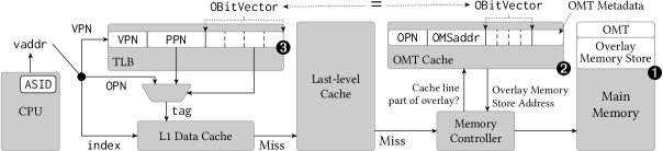
3.3.3 Microarchitecture and Memory Access Operations
Figure 3.5 depicts the details of our design. There are three main changes over the microarchitecture of current systems. First (➊ in the figure), main memory is split into two regions that store 1) regular physical pages and 2) the Overlay Memory Store (OMS). The OMS stores both a compact representation of the overlays and the Overlay Mapping Table (OMT), which maps each page from the Overlay Address Space to a location in the Overlay Memory Store. At a high level, each OMT entry contains 1) the OBitVector, indicating if each cache line within the corresponding page is present in the overlay, and 2) OMSaddr, the location of the overlay in the OMS. Second ➋, we augment the memory controller with a cache called the OMT Cache, which caches recently accessed entries from the OMT. Third ➌, because the TLB must determine if an access to a virtual address should be directed to the corresponding overlay, we extend each TLB entry to store the OBitVector. While this potentially increases the cost of each TLB miss (as it requires the OBitVector to be fetched from the OMT), our evaluations (Section 3.4) show that the performance benefit of using overlays more than offsets this additional TLB fill latency.
To describe the operation of different memory accesses, we use overlay-on-write (Section 3.1.2) as an example. Let us assume that two virtual pages (V1 and V2) are mapped to the same physical page in the copy-on-write mode, with a few cache lines of V2 already mapped to the overlay. There are three possible operations on V2: 1) a read, 2) a write to a cache line already in the overlay (simple write), and 3) a write to a cache line not present in the overlay (overlaying write). We now describe each of these operations in detail.
Memory Read Operation.
When the page V2 receives a read request, the processor first accesses the TLB with the corresponding page number (VPN) to retrieve the physical mapping (PPN) and the OBitVector. It generates the overlay page number (OPN) by concatenating the address space ID (ASID) of the process and the VPN (as described in Section 3.3.1). Depending on whether the accessed cache line is present in the overlay (as indicated by the corresponding bit in the OBitVector), the processor uses either the PPN or the OPN to generate the L1 cache tag. If the access misses in the entire cache hierarchy (L1 through last-level cache), the request is sent to the memory controller. The controller checks if the requested address is part of the overlay address space by checking the overlay bit in the physical address. If so, it looks up the overlay store address (OMSaddr) of the corresponding overlay page from the OMT Cache, and computes the exact location of the requested cache line within main memory (as described later in Section 3.3.4). It then accesses the cache line from the main memory and returns the data to the cache hierarchy.
Simple Write Operation.
When the processor receives a write to a cache line already present in the overlay, it simply has to update the cache line in the overlay. This operation is similar to a read operation, except the cache line is updated after it is read into the L1 cache.
Overlaying Write Operation.
An overlaying write operation is a write to a cache line that is not already present in the overlay. Since the virtual page is mapped to the regular physical page in the copy-on-write mode, the corresponding cache line must be remapped to the overlay (based on our semantics described in Section 3.1.2). We complete the overlaying write in three steps: 1) copy the data of the cache line in the regular physical page (PPN) to the corresponding cache line in the Overlay Address Space page (OPN), 2) update all the TLBs and the OMT to indicate that the cache line is mapped to the overlay, and 3) process the write operation.
The first step can be completed in hardware by reading the cache line from the regular physical page and simply updating the cache tag to correspond to the overlay page number (or by making an explicit copy of the cache line). Naïvely implementing the second step will involve a TLB shootdown for the corresponding virtual page. However, we exploit three simple facts to use the cache coherence network to keep the TLBs and the OMT coherent: i) the mapping is modified only for a single cache line, and not an entire page, ii) the overlay page address can be used to uniquely identify the virtual page since no overlay is shared between virtual pages, and iii) the overlay address is part of the physical address space and hence, part of the cache coherence network. Based on these facts, we propose a new cache coherence message called overlaying read exclusive. When a core receives this request, it checks if its TLB has cached the mapping for the virtual page. If so, the core simply sets the bit for the corresponding cache line in the OBitVector. The overlaying read exclusive request is also sent to the memory controller so that it can update the OBitVector of the corresponding overlay page in the OMT (via the OMT Cache). Once the remapping operation is complete, the write operation (the third step) is processed similar to the simple write operation.
Note that after an overlaying write, the corresponding cache line (which we will refer to as the overlay cache line) is marked dirty. However, unlike copy-on-write, which must allocate memory before the write operation, our mechanism allocates memory space lazily upon the eviction of the dirty overlay cache line – significantly improving performance.
Converting an Overlay to a Regular Physical Page.
Depending on the technique for which overlays are used, maintaining an overlay for a virtual page may be unnecessary after a point. For example, when using overlay-on-write, if most of the cache lines within a virtual page are modified, maintaining them in an overlay does not provide any advantage. The system may take one of three actions to promote an overlay to a physical page: The copy-and-commit action is one where the OS copies the data from the regular physical page to a new physical page and updates the data of the new physical page with the corresponding data from the overlay. The commit action updates the data of the regular physical page with the corresponding data from the overlay. The discard action simply discards the overlay.
While the copy-and-commit action is used with overlay-on-write, the commit and discard actions are used, for example, in the context of speculation, where our mechanism stores speculative updates in the overlays (Section 3.4.3). After any of these actions, the system clears the OBitVector of the corresponding virtual page, and frees the overlay memory store space allocated for the overlay (discussed next in Section 3.3.4).
3.3.4 Managing the Overlay Memory Store
The Overlay Memory Store (OMS) is the region in main memory where all the overlays are stored. As described in Section 3.3.3, the OMS is accessed only when an overlay access completely misses in the cache hierarchy. As a result, there are many simple ways to manage the OMS. One way is to have a small embedded core on the memory controller that can run a software routine that manages the OMS (similar mechanisms are supported in existing systems, e.g., Intel Active Management Technology [97]). Another approach is to let the memory controller manage the OMS by using a full physical page to store each overlay. While this approach will forgo the memory capacity benefit of our framework, it will still obtain the benefit of reducing overall work (Section 3.1.3).
In this section, we describe a hardware mechanism that obtains both the work reduction and the memory capacity reduction benefits of using overlays. In our mechanism, the controller fully manages the OMS with minimal interaction with the OS. Managing the OMS has two aspects. First, because each overlay contains only a subset of cache lines from the virtual page, we need a compact representation for the overlay, such that the OMS contains only cache lines that are actually present in the overlay. Second, the memory controller must manage multiple overlays of different sizes. We need a mechanism to handle such different sizes and the associated free space fragmentation issues. Although operations that allocate new overlays or relocate existing overlays are slightly complex, they are triggered only when a dirty overlay cache line is written back to main memory. Therefore, these operations are rare and are not on the critical path of execution.
Compact Overlay Representation.
One approach to compactly maintain the overlays is to store the cache lines in an overlay in the order in which they appear in the virtual page. While this representation is simple, if a new cache line is inserted into the overlay before other overlay cache lines, then the memory controller must move such cache lines to create a slot for the inserted line. This is a read-modify-write operation, which results in significant performance overhead.
We propose an alternative mechanism, in which each overlay is assigned a segment in the OMS. The overlay is associated with an array of pointers—one pointer for each cache line in the virtual page. Each pointer either points to the slot within the overlay segment that contains the cache line or is invalid if the cache line is not present in the overlay. We store this metadata in a single cache line at the head of the segment. For segments less than 4KB size, we use 64 5-bit slot pointers and a 32-bit vector indicating the free slots within a segment—total of 352 bits. For a 4KB segment, we do not store any metadata and simply store each overlay cache line at an offset which is same as the offset of the cache line within the virtual page. Figure 3.6 shows an overlay segment of size 256B, with only the first and the fourth cache lines of the virtual page mapped to the overlay.
Managing Multiple Overlay Sizes.
Different virtual pages may contain overlays of different sizes. The memory controller must store them efficiently in the available space. To simplify this management, our mechanism splits the available overlay space into segments of 5 fixed sizes: 256B, 512B, 1KB, 2KB, and 4KB. Each overlay is stored in the smallest segment that is large enough to store the overlay cache lines. When the memory controller requires a segment for a new overlay or when it wants to migrate an existing overlay to a larger segment, the controller identifies a free segment of the required size and updates the OMSaddr of the corresponding overlay page with the base address of the new segment. Individual cache lines are allocated their slots within the segment as and when they are written back to main memory.
Free Space Management.
To manage the free segments within the Overlay Memory Store, we use a simple linked-list based approach. For each segment size, the memory controller maintains a memory location or register that points to a free segment of that size. Each free segment in turn stores a pointer to another free segment of the same size or an invalid pointer denoting the end of the list. If the controller runs out of free segments of a particular size, it obtains a free segment of the next higher size and splits it into two. If the controller runs out of free 4KB segments, it requests the OS for an additional set of 4KB pages. During system startup, the OS proactively allocates a chunk of free pages to the memory controller. To reduce the number of memory operations needed to manage free segments, we use a grouped-linked-list mechanism, similar to the one used by some file systems [201].
The Overlay Mapping Table (OMT) and the OMT Cache.
The OMT maps pages from the Overlay Address Space to a specific segment in the Overlay Memory Store. For each page in the Overlay Address Space (i.e., for each OPN), the OMT contains an entry with the following pieces of information: 1) the OBitVector, indicating which cache lines are present in the overlay, and 2) the Overlay Memory Store Address (OMSaddr), pointing to the segment that stores the overlay. To reduce the storage cost of the OMT, we store it hierarchically, similar to the virtual-to-physical mapping tables. The memory controller maintains the root address of the hierarchical table in a register.
The OMT Cache stores the following details regarding recently-accessed overlays: the OBitVector, the OMSaddr, and the overlay segment metadata (stored at the beginning of the segment). To access a cache line from an overlay, the memory controller consults the OMT Cache with the overlay page number (OPN). In case of a hit, the controller acquires the necessary information to locate the cache line in the overlay memory store using the overlay segment metadata. In case of a miss, the controller performs an OMT walk (similar to a page table walk) to look up the corresponding OMT entry, and inserts it in the OMT Cache. It also reads the overlay segment metadata and caches it in the OMT cache entry. The controller may modify entries of the OMT, as and when overlays are updated. When such a modified entry is evicted from the OMT Cache, the memory controller updates the corresponding OMT entry in memory.
3.4 Applications and Evaluations
We describe seven techniques enabled by our framework, and quantitatively evaluate two of them. For our evaluations, we use memsim [16], an event-driven multi-core simulator that models out-of-order cores coupled with a DDR3-1066 [110] DRAM simulator. All the simulated systems use a three-level cache hierarchy with a uniform 64B cache line size. We do not enforce inclusion in any level of the hierarchy. We use the state-of-the-art DRRIP cache replacement policy [106] for the last-level cache. All our evaluated systems use an aggressive multi-stream prefetcher [205] similar to the one implemented in IBM Power 6 [131]. Table 3.1 lists the main configuration parameters in detail.
| Processor | 2.67 GHz, single issue, out-of-order, 64 entry instruction window, 64B cache lines |
|---|---|
| TLB | 4K pages, 64-entry 4-way associative L1 (1 cycle), 1024-entry L2 (10 cycles), TLB miss = 1000 cycles |
| L1 Cache | 64KB, 4-way associative, tag/data latency = 1/2 cycles, parallel tag/data lookup, LRU policy |
| L2 Cache | 512KB, 8-way associative, tag/data latency = 2/8 cycles, parallel tag/data lookup, LRU policy |
| Prefetcher | Stream prefetcher [131, 205], monitor L2 misses and prefetch into L3, 16 entries, degree = 4, distance = 24 |
| L3 Cache | 2MB, 16-way associative, tag/data latency = 10/24 cycles, serial tag/data lookup, DRRIP [106] policy |
| DRAM Controller | Open row, FR-FCFS drain when full [133], 64-entry write buffer, 64-entry OMT cache, miss latency = 1000 cycles |
| DRAM and Bus | DDR3-1066 MHz [110], 1 channel, 1 rank, 8 banks, 8B-wide data bus, burst length = 8, 8KB row buffer |
3.4.1 Overlay-on-write
As discussed in Section 3.1.2, overlay-on-write is a more efficient version of copy-on-write [79]: when multiple virtual pages share the same physical page in the copy-on-write mode and one of them receives a write, overlay-on-write simply moves the corresponding cache line to the overlay and updates the cache line in the overlay.
We compare the performance of overlay-on-write with that of copy-on-write using the fork [79] system call. fork is a widely-used system call with a number of different applications including creating new processes, creating stateful threads in multi-threaded applications, process testing/debugging [206, 53, 52], and OS speculation [234, 44, 162]. Despite its wide applications, fork is one of the most expensive system calls [186]. When invoked, fork creates a child process with an identical virtual address space as the calling process. fork marks all the pages of both processes as copy-on-write. As a result, when any such page receives a write, the copy-on-write mechanism must copy the whole page and remap the virtual page before it can proceed with the write.
Our evaluation models a scenario where a process is checkpointed at regular intervals using the fork system call. While we can test the performance of fork with any application, we use a subset of benchmarks from the SPEC CPU2006 benchmark suite [55]. Because the number of pages copied depends on the write working set of the application, we pick benchmarks with three different types of write working sets: 1) benchmarks with low write working set size, 2) benchmarks for which almost all cache lines within each modified page are updated, and 3) benchmarks for which only a few cache line within each modified page are updated. We pick five benchmarks for each type. For each benchmark, we fast forward the execution to its representative portion (determined using Simpoint [199]), run the benchmark for 200 million instructions (to warm up the caches), and execute a fork. After the fork, we run the parent process for another 300 million instructions, while the child process idles.222While 300 million instructions might seem low, several prior works (e.g., [53, 52]) argue for even shorter checkpoint intervals (10-100 million instructions).
Figure 3.8 plots the amount of additional memory consumed by the parent process using copy-on-write and overlay-on-write for the 300 million instructions after the fork. Figure 3.8 plots the performance (cycles per instruction) of the two mechanisms during the same period. We group benchmarks based on their type. We draw three conclusions.
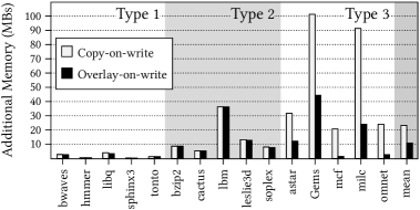
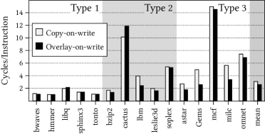
First, benchmarks with low write working set (Type 1) consume very little additional memory after forking (Figure 3.8). As a result, there is not much difference in the performance of copy-on-write and that of overlay-on-write (Figure 3.8).
Second, for benchmarks of Type 2, both mechanisms consume almost the same amount of additional memory. This is because for these benchmarks, almost all cache lines within every modified page are updated. However, with the exception of cactus, overlay-on-write significantly improves performance for this type of applications. Our analysis shows that the performance trends can be explained by the distance in time when cache lines of each page are updated by the application. When writes to different cache lines within a page are close in time, copy-on-write performs better than overlay-on-write. This is because copy-on-write fetches all the blocks of a page with high memory-level parallelism. On the other hand, when writes to different cache lines within a page are well separated in time, copy-on-write may 1) unnecessarily pollute the L1 cache with all the cache lines of the copied page, and 2) increase write bandwidth by generating two writes for each updated cache line (once when it is copied and again when the application updates the cache line). Overlay-on-write has neither of these drawbacks, and hence significantly improves performance over copy-on-write.
Third, for benchmarks of Type 3, overlay-on-write significantly reduces the amount of additional memory consumed compared to copy-on-write. This is because the write working set of these applications are spread out in the virtual address space, and copy-on-write unnecessarily copies cache lines that are actually not updated by the application. Consequently, overlay-on-write significantly improves performance compared to copy-on-write for this type of applications.
In summary, overlay-on-write reduces additional memory capacity requirements by 53% and improves performance by 15% compared to copy-on-write. Given the wide applicability of the fork system call, and the copy-on-write technique in general, we believe overlay-on-write can significantly benefit a variety of such applications.
3.4.2 Representing Sparse Data Structures
A sparse data structure is one with a significant fraction of zero values, e.g., a sparse matrix. Since only non-zero values typically contribute to computation, prior work developed many software representations for sparse data structures (e.g., [64, 100]). One popular representation of a sparse matrix is the Compressed Sparse Row (CSR) format [100]. To represent a sparse matrix, CSR stores only the non-zero values in an array, and uses two arrays of index pointers to identify the location of each non-zero value within the matrix.
While CSR efficiently stores sparse matrices, the additional index pointers maintained by CSR can result in inefficiency. First, the index pointers lead to significant additional memory capacity overhead (roughly 1.5 times the number of non-zero values in our evaluation—each value is 8 bytes, and each index pointer is 4 bytes). Second, any computation on the sparse matrix requires additional memory accesses to fetch the index pointers, which degrades performance.
Our framework enables a very efficient hardware-based representation for a sparse data structure: all virtual pages of the data structure map to a zero physical page and each virtual page is mapped to an overlay that contains only the non-zero cache lines from that page. To avoid computation over zero cache lines, we propose a new computation model that enables the software to perform computation only on overlays. When overlays are used to represent sparse data structures, this model enables the hardware to efficiently perform a computation only on non-zero cache lines. Because the hardware is aware of the overlay organization, it can efficiently prefetch the overlay cache lines and hide the latency of memory accesses significantly.
Our representation stores non-zero data at a cache line granularity. Hence, the performance and memory capacity benefits of our representation over CSR depends on the spatial locality of non-zero values within a cache line. To aid our analysis, we define a metric called non-zero value locality (), as the average number of non-zero values in each non-zero cache line. On the one hand, when non-zero values have poor locality ( 1), our representation will have to store a significant number of zero values and perform redundant computation over such values, degrading both memory capacity and performance over CSR, which stores and performs computation on only non-zero values. On the other hand, when non-zero values have high locality ( 8—e.g., each cache line stores 8 double-precision floating point values), our representation is significantly more efficient than CSR as it stores significantly less metadata about non-zero values than CSR. As a result, it outperforms CSR both in terms of memory capacity and performance.
We analyzed this trade-off using real-world sparse matrices of double-precision floating point values obtained from the UF Sparse Matrix Collection [58]. We considered all matrices with at least 1.5 million non-zero values (87 in total). Figure 3.9 plots the memory capacity and performance of one iteration of Sparse-Matrix Vector (SpMV) multiplication of our mechanism normalized to CSR for each of these matrices. The x-axis is sorted in the increasing order of the -value of the matrices.
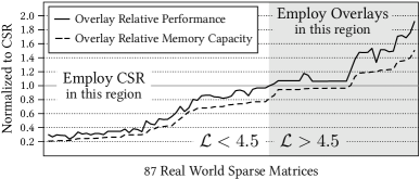
The trends can be explained by looking at the extreme points. On the left extreme, we have a matrix with = 1.09 (poisson3Db), i.e., most non-zero cache lines have only one non-zero value. As a result, our representation consumes 4.83 times more memory capacity and degrades performance by 70% compared to CSR. On the other extreme is a matrix with = 8 (raefsky4), i.e., none of the non-zero cache lines have any zero value. As a result, our representation is more efficient, reducing memory capacity by 34%, and improving performance by 92% compared to CSR.
Our results indicate that even when a little more than half of the values in each non-zero cache line are non-zero ( > 4.5), overlays outperform CSR. For 34 of the 87 real-world matrices, overlays reduce memory capacity by 8% and improve performance by 27% on average compared to CSR.
In addition to the performance and memory capacity benefits, our representation has several other major advantages over CSR (or any other software format). First, CSR is typically helpful only when the data structure is very sparse. In contrast, our representation exploits a wider degree of sparsity in the data structure. In fact, our simulations using randomly-generated sparse matrices with varying levels of sparsity (0% to 100%) show that our representation outperforms the dense-matrix representation for all sparsity levels—the performance gap increases linearly with the fraction of zero cache lines in the matrix. Second, in our framework, dynamically inserting non-zero values into a sparse matrix is as simple as moving a cache line to the overlay. In contrast, CSR incur a high cost to insert non-zero values. Finally, our computation model enables the system to seamlessly use optimized dense matrix codes on top of our representation. CSR, on the other hand, requires programmers to rewrite algorithms to suit CSR.
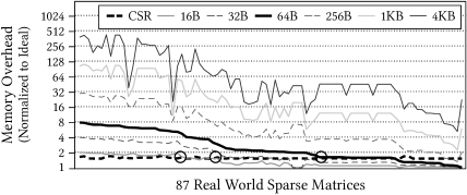
Sensitivity to Cache Line Size. So far, we have described the benefits of using overlays using 64B cache lines. However, one can imagine employing our approach at a 4KB page granularity (i.e., storing only non-zero pages as opposed to non-zero cache lines). To illustrate the benefits of fine-grained management, we compare the memory overhead of storing the sparse matrices using different cache line sizes (from 16B to 4KB). Figure 3.10 shows the results. The memory overhead for each cache line size is normalized to the ideal mechanism which stores only the non-zero values. The matrices are sorted in the same order as in Figure 3.9. We draw two conclusions from the figure. First, while storing only non-zero (4KB) pages may be a practical system to implement using today’s hardware, it increases the memory overhead by 53X on average. It would also increase the amount of computation, resulting in significant performance degradation. Hence, there is significant benefit to the fine-grained memory management enabled by overlays. Second, the results show that a mechanism using a finer granularity than 64B can outperform CSR on more matrices, indicating a direction for future research on sub-block management (e.g., [129]).
In summary, our overlay-based sparse matrix representation outperforms the state-of-the-art software representation on many real-world matrices, and consistently better than page-granularity management. We believe our approach has much wider applicability than existing representations.
3.4.3 Other Applications of Our Framework
We now describe five other applications that can be efficiently implemented on top of our framework. While prior works have already proposed mechanisms for some of these applications, our framework either enables a simpler mechanism or enables efficient hardware support for mechanisms proposed by prior work. We describe these mechanisms only at a high level, and defer more detailed explanations to future work.
Fine-grained Deduplication.
Gupta et al. [83] observe that in a system running multiple virtual machines with the same guest operating system, there are a number of pages that contain mostly same data. Their analysis shows that exploiting this redundancy can reduce memory capacity requirements by 50%. They propose the Difference Engine, which stores such similar pages using small patches over a common page. However, accessing such patched pages incurs significant overhead because the OS must apply the patch before retrieving the required data. Our framework enables a more efficient implementation of the Difference Engine wherein cache lines that are different from the base page can be stored in overlays, thereby enabling seamless access to patched pages, while also reducing the overall memory consumption. Compared to HICAMP [48], a cache line level deduplication mechanism that locates cache lines based on their content, our framework avoids significant changes to both the existing virtual memory framework and programming model.
Efficient Checkpointing.
Checkpointing is an important primitive in high performance computing applications where data structures are checkpointed at regular intervals to avoid restarting long-running applications from the beginning [63, 33, 230]. However, the frequency and latency of checkpoints are often limited by the amount of memory data that needs to be written to the backing store. With our framework, overlays could be used to capture all the updates between two checkpoints. Only these overlays need to be written to the backing store to take a new checkpoint, reducing the latency and bandwidth of checkpointing. The overlays are then committed (Section 3.3.3), so that each checkpoint captures precisely the delta since the last checkpoint. In contrast to prior works on efficient checkpointing such as INDRA [200], ReVive [174], and Sheaved Memory [207], our framework is more flexible than INDRA and ReVive (which are tied to recovery from remote attacks) and avoids the considerable write amplification of Sheaved Memory (which can significantly degrade overall system performance).
Virtualizing Speculation.
Several hardware-based speculative techniques (e.g., thread-level speculation [208, 203], transactional memory [54, 92]) have been proposed to improve system performance. Such techniques maintain speculative updates to memory in the cache. As a result, when a speculatively-updated cache line is evicted from the cache, these techniques must necessarily declare the speculation as unsuccessful, resulting in a potentially wasted opportunity. In our framework, these techniques can store speculative updates to a virtual page in the corresponding overlay. The overlay can be committed or discarded based on whether the speculation succeeds or fails. This approach is not limited by cache capacity and enables potentially unbounded speculation [25].
Fine-grained Metadata Management.
Storing fine-grained (e.g., word granularity) metadata about data has several applications (e.g., memcheck, taintcheck [227], fine-grained protection [236], detecting lock violations [187]). Prior works (e.g., [249, 159, 236, 227]) have proposed frameworks to efficiently store and manipulate such metadata. However, these mechanisms require hardware support specific to storing and maintaining metadata. In contrast, with our framework, the system can potentially use overlays for each virtual page to store metadata for the virtual page instead of an alternate version of the data. In other words, the Overlay Address Space serves as shadow memory for the virtual address space. To access some piece of data, the application uses the regular load and store instructions. The system would need new metadata load and metadata store instructions to enable the application to access the metadata from the overlays.
Flexible Super-pages.
Many modern architectures support super-pages to reduce the number of TLB misses. In fact, a recent prior work [31] suggests that a single arbitrarily large super-page (direct segment) can significantly reduce TLB misses for large servers. Unfortunately, using super-pages reduces the flexibility for the operating system to manage memory and implement techniques like copy-on-write. For example, to our knowledge, there is no system that shares a super-page across two processes in the copy-on-write mode. This lack of flexibility introduces a trade-off between the benefit of using super-pages to reduce TLB misses and the benefit of using copy-on-write to reduce memory capacity requirements. Fortunately, with our framework, we can apply overlays at higher-level page table entries to enable the OS to manage super-pages at a finer granularity. In short, we envision a mechanism that divides a super-page into smaller segments (based on the number of bits available in the OBitVector), and allows the system to potentially remap a segment of the super-page to the overlays. For example, when a super-page shared between two processes receives a write, only the corresponding segment is copied and the corresponding bit in the OBitVector is set. This approach can similarly be used to have multiple protection domains within a super-page. Assuming only a few segments within a super-page will require overlays, this approach can still ensure low TLB misses while enabling more flexibility for the OS.
3.5 Summary
In this chapter, we introduced a new, simple framework that enables fine-grained memory management. Our framework augments virtual memory with a concept called overlays. Each virtual page can be mapped to both a physical page and an overlay. The overlay contains only a subset of cache lines from the virtual page, and cache lines that are present in the overlay are accessed from there. We show that our proposed framework, with its simple access semantics, enables several fine-grained memory management techniques, without significantly altering the existing VM framework. We quantitatively demonstrate the benefits of our framework with two applications: 1) overlay-on-write, an efficient alternative to copy-on-write, and 2) an efficient hardware representation of sparse data structures. Our evaluations show that our framework significantly improves performance and reduces memory capacity requirements for both applications (e.g., 15% performance improvement and 53% memory capacity reduction, on average, for fork over traditional copy-on-write). Finally, we discuss five other potential applications for the page overlays.
Chapter 4 Understanding DRAM
In the second component of this dissertation, we propose a series of techniques to improve the efficiency of certain key primitives by exploiting the DRAM architecture. In this chapter, we will describe the modern DRAM architecture and its implementation in full detail. While we focus our attention primarily on commodity DRAM design (i.e., the DDRx interface), most DRAM architectures use very similar design approaches and vary only in higher-level design choices. As a result, our mechanisms, which we describe in the subsequent chapters, can be easily extended to any DRAM architecture. We now describe the high-level organization of the memory system.
4.1 High-level Organization of the Memory System
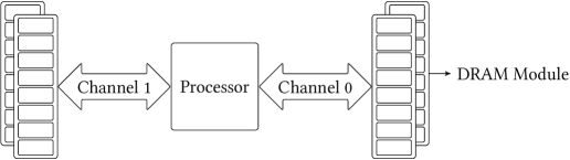
Figure 4.1 shows the organization of the memory subsystem in a modern system. At a high level, each processor chip consists of one of more off-chip memory channels. Each memory channel consists of its own set of command, address, and data buses. Depending on the design of the processor, there can be either an independent memory controller for each memory channel or a single memory controller for all memory channels. All modules connected to a channel share the buses of the channel. Each module consists of many DRAM devices (or chips). Most of this chapter (Section 4.2) is dedicated to describing the design of a modern DRAM chip. In Section 4.3, we present more details of the module organization of commodity DRAM.
4.2 DRAM Chip
A modern DRAM chip consists of a hierarchy of structures: DRAM cells, tiles/MATs, subarrays, and banks. In this section, we will describe the design of a modern DRAM chip in a bottom-up fashion, starting from a single DRAM cell and its operation.
4.2.1 DRAM Cell and Sense Amplifier
At the lowest level, DRAM technology uses capacitors to store information. Specifically, it uses the two extreme states of a capacitor, namely, the empty and the fully charged states to store a single bit of information. For instance, an empty capacitor can denote a logical value of 0, and a fully charged capacitor can denote a logical value of 1. Figure 4.2 shows the two extreme states of a capacitor.
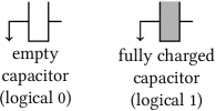
Unfortunately, the capacitors used for DRAM chips are small, and will get smaller with each new generation. As a result, the amount of charge that can be stored in the capacitor, and hence the difference between the two states is also very small. In addition, the capacitor can potentially lose its state after it is accessed. Therefore, to extract the state of the capacitor, DRAM manufactures use a component called sense amplifier.
Figure 4.4 shows a sense amplifier. A sense amplifier contains two inverters which are connected together such that the output of one inverter is connected to the input of the other and vice versa. The sense amplifier also has an enable signal that determines if the inverters are active. When enabled, the sense amplifier has two stable states, as shown in Figure 4.4. In both these stable states, each inverter takes a logical value and feeds the other inverter with the negated input.

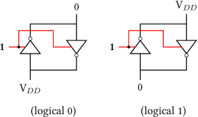
Figure 4.5 shows the operation of the sense amplifier from a disabled state. In the initial disabled state, we assume that the voltage level of the top terminal (Va) is higher than that of the bottom terminal (Vb). When the sense amplifier is enabled in this state, it senses the difference between the two terminals and amplifies the difference until it reaches one of the stable state (hence the name “sense amplifier”).
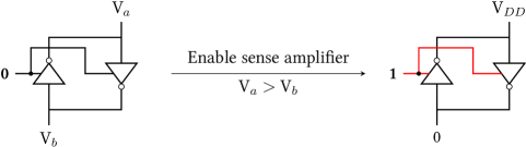
4.2.2 DRAM Cell Operation: The ACTIVATE-PRECHARGE cycle
DRAM technology uses a simple mechanism that converts the logical state of a capacitor into a logical state of the sense amplifier. Data can then be accessed from the sense amplifier (since it is in a stable state). Figure 4.6 shows the connection between a DRAM cell and the sense amplifier and the sequence of states involved in converting the cell state to the sense amplifier state.
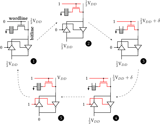
As shown in the figure (state ➊), the capacitor is connected to an access transistor that acts as a switch between the capacitor and the sense amplifier. The transistor is controller by a wire called wordline. The wire that connects the transistor to the top end of the sense amplifier is called bitline. In the initial state ➊, the wordline is lowered, the sense amplifier is disabled and both ends of the sense amplifier are maintained at a voltage level of VDD. We assume that the capacitor is initially fully charged (the operation is similar if the capacitor was empty). This state is referred to as the precharged state. An access to the cell is triggered by a command called ACTIVATE. Upon receiving an ACTIVATE, the corresponding wordline is first raised (state ➋). This connects the capacitor to the bitline. In the ensuing phase called charge sharing (state ➌), charge flows from the capacitor to the bitline, raising the voltage level on the bitline (top end of the sense amplifier) to V. After charge sharing, the sense amplifier is enabled (state ➍). The sense amplifier detects the difference in voltage levels between its two ends and amplifies the deviation, till it reaches the stable state where the top end is at VDD (state ➎). Since the capacitor is still connected to the bitline, the charge on the capacitor is also fully restored. We will shortly describe how the data can be accessed form the sense amplifier. However, once the access to the cell is complete, it is taken back to the original precharged state using the command called PRECHARGE. Upon receiving a PRECHARGE, the wordline is first lowered, thereby disconnecting the cell from the sense amplifier. Then, the two ends of the sense amplifier are driven to VDD using a precharge unit (not shown in the figure for brevity).
4.2.3 DRAM MAT/Tile: The Open Bitline Architecture
The goal of DRAM manufacturers is to maximize the density of the DRAM chips while adhering to certain latency constraints (described in Section 4.2.6). There are two costly components in the setup described in the previous section. The first component is the sense amplifier itself. Each sense amplifier is around two orders of magnitude larger than a single DRAM cell [178]. Second, the state of the wordline is a function of the address that is currently being accessed. The logic that is necessary to implement this function (for each cell) is expensive.
In order to reduce the overall cost of these two components, they are shared by many DRAM cells. Specifically, each sense amplifier is shared a column of DRAM cells. In other words, all the cells in a single column are connected to the same bitline. Similarly, each wordline is shared by a row of DRAM cells. Together, this organization consists of a 2-D array of DRAM cells connected to a row of sense amplifiers and a column of wordline drivers. Figure 4.7 shows this organization with a 2-D array.

To further reduce the overall cost of the sense amplifiers and the wordline driver, modern DRAM chips use an architecture called the open bitline architecture. This architecture exploits two observations. First, the sense amplifier is wider than the DRAM cells. This difference in width results in a white space near each column of cells. Second, the sense amplifier is symmetric. Therefore, cells can also be connected to the bottom part of the sense amplifier. Putting together these two observations, we can pack twice as many cells in the same area using the open bitline architecture, as shown in Figure 4.8;

As shown in the figure, a 2-D array of DRAM cells is connected to two rows of sense amplifiers: one on the top and one on the bottom of the array. While all the cells in a given row share a common wordline, half the cells in each row are connected to the top row of sense amplifiers and the remaining half of the cells are connected to the bottom row of sense amplifiers. This tightly packed structure is called a DRAM MAT/Tile [224, 246, 125]. In a modern DRAM chip, each MAT typically is a or array. Multiple MATs are grouped together to form a larger structure called a DRAM bank, which we describe next.
4.2.4 DRAM Bank
In most commodity DRAM interfaces [110, 111], a DRAM bank is the smallest structure visible to the memory controller. All commands related to data access are directed to a specific bank. Logically, each DRAM bank is a large monolithic structure with a 2-D array of DRAM cells connected to a single set of sense amplifiers (also referred to as a row buffer). For example, in a 2Gb DRAM chip with 8 banks, each bank has rows and each logical row has 8192 DRAM cells. Figure 4.9 shows this logical view of a bank.
In addition to the MAT, the array of sense amplifiers, and the wordline driver, each bank also consists of some peripheral structures to decode DRAM commands and addresses, and manage the input/output to the DRAM bank. Specifically, each bank has a row decoder to decode the row address of row-level commands (e.g., ACTIVATE). Each data access command (READ and WRITE) accesses only a part of a DRAM row. Such individual parts are referred to as columns. With each data access command, the address of the column to be accessed is provided. This address is decoded by the column selection logic. Depending on which column is selected, the corresponding piece of data is communicated between the sense amplifiers and the bank I/O logic. The bank I/O logic intern acts as an interface between the DRAM bank and the chip-level I/O logic.
Although the bank can logically be viewed as a single MAT, building a single MAT of a very large dimension is practically not feasible as it will require very long bitlines and wordlines. Therefore, each bank is physically implemented as a 2-D array of DRAM MATs. Figure 4.10 shows a physical implementation of the DRAM bank with 4 MATs arranged in array. As shown in the figure, the output of the global row decoder is sent to each row of MATs. The bank I/O logic, also known as the global sense amplifiers, are connected to all the MATs through a set of global bitlines. As shown in the figure, each vertical collection of MATs consists of its own columns selection logic and global bitlines. One implication of this division is that the data accessed by any command is split equally across all the MATs in a single row of MATs.
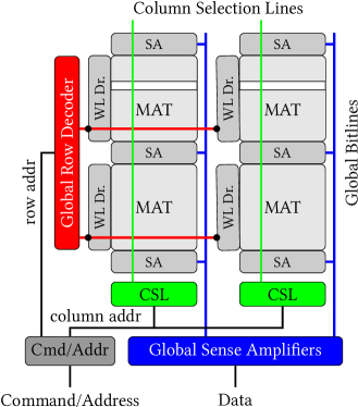
Figure 4.11 shows the zoomed-in version of a DRAM MAT with the surrounding peripheral logic. Specifically, the figure shows how each column selection line selects specific sense amplifiers from a MAT and connects them to the global bitlines. It should be noted that the width of the global bitlines for each MAT (typically 8/16) is much smaller than that of the width of the MAT (typically 512/1024).
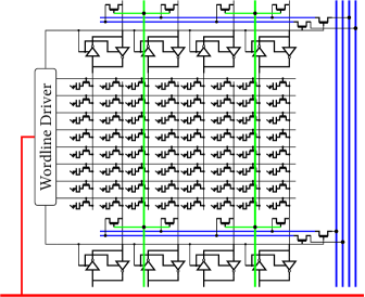
Each DRAM chip consist of multiple banks as shown in Figure 4.12. All the banks share the chip’s internal command, address, and data buses. As mentioned before, each bank operates mostly independently (except for operations that involve the shared buses). The chip I/O manages the transfer of data to and from the chip’s internal bus to the channel. The width of the chip output (typically 8 bits) is much smaller than the output width of each bank (typically 64 bits). Any piece of data accessed from a DRAM bank is first buffered at the chip I/O and sent out on the memory bus 8 bits at a time. With the DDR (double data rate) technology, 8 bits are sent out each half cycle. Therefore, it takes 4 cycles to transfer 64 bits of data from a DRAM chip I/O on to the memory channel.
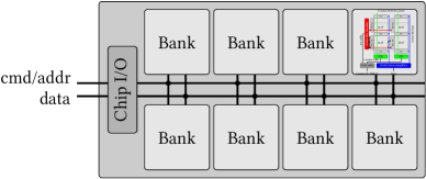
4.2.5 DRAM Commands: Accessing Data from a DRAM Chip
To access a piece of data from a DRAM chip, the memory controller must first identify the location of the data: the bank ID (), the row address () within the bank, and the column address () within the row. After identifying these pieces of information, accessing the data involves three steps.
The first step is to issue a PRECHARGE to the bank . This step prepares the bank for a data access by ensuring that all the sense amplifiers are in the precharged state (Figure 4.6, state ➊). No wordline within the bank is raised in this state.
The second step is to activate the row that contains the data. This step is triggered by issuing a ACTIVATE to bank with row address . Upon receiving this command, the corresponding bank feeds its global row decoder with the input . The global row decoder logic then raises the wordline of the DRAM row corresponding to the address and enables the sense amplifiers connected to that row. This triggers the DRAM cell operation described in Section 4.2.2. At the end of the activate operation the data from the entire row of DRAM cells is copied to the corresponding array of sense amplifiers.
Finally, the third step is to access the data from the required column. This is done by issuing a READ or WRITE command to the bank with the column address . Upon receiving a READ or WRITE command, the corresponding address is fed to the column selection logic. The column selection logic then raises the column selection lines (Figure 4.11) corresponding the address , thereby connecting those sense amplifiers to the global sense amplifiers through the global bitlines. For a read access, the global sense amplifiers sense the data from the MAT’s local sense amplifiers and transfer that data to chip’s internal bus. For a write access, the global sense amplifiers read the data from the chip’s internal bus and force the MAT’s local sense amplifiers to the appropriate state.
Not all data accesses require all three steps. Specifically, if the row to be accessed is already activated in the corresponding bank, then the first two steps can be skipped and the data can be directly accessed by issuing a READ or WRITE to the bank. For this reason, the array of sense amplifiers are also referred to as a row buffer, and such an access that skips the first two steps is called a row buffer hit. Similarly, if the bank is already in the precharged state, then the first step can be skipped. Such an access is referred to as a row buffer miss. Finally, if a different row is activated within the bank, then all three steps have to be performed. Such a situation is referred to as a row buffer conflict.
4.2.6 DRAM Timing Constraints
Different operations within DRAM consume different amounts of time. Therefore, after issuing a command, the memory controller must wait for a sufficient amount of time before it can issue the next command. Such wait times are managed by what are called the timing constraints. Timing constraints essentially dictate the minimum amount of time between two commands issued to the same bank/rank/channel. Table 4.1 describes some key timing constraints along with their values for the DDR3-1600 interface.
| Name | Constraint | Description | Value (ns) | ||
|---|---|---|---|---|---|
| tRAS | ACTIVATE | PRECHARGE | Time taken to complete a row activation operation in a bank | 35 | |
| tRCD | ACTIVATE | READ/WRITE | Time between an activate command and column command to a bank | 15 | |
| tRP | PRECHARGE | ACTIVATE | Time taken to complete a precharge operation in a bank | 15 | |
| tWR | WRITE | PRECHARGE | Time taken to ensure that data is safely written to the DRAM cells after a write operation (write recovery) | 15 | |
4.3 DRAM Module
As mentioned before, each READ or WRITE command for a single DRAM chip typically involves only 64 bits. In order to achieve high memory bandwidth, commodity DRAM modules group several DRAM chips (typically 4 or 8) together to form a rank of DRAM chips. The idea is to connect all chips of a single rank to the same command and address buses, while providing each chip with an independent data bus. In effect, all the chips within a rank receive the same commands with same addresses, making the rank a logically wide DRAM chip. Figure 4.13 shows the logical organization of a DRAM rank.
Most commodity DRAM ranks consist of 8 chips. Therefore, each READ or WRITE command accesses 64 bytes of data, the typical cache line size in most processors.
4.4 Summary
In this section, we summarize the key takeaways of the DRAM design and operation.
-
1.
To access data from a DRAM cell, DRAM converts the state of the cell into one of the stable states of the sense amplifier. The precharged state of the sense amplifier, wherein both the bitline and the are charged to a voltage level of VDD, is key to this state transfer, as the DRAM cell is large enough to perturb the voltage level on the bitline.
-
2.
The DRAM cell is not strong enough to switch the sense amplifier from one stable state to another. If a cell is connected to a stable sense amplifier, the charge on the cell gets overwritten to reflect the state of the sense amplifier.
-
3.
In the DRAM cell operation, the final state of the sense amplifier after the amplification phase depends solely on the deviation on the bitline after charge sharing. If the deviation is positive, the sense amplifier drives the bitline to VDD. Otherwise, if the deviation is negative, the sense amplifier drives the bitline to 0.
-
4.
In commodity DRAM, each ACTIVATE command simultaneously activates an entire row of DRAM cells. In a single chip, this typically corresponds to 8 Kbits of cells. Across a rank with 8 chips, each ACTIVATE activates 8 KB of data.
-
5.
In a commodity DRAM module, the data corresponding to each READ or WRITE is equally distributed across all the chips in a rank. All the chips share the same command and address bus, while each chip has an independent data bus.
All our mechanisms are built on top of these observations. We will recap these observations in the respective chapters.
Chapter 5 RowClone
Originally published as “RowClone: Fast and Energy-efficient In-DRAM Bulk Data Copy and Initialization” in the International Symposium on Microarchitecture, 2013 [192]
In Section 2.1.2, we described the source of inefficiency in performing a page copy operation in existing systems. Briefly, in existing systems, a page copy operation (or any bulk copy operation) is at best performed one cache line at a time. The operation requires a large number of cache lines to be transferred back and forth on the main memory channel. As a result, a bulk copy operation incurs high latency, high bandwidth consumption, and high energy consumption.
In this chapter, we present RowClone, a mechanism that can perform bulk copy and initialization operations completely inside DRAM. We show that this approach obviates the need to transfer large quantities of data on the memory channel, thereby significantly improving the efficiency of a bulk copy operation. As bulk data initialization (specifically bulk zeroing) can be viewed as a special case of a bulk copy operation, RowClone can be easily extended to perform such bulk initialization operations with high efficiency.
5.1 The RowClone DRAM Substrate
RowClone consists of two independent mechanisms that exploit several observations about DRAM organization and operation. Our first mechanism efficiently copies data between two rows of DRAM cells that share the same set of sense amplifiers (i.e., two rows within the same subarray). We call this mechanism the Fast Parallel Mode (FPM). Our second mechanism efficiently copies cache lines between two banks within a module in a pipelined manner. We call this mechanism the Piplines Serial Mode (PSM). Although not as fast as FPM, PSM has fewer constraints and hence is more generally applicable. We now describe these two mechanism in detail.
5.1.1 Fast-Parallel Mode
The Fast Parallel Mode (FPM) is based on the following three observations about DRAM.
-
1.
In a commodity DRAM module, each ACTIVATE command transfers data from a large number of DRAM cells (multiple kilo-bytes) to the corresponding array of sense amplifiers (Section 4.3).
-
2.
Several rows of DRAM cells share the same set of sense amplifiers (Section 4.2.3).
-
3.
A DRAM cell is not strong enough to flip the state of the sense amplifier from one stable state to another stable state. In other words, if a cell is connected to an already activated sense amplifier (or bitline), then the data of the cell gets overwritten with the data on the sense amplifier.
While the first two observations are direct implications from the design of commodity DRAM, the third observation exploits the fact that DRAM cells are large enough to cause only a small perturbation on the bitline voltage. Figure 5.1 pictorially shows how this observation can be used to copy data between two cells that share a sense amplifier.
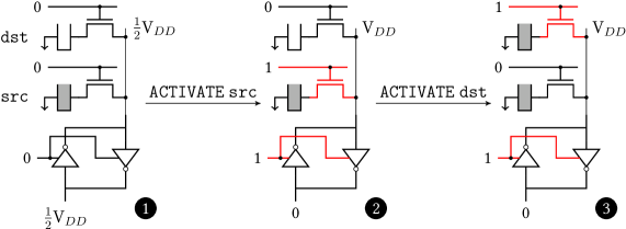
The figure shows two cells (src and dst) connected to a single sense amplifier. In the initial state, we assume that src is fully charged and dst is fully empty, and the sense amplifier is in the precharged state (➊). In this state, FPM issues an ACTIVATE to src. At the end of the activation operation, the sense amplifier moves to a stable state where the bitline is at a voltage level of VDD and the charge in src is fully restored (➋). FPM follows this operation with an ACTIVATE to dst, without an intervening PRECHARGE. This operation lowers the wordline corresponding to src and raises the wordline of dst, connecting dst to the bitline. Since the bitline is already fully activated, even though dst is initially empty, the perturbation caused by the cell is not sufficient to flip the state of the bitline. As a result, sense amplifier continues to drive the bitline to VDD, thereby pushing dst to a fully charged state (➌).
It can be shown that regardless of the initial state of src and dst, the above operation copies the data from src to dst. Given that each ACTIVATE operates on an entire row of DRAM cells, the above operation can copy multiple kilo bytes of data with just two back-to-back ACTIVATE operations.
Unfortunately, modern DRAM chips do not allow another ACTIVATE to an already activated bank – the expected result of such an action is undefined. This is because a modern DRAM chip allows at most one row (subarray) within each bank to be activated. If a bank that already has a row (subarray) activated receives an ACTIVATE to a different subarray, the currently activated subarray must first be precharged [125].111Some DRAM manufacturers design their chips to drop back-to-back ACTIVATEs to the same bank.
To support FPM, we propose the following change to the DRAM chip in the way it handles back-to-back ACTIVATEs. When an already activated bank receives an ACTIVATE to a row, the chip processes the command similar to any other ACTIVATE if and only if the command is to a row that belongs to the currently activated subarray. If the row does not belong to the currently activated subarray, then the chip takes the action it normally does with back-to-back ACTIVATEs—e.g., drop it. Since the logic to determine the subarray corresponding to a row address is already present in today’s chips, implementing FPM only requires a comparison to check if the row address of an ACTIVATE belongs to the currently activated subarray, the cost of which is almost negligible.
Summary. To copy data from src to dst within the same subarray, FPM first issues an ACTIVATE to src. This copies the data from src to the subarray row buffer. FPM then issues an ACTIVATE to dst. This modifies the input to the subarray row-decoder from src to dst and connects the cells of dst row to the row buffer. This, in effect, copies the data from the sense amplifiers to the destination row. As we show in Section 5.5.1, with these two steps, FPM copies a 4KB page of data 11.6x faster and with 74.4x less energy than an existing system.
Limitations. FPM has two constraints that limit its general applicability. First, it requires the source and destination rows to be within the same subarray (i.e., share the same set of sense amplifiers). Second, it cannot partially copy data from one row to another. Despite these limitations, we show that FPM can be immediately applied to today’s systems to accelerate two commonly used primitives in modern systems – Copy-on-Write and Bulk Zeroing (Section 7.3). In the following section, we describe the second mode of RowClone – the Pipelined Serial Mode (PSM). Although not as fast or energy-efficient as FPM, PSM addresses these two limitations of FPM.
5.1.2 Pipelined Serial Mode
The Pipelined Serial Mode efficiently copies data from a source row in one bank to a destination row in a different bank. PSM exploits the fact that a single internal bus that is shared across all the banks is used for both read and write operations. This enables the opportunity to copy an arbitrary quantity of data one cache line at a time from one bank to another in a pipelined manner.
To copy data from a source row in one bank to a destination row in a different bank, PSM first activates the corresponding rows in both banks. It then puts the source bank in the read mode, the destination bank in the write mode, and transfers data one cache line (corresponding to a column of data—64 bytes) at a time. For this purpose, we propose a new DRAM command called TRANSFER. The TRANSFER command takes four parameters: 1) source bank index, 2) source column index, 3) destination bank index, and 4) destination column index. It copies the cache line corresponding to the source column index in the activated row of the source bank to the cache line corresponding to the destination column index in the activated row of the destination bank.
Unlike READ/WRITE which interact with the memory channel connecting the processor and main memory, TRANSFER does not transfer data outside the chip. Figure 5.2 pictorially compares the operation of the TRANSFER command with that of READ and WRITE. The dashed lines indicate the data flow corresponding to the three commands. As shown in the figure, in contrast to the READ or WRITE commands, TRANSFER does not transfer data from or to the memory channel.
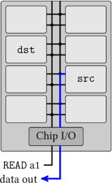
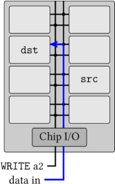
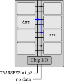
5.1.3 Mechanism for Bulk Data Copy
When the data from a source row (src) needs to be copied to a destination row (dst), there are three possible cases depending on the location of src and dst: 1) src and dst are within the same subarray, 2) src and dst are in different banks, 3) src and dst are in different subarrays within the same bank. For case 1 and case 2, RowClone uses FPM and PSM, respectively, to complete the operation (as described in Sections 5.1.1 and 5.1.2).
For the third case, when src and dst are in different subarrays within the same bank, one can imagine a mechanism that uses the global bitlines (shared across all subarrays within a bank – described in [125]) to copy data across the two rows in different subarrays. However, we do not employ such a mechanism for two reasons. First, it is not possible in today’s DRAM chips to activate multiple subarrays within the same bank simultaneously. Second, even if we enable simultaneous activation of multiple subarrays, as in [125], transferring data from one row buffer to another using the global bitlines requires the bank I/O circuitry to switch between read and write modes for each cache line transfer. This switching incurs significant latency overhead. To keep our design simple, for such an intra-bank copy operation, our mechanism uses PSM to first copy the data from src to a temporary row (tmp) in a different bank. It then uses PSM again to copy the data back from tmp to dst. The capacity lost due to reserving one row within each bank is negligible (0.0015% for a bank with 64k rows).
5.1.4 Mechanism for Bulk Data Initialization
Bulk data initialization sets a large block of memory to a specific value. To perform this operation efficiently, our mechanism first initializes a single DRAM row with the corresponding value. It then uses the appropriate copy mechanism (from Section 5.1.3) to copy the data to the other rows to be initialized.
Bulk Zeroing (or BuZ), a special case of bulk initialization, is a frequently occurring operation in today’s systems [113, 240]. To accelerate BuZ, one can reserve one row in each subarray that is always initialized to zero. By doing so, our mechanism can use FPM to efficiently BuZ any row in DRAM by copying data from the reserved zero row of the corresponding subarray into the destination row. The capacity loss of reserving one row out of 512 rows in each subarray is very modest (0.2%).
While the reserved rows can potentially lead to gaps in the physical address space, we can use an appropriate memory interleaving technique that maps consecutive rows to different subarrays. Such a technique ensures that the reserved zero rows are contiguously located in the physical address space. Note that interleaving techniques commonly used in today’s systems (e.g., row or cache line interleaving) have this property.
5.2 End-to-end System Design
So far, we described RowClone, a DRAM substrate that can efficiently perform bulk data copy and initialization. In this section, we describe the changes to the ISA, the processor microarchitecture, and the operating system that will enable the system to efficiently exploit the RowClone DRAM substrate.
5.2.1 ISA Support
To enable the software to communicate occurrences of bulk copy and initialization operations to the hardware, we introduce two new instructions to the ISA: memcopy and meminit. Table 5.1 describes the semantics of these two new instructions. We deliberately keep the semantics of the instructions simple in order to relieve the software from worrying about microarchitectural aspects of RowClone such as row size, alignment, etc. (discussed in Section 5.2.2). Note that such instructions are already present in some of the instructions sets in modern processors – e.g., rep movsd, rep stosb, ermsb in x86 [101] and mvcl in IBM S/390 [96].
| Instruction | Operands | Semantics |
|---|---|---|
| memcopy | src, dst, size | Copy size bytes from src to dst |
| meminit | dst, size, val | Set size bytes to val at dst |
There are three points to note regarding the execution semantics of these operations. First, the processor does not guarantee atomicity for both memcopy and meminit, but note that existing systems also do not guarantee atomicity for such operations. Therefore, the software must take care of atomicity requirements using explicit synchronization. However, the microarchitectural implementation will ensure that any data in the on-chip caches is kept consistent during the execution of these operations (Section 5.2.2). Second, the processor will handle any page faults during the execution of these operations. Third, the processor can take interrupts during the execution of these operations.
5.2.2 Processor Microarchitecture Support
The microarchitectural implementation of the new instructions, memcopy and meminit, has two parts. The first part determines if a particular instance of memcopy or meminit can be fully/partially accelerated by RowClone. The second part involves the changes required to the cache coherence protocol to ensure coherence of data in the on-chip caches. We discuss these parts in this section.
Source/Destination Alignment and Size
For the processor to accelerate a copy/initialization operation using RowClone, the operation must satisfy certain alignment and size constraints. Specifically, for an operation to be accelerated by FPM, 1) the source and destination regions should be within the same subarray, 2) the source and destination regions should be row-aligned, and 3) the operation should span an entire row. On the other hand, for an operation to be accelerated by PSM, the source and destination regions should be cache line-aligned and the operation must span a full cache line.
Upon encountering a memcopy/meminit instruction, the processor divides the region to be copied/initialized into three portions: 1) row-aligned row-sized portions that can be accelerated using FPM, 2) cache line-aligned cache line-sized portions that can be accelerated using PSM, and 3) the remaining portions that can be performed by the processor. For the first two regions, the processor sends appropriate requests to the memory controller which completes the operations and sends an acknowledgment back to the processor. Since TRANSFER copies only a single cache line, a bulk copy using PSM can be interleaved with other commands to memory. The processor completes the operation for the third region similarly to how it is done in today’s systems. Note that the CPU can offload all these operations to the memory controller. In such a design, the CPU need not be made aware of the DRAM organization (e.g., row size and alignment, subarray mapping, etc.).
Managing On-Chip Cache Coherence
RowClone allows the memory controller to directly read/modify data in memory without going through the on-chip caches. Therefore, to ensure cache coherence, the controller appropriately handles cache lines from the source and destination regions that may be present in the caches before issuing the copy/initialization operations to memory.
First, the memory controller writes back any dirty cache line from the source region as the main memory version of such a cache line is likely stale. Copying the data in-memory before flushing such cache lines will lead to stale data being copied to the destination region. Second, the controller invalidates any cache line (clean or dirty) from the destination region that is cached in the on-chip caches. This is because after performing the copy operation, the cached version of these blocks may contain stale data. The controller already has the ability to perform such flushes and invalidations to support Direct Memory Access (DMA) [102]. After performing the necessary flushes and invalidations, the memory controller performs the copy/initialization operation. To ensure that cache lines of the destination region are not cached again by the processor in the meantime, the memory controller blocks all requests (including prefetches) to the destination region until the copy or initialization operation is complete.
While performing the flushes and invalidates as mentioned above will ensure coherence, we propose a modified solution to handle dirty cache lines of the source region to reduce memory bandwidth consumption. When the memory controller identifies a dirty cache line belonging to the source region while performing a copy, it creates an in-cache copy of the source cache line with the tag corresponding to the destination cache line. This has two benefits. First, it avoids the additional memory flush required for the dirty source cache line. Second and more importantly, the controller does not have to wait for all the dirty source cache lines to be flushed before it can perform the copy. In Section 5.5.3, we will consider another optimization, called RowClone-Zero-Insert, which inserts clean zero cache lines into the cache to further optimize Bulk Zeroing. This optimization does not require further changes to our proposed modifications to the cache coherence protocol.
Although RowClone requires the controller to manage cache coherence, it does not affect memory consistency — i.e., concurrent readers or writers to the source or destination regions involved in a bulk copy or initialization operation. As mentioned before, such an operation is not guaranteed to be atomic even in current systems, and the software needs to perform the operation within a critical section to ensure atomicity.
5.2.3 Software Support
The minimum support required from the system software is the use of the proposed memcopy and meminit instructions to indicate bulk data operations to the processor. Although one can have a working system with just this support, maximum latency and energy benefits can be obtained if the hardware is able to accelerate most copy operations using FPM rather than PSM. Increasing the likelihood of the use of the FPM mode requires further support from the operating system (OS) on two aspects: 1) page mapping, and 2) granularity of copy/initialization.
Subarray-Aware Page Mapping
The use of FPM requires the source row and the destination row of a copy operation to be within the same subarray. Therefore, to maximize the use of FPM, the OS page mapping algorithm should be aware of subarrays so that it can allocate a destination page of a copy operation in the same subarray as the source page. More specifically, the OS should have knowledge of which pages map to the same subarray in DRAM. We propose that DRAM expose this information to software using the small EEPROM that already exists in today’s DRAM modules. This EEPROM, called the Serial Presence Detect (SPD) [109], stores information about the DRAM chips that is read by the memory controller at system bootup. Exposing the subarray mapping information will require only a few additional bytes to communicate the bits of the physical address that map to the subarray index.222To increase DRAM yield, DRAM manufacturers design chips with spare rows that can be mapped to faulty rows [94]. Our mechanism can work with this technique by either requiring that each faulty row is remapped to a spare row within the same subarray, or exposing the location of all faulty rows to the memory controller so that it can use PSM to copy data across such rows.
Once the OS has the mapping information between physical pages and subarrays, it maintains multiple pools of free pages, one pool for each subarray. When the OS allocates the destination page for a copy operation (e.g., for a Copy-on-Write operation), it chooses the page from the same pool (subarray) as the source page. Note that this approach does not require contiguous pages to be placed within the same subarray. As mentioned before, commonly used memory interleaving techniques spread out contiguous pages across as many banks/subarrays as possible to improve parallelism. Therefore, both the source and destination of a bulk copy operation can be spread out across many subarrays.
Granularity of Copy/Initialization
The second aspect that affects the use of FPM is the granularity at which data is copied or initialized. FPM has a minimum granularity at which it can copy or initialize data. There are two factors that affect this minimum granularity: 1) the size of each DRAM row, and 2) the memory interleaving employed by the controller.
First, FPM copies all the data of the source row to the destination row (across the entire DIMM). Therefore, the minimum granularity of copy using FPM is at least the size of the row. Second, to extract maximum bandwidth, some memory interleaving techniques map consecutive cache lines to different memory channels in the system. Therefore, to copy/initialize a contiguous region of data with such interleaving strategies, FPM must perform the copy operation in each channel. The minimum amount of data copied by FPM in such a scenario is the product of the row size and the number of channels.
To maximize the likelihood of using FPM, the system or application software must ensure that the region of data copied (initialized) using the memcopy (meminit) instructions is at least as large as this minimum granularity. For this purpose, we propose to expose this minimum granularity to the software through a special register, which we call the Minimum Copy Granularity Register (MCGR). On system bootup, the memory controller initializes the MCGR based on the row size and the memory interleaving strategy, which can later be used by the OS for effectively exploiting RowClone. Note that some previously proposed techniques such as sub-wordline activation [224] or mini-rank [231, 252] can be combined with RowClone to reduce the minimum copy granularity, further increasing the opportunity to use FPM.
5.3 Applications
RowClone can be used to accelerate any bulk copy and initialization operation to improve both system performance and energy efficiency. In this paper, we quantitatively evaluate the efficacy of RowClone by using it to accelerate two primitives widely used by modern system software: 1) Copy-on-Write and 2) Bulk Zeroing. We now describe these primitives followed by several applications that frequently trigger them.
5.3.1 Primitives Accelerated by RowClone
Copy-on-Write (CoW) is a technique used by most modern operating systems (OS) to postpone an expensive copy operation until it is actually needed. When data of one virtual page needs to be copied to another, instead of creating a copy, the OS points both virtual pages to the same physical page (source) and marks the page as read-only. In the future, when one of the sharers attempts to write to the page, the OS allocates a new physical page (destination) for the writer and copies the contents of the source page to the newly allocated page. Fortunately, prior to allocating the destination page, the OS already knows the location of the source physical page. Therefore, it can ensure that the destination is allocated in the same subarray as the source, thereby enabling the processor to use FPM to perform the copy.
Bulk Zeroing (BuZ) is an operation where a large block of memory is zeroed out. As mentioned in Section 5.1.4, our mechanism maintains a reserved row that is fully initialized to zero in each subarray. For each row in the destination region to be zeroed out, the processor uses FPM to copy the data from the reserved zero-row of the corresponding subarray to the destination row.
5.3.2 Applications that Use CoW/BuZ
We now describe seven example applications or use-cases that extensively use the CoW or BuZ operations. Note that these are just a small number of example scenarios that incur a large number of copy and initialization operations.
Process Forking. fork is a frequently-used system call in modern operating systems (OS). When a process (parent) calls fork, it creates a new process (child) with the exact same memory image and execution state as the parent. This semantics of fork makes it useful for different scenarios. Common uses of the fork system call are to 1) create new processes, and 2) create stateful threads from a single parent thread in multi-threaded programs. One main limitation of fork is that it results in a CoW operation whenever the child/parent updates a shared page. Hence, despite its wide usage, as a result of the large number of copy operations triggered by fork, it remains one of the most expensive system calls in terms of memory performance [186].
Initializing Large Data Structures. Initializing large data structures often triggers Bulk Zeroing. In fact, many managed languages (e.g., C#, Java, PHP) require zero initialization of variables to ensure memory safety [240]. In such cases, to reduce the overhead of zeroing, memory is zeroed-out in bulk.
Secure Deallocation. Most operating systems (e.g., Linux [36], Windows [185], Mac OS X [202]) zero out pages newly allocated to a process. This is done to prevent malicious processes from gaining access to the data that previously belonged to other processes or the kernel itself. Not doing so can potentially lead to security vulnerabilities, as shown by prior works [50, 62, 85, 87].
Process Checkpointing. Checkpointing is an operation during which a consistent version of a process state is backed-up, so that the process can be restored from that state in the future. This checkpoint-restore primitive is useful in many cases including high-performance computing servers [33], software debugging with reduced overhead [206], hardware-level fault and bug tolerance mechanisms [53, 52], and speculative OS optimizations to improve performance [44, 234]. However, to ensure that the checkpoint is consistent (i.e., the original process does not update data while the checkpointing is in progress), the pages of the process are marked with copy-on-write. As a result, checkpointing often results in a large number of CoW operations.
Virtual Machine Cloning/Deduplication. Virtual machine (VM) cloning [130] is a technique to significantly reduce the startup cost of VMs in a cloud computing server. Similarly, deduplication is a technique employed by modern hypervisors [229] to reduce the overall memory capacity requirements of VMs. With this technique, different VMs share physical pages that contain the same data. Similar to forking, both these operations likely result in a large number of CoW operations for pages shared across VMs.
Page Migration. Bank conflicts, i.e., concurrent requests to different rows within the same bank, typically result in reduced row buffer hit rate and hence degrade both system performance and energy efficiency. Prior work [217] proposed techniques to mitigate bank conflicts using page migration. The PSM mode of RowClone can be used in conjunction with such techniques to 1) significantly reduce the migration latency and 2) make the migrations more energy-efficient.
CPU-GPU Communication. In many current and future processors, the GPU is or is expected to be integrated on the same chip with the CPU. Even in such systems where the CPU and GPU share the same off-chip memory, the off-chip memory is partitioned between the two devices. As a consequence, whenever a CPU program wants to offload some computation to the GPU, it has to copy all the necessary data from the CPU address space to the GPU address space [105]. When the GPU computation is finished, all the data needs to be copied back to the CPU address space. This copying involves a significant overhead. By spreading out the GPU address space over all subarrays and mapping the application data appropriately, RowClone can significantly speed up these copy operations. Note that communication between different processors and accelerators in a heterogeneous System-on-a-chip (SoC) is done similarly to the CPU-GPU communication and can also be accelerated by RowClone.
We now quantitatively compare RowClone to existing systems and show that RowClone significantly improves both system performance and energy efficiency.
5.4 Methodology
Simulation. Our evaluations use an in-house cycle-level multi-core simulator along with a cycle-accurate command-level DDR3 DRAM simulator. The multi-core simulator models out-of-order cores, each with a private last-level cache.333Since our mechanism primarily affects off-chip memory traffic, we expect our results and conclusions to be similar with shared caches as well. We integrate RowClone into the simulator at the command-level. We use DDR3 DRAM timing constraints [110] to calculate the latency of different operations. Since TRANSFER operates similarly to READ/WRITE, we assume TRANSFER to have the same latency as READ/WRITE. For our energy evaluations, we use DRAM energy/power models from Rambus [178] and Micron [151]. Although, in DDR3 DRAM, a row corresponds to 8KB across a rank, we assume a minimum in-DRAM copy granularity (Section 5.2.3) of 4KB – same as the page size used by the operating system (Debian Linux) in our evaluations. For this purpose, we model a DRAM module with 512-byte rows per chip (4KB across a rank). Table 5.2 specifies the major parameters used for our simulations.
| Component | Parameters |
|---|---|
| Processor | 1–8 cores, OoO 128-entry window, 3-wide issue, 8 MSHRs/core |
| Last-level Cache | 1MB per core, private, 64-byte cache line, 16-way associative |
| Memory Controller | One per channel, 64-entry read queue, 64-entry write queue |
| Memory System | DDR3-1066 (8-8-8) [110], 2 channels, 1 rank/channel, 8 banks/rank |
Workloads. We evaluate the benefits of RowClone using 1) a case study of the fork system call, an important operation used by modern operating systems, 2) six copy and initialization intensive benchmarks: bootup, compile, forkbench, memcached [8], mysql [9], and shell (Section 5.5.3 describes these benchmarks), and 3) a wide variety of multi-core workloads comprising the copy/initialization intensive applications running alongside memory-intensive applications from the SPEC CPU2006 benchmark suite [55]. Note that benchmarks such as SPEC CPU2006, which predominantly stress the CPU, typically use a small number of page copy and initialization operations and therefore would serve as poor individual evaluation benchmarks for RowClone.
We collected instruction traces for our workloads using Bochs [3], a full-system x86-64 emulator, running a GNU/Linux system. We modify the kernel’s implementation of page copy/initialization to use the memcopy and meminit instructions and mark these instructions in our traces.444For our fork benchmark (described in Section 5.5.2), we used the Wind River Simics full system simulator [13] to collect the traces. We collect 1-billion instruction traces of the representative portions of these workloads. We use the instruction throughput (IPC) metric to measure single-core performance. We evaluate multi-core runs using the weighted speedup metric, a widely-used measure of system throughput for multi-programmed workloads [67], as well as five other performance/fairness/bandwidth/energy metrics, as shown in Table 5.7.
5.5 Evaluations
In this section, we quantitatively evaluate the benefits of RowClone. We first analyze the raw latency and energy improvement enabled by the DRAM substrate to accelerate a single 4KB copy and 4KB zeroing operation (Section 5.5.1). We then discuss the results of our evaluation of RowClone using fork (Section 5.5.2) and six copy/initialization intensive applications (Section 5.5.3). Section 5.5.4 presents our analysis of RowClone on multi-core systems and Section 5.5.5 provides quantitative comparisons to memory controller based DMA engines.
5.5.1 Latency and Energy Analysis
Figure 5.3 shows the sequence of commands issued by the baseline, FPM and PSM (inter-bank) to perform a 4KB copy operation. The figure also shows the overall latency incurred by each of these mechanisms, assuming DDR3-1066 timing constraints. Note that a 4KB copy involves copying 64 64B cache lines. For ease of analysis, only for this section, we assume that no cache line from the source or the destination region are cached in the on-chip caches. While the baseline serially reads each cache line individually from the source page and writes it back individually to the destination page, FPM parallelizes the copy operation of all the cache lines by using the large internal bandwidth available within a subarray. PSM, on the other hand, uses the new TRANSFER command to overlap the latency of the read and write operations involved in the page copy.
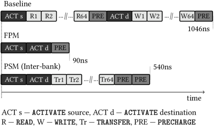
Table 5.3 shows the reduction in latency and energy consumption due to our mechanisms for different cases of 4KB copy and zeroing operations. To be fair to the baseline, the results include only the energy consumed by the DRAM and the DRAM channel. We draw two conclusions from our results.
| Mechanism | Absolute | Reduction | |||
|---|---|---|---|---|---|
| Memory | Memory | ||||
| Latency | Energy | Latency | Energy | ||
| (ns) | (J) | ||||
| Copy | Baseline | 1046 | 3.6 | 1.00x | 1.0x |
| FPM | 90 | 0.04 | 11.62x | 74.4x | |
| Inter-Bank - PSM | 540 | 1.1 | 1.93x | 3.2x | |
| Intra-Bank - PSM | 1050 | 2.5 | 0.99x | 1.5x | |
| Zero | Baseline | 546 | 2.0 | 1.00x | 1.0x |
| FPM | 90 | 0.05 | 6.06x | 41.5x | |
First, FPM significantly improves both the latency and the energy consumed by bulk operations — 11.6x and 6x reduction in latency of 4KB copy and zeroing, and 74.4x and 41.5x reduction in memory energy of 4KB copy and zeroing. Second, although PSM does not provide as much benefit as FPM, it still reduces the latency and energy of a 4KB inter-bank copy by 1.9x and 3.2x, while providing a more generally applicable mechanism.
When an on-chip cache is employed, any line cached from the source or destination page can be served at a lower latency than accessing main memory. As a result, in such systems, the baseline will incur a lower latency to perform a bulk copy or initialization compared to a system without on-chip caches. However, as we show in the following sections (5.5.2–5.5.4), even in the presence of on-chip caching, the raw latency/energy improvement due to RowClone translates to significant improvements in both overall system performance and energy efficiency.
5.5.2 The fork System Call
As mentioned in Section 5.3.2, fork is one of the most expensive yet frequently-used system calls in modern systems [186]. Since fork triggers a large number of CoW operations (as a result of updates to shared pages from the parent or child process), RowClone can significantly improve the performance of fork.
The performance of fork depends on two parameters: 1) the size of the address space used by the parent—which determines how much data may potentially have to be copied, and 2) the number of pages updated after the fork operation by either the parent or the child—which determines how much data is actually copied. To exercise these two parameters, we create a microbenchmark, forkbench, which first creates an array of size and initializes the array with random values. It then forks itself. The child process updates random pages (by updating a cache line within each page) and exits; the parent process waits for the child process to complete before exiting itself.
As such, we expect the number of copy operations to depend on —the number of pages copied. Therefore, one may expect RowClone’s performance benefits to be proportional to . However, an application’s performance typically depends on the overall memory access rate [215], and RowClone can only improve performance by reducing the memory access rate due to copy operations. As a result, we expect the performance improvement due to RowClone to primarily depend on the fraction of memory traffic (total bytes transferred over the memory channel) generated by copy operations. We refer to this fraction as FMTC—Fraction of Memory Traffic due to Copies.
Figure 5.4 plots FMTC of forkbench for different values of (64MB and 128MB) and (2 to 16k) in the baseline system. As the figure shows, for both values of , FMTC increases with increasing . This is expected as a higher (more pages updated by the child) leads to more CoW operations. However, because of the presence of other read/write operations (e.g., during the initialization phase of the parent), for a given value of , FMTC is larger for = 64MB compared to = 128MB. Depending on the value of and , anywhere between 14% to 66% of the memory traffic arises from copy operations. This shows that accelerating copy operations using RowClone has the potential to significantly improve the performance of the fork operation.
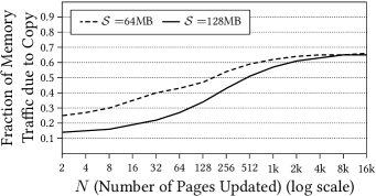
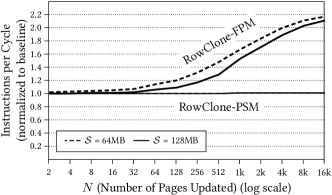
Figure 5.5 plots the performance (IPC) of FPM and PSM for forkbench, normalized to that of the baseline system. We draw two conclusions from the figure. First, FPM improves the performance of forkbench for both values of and most values of . The peak performance improvement is 2.2x for = 16k (30% on average across all data points). As expected, the improvement of FPM increases as the number of pages updated increases. The trend in performance improvement of FPM is similar to that of FMTC (Figure 5.4), confirming our hypothesis that FPM’s performance improvement primarily depends on FMTC. Second, PSM does not provide considerable performance improvement over the baseline. This is because the large on-chip cache in the baseline system buffers the writebacks generated by the copy operations. These writebacks are flushed to memory at a later point without further delaying the copy operation. As a result, PSM, which just overlaps the read and write operations involved in the copy, does not improve latency significantly in the presence of a large on-chip cache. On the other hand, FPM, by copying all cache lines from the source row to destination in parallel, significantly reduces the latency compared to the baseline (which still needs to read the source blocks from main memory), resulting in high performance improvement.
Figure 5.6 shows the reduction in DRAM energy consumption (considering both the DRAM and the memory channel) of FPM and PSM modes of RowClone compared to that of the baseline for forkbench with MB. Similar to performance, the overall DRAM energy consumption also depends on the total memory access rate. As a result, RowClone’s potential to reduce DRAM energy depends on the fraction of memory traffic generated by copy operations. In fact, our results also show that the DRAM energy reduction due to FPM and PSM correlate well with FMTC (Figure 5.4). By efficiently performing the copy operations, FPM reduces DRAM energy consumption by up to 80% (average 50%, across all data points). Similar to FPM, the energy reduction of PSM also increases with increasing with a maximum reduction of 9% for =16k.
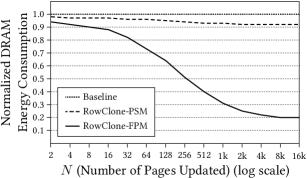
In a system that is agnostic to RowClone, we expect the performance improvement and energy reduction of RowClone to be in between that of FPM and PSM. By making the system software aware of RowClone (Section 5.2.3), we can approximate the maximum performance and energy benefits by increasing the likelihood of the use of FPM.
5.5.3 Copy/Initialization Intensive Applications
In this section, we analyze the benefits of RowClone on six copy/initialization intensive applications, including one instance of the forkbench described in the previous section. Table 5.4 describes these applications.
| Name | Description |
|---|---|
| bootup | A phase booting up the Debian operating system. |
| compile | The compilation phase from the GNU C compiler (while running cc1). |
| forkbench | An instance of the forkbench described in Section 5.5.2 with = 64MB and = 1k. |
| mcached | Memcached [8], a memory object caching system, a phase inserting many key-value pairs into the memcache. |
| mysql | MySQL [9], an on-disk database system, a phase loading the sample employeedb |
| shell | A Unix shell script running ‘find’ on a directory tree with ‘ls’ on each sub-directory (involves filesystem accesses and spawning new processes). |
Figure 5.7 plots the fraction of memory traffic due to copy, initialization, and regular read/write operations for the six applications. For these applications, between 10% and 80% of the memory traffic is generated by copy and initialization operations.
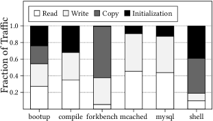
Figure 5.8 compares the IPC of the baseline with that of RowClone and a variant of RowClone, RowClone-ZI (described shortly). The RowClone-based initialization mechanism slightly degrades performance for the applications which have a negligible number of copy operations (mcached, compile, and mysql).
Further analysis indicated that, for these applications, although the operating system zeroes out any newly allocated page, the application typically accesses almost all cache lines of a page immediately after the page is zeroed out. There are two phases: 1) the phase when the OS zeroes out the page, and 2) the phase when the application accesses the cache lines of the page. While the baseline incurs cache misses during phase 1, RowClone, as a result of performing the zeroing operation completely in memory, incurs cache misses in phase 2. However, the baseline zeroing operation is heavily optimized for memory-level parallelism (MLP) [155, 158]. In contrast, the cache misses in phase 2 have low MLP. As a result, incurring the same misses in Phase 2 (as with RowClone) causes higher overall stall time for the application (because the latencies for the misses are serialized) than incurring them in Phase 1 (as in the baseline), resulting in RowClone’s performance degradation compared to the baseline.
To address this problem, we introduce a variant of RowClone, RowClone-Zero-Insert (RowClone-ZI). RowClone-ZI not only zeroes out a page in DRAM but it also inserts a zero cache line into the processor cache corresponding to each cache line in the page that is zeroed out. By doing so, RowClone-ZI avoids the cache misses during both phase 1 (zeroing operation) and phase 2 (when the application accesses the cache lines of the zeroed page). As a result, it improves performance for all benchmarks, notably forkbench (by 66%) and shell (by 40%), compared to the baseline.
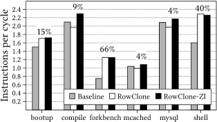
Table 5.5 shows the percentage reduction in DRAM energy and memory bandwidth consumption with RowClone and RowClone-ZI compared to the baseline. While RowClone significantly reduces both energy and memory bandwidth consumption for bootup, forkbench and shell, it has negligible impact on both metrics for the remaining three benchmarks. The lack of energy and bandwidth benefits in these three applications is due to serial execution caused by the the cache misses incurred when the processor accesses the zeroed out pages (i.e., phase 2, as described above), which also leads to performance degradation in these workloads (as also described above). RowClone-ZI, which eliminates the cache misses in phase 2, significantly reduces energy consumption (between 15% to 69%) and memory bandwidth consumption (between 16% and 81%) for all benchmarks compared to the baseline. We conclude that RowClone-ZI can effectively improve performance, memory energy, and memory bandwidth efficiency in page copy and initialization intensive single-core workloads.
| Application | Energy Reduction | Bandwidth Reduction | ||
|---|---|---|---|---|
| RowClone | +ZI | RowClone | +ZI | |
| bootup | 39% | 40% | 49% | 52% |
| compile | -2% | 32% | 2% | 47% |
| forkbench | 69% | 69% | 60% | 60% |
| mcached | 0% | 15% | 0% | 16% |
| mysql | -1% | 17% | 0% | 21% |
| shell | 68% | 67% | 81% | 81% |
5.5.4 Multi-core Evaluations
As RowClone performs bulk data operations completely within DRAM, it significantly reduces the memory bandwidth consumed by these operations. As a result, RowClone can benefit other applications running concurrently on the same system. We evaluate this benefit of RowClone by running our copy/initialization-intensive applications alongside memory-intensive applications from the SPEC CPU2006 benchmark suite [55] (i.e., those applications with last-level cache MPKI greater than 1). Table 5.6 lists the set of applications used for our multi-programmed workloads.
| Copy/Initialization-intensive benchmarks |
| bootup, compile, forkbench, mcached, mysql, shell |
| Memory-intensive benchmarks from SPEC CPU2006 |
| bzip2, gcc, mcf, milc, zeusmp, gromacs, cactusADM, leslie3d, namd, gobmk, dealII, soplex, hmmer, sjeng, GemsFDTD, libquantum, h264ref, lbm, omnetpp, astar, wrf, sphinx3, xalancbmk |
We generate multi-programmed workloads for 2-core, 4-core and 8-core systems. In each workload, half of the cores run copy/initialization-intensive benchmarks and the remaining cores run memory-intensive SPEC benchmarks. Benchmarks from each category are chosen at random.
Figure 5.9 plots the performance improvement due to RowClone and RowClone-ZI for the 50 4-core workloads we evaluated (sorted based on the performance improvement due to RowClone-ZI). Two conclusions are in order. First, although RowClone degrades performance of certain 4-core workloads (with compile, mcached or mysql benchmarks), it significantly improves performance for all other workloads (by 10% across all workloads). Second, like in our single-core evaluations (Section 5.5.3), RowClone-ZI eliminates the performance degradation due to RowClone and consistently outperforms both the baseline and RowClone for all workloads (20% on average).
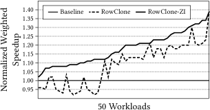
Table 5.7 shows the number of workloads and six metrics that evaluate the performance, fairness, memory bandwidth and energy efficiency improvement due to RowClone compared to the baseline for systems with 2, 4, and 8 cores. For all three systems, RowClone significantly outperforms the baseline on all metrics.
| Number of Cores | 2 | 4 | 8 |
|---|---|---|---|
| Number of Workloads | 138 | 50 | 40 |
| Weighted Speedup [67] Improvement | 15% | 20% | 27% |
| Instruction Throughput Improvement | 14% | 15% | 25% |
| Harmonic Speedup [147] Improvement | 13% | 16% | 29% |
| Maximum Slowdown [123, 124] Reduction | 6% | 12% | 23% |
| Memory Bandwidth/Instruction [205] Reduction | 29% | 27% | 28% |
| Memory Energy/Instruction Reduction | 19% | 17% | 17% |
To provide more insight into the benefits of RowClone on multi-core systems, we classify our copy/initialization-intensive benchmarks into two categories: 1) Moderately copy/initialization-intensive (compile, mcached, and mysql) and highly copy/initialization-intensive (bootup, forkbench, and shell). Figure 5.10 shows the average improvement in weighted speedup for the different multi-core workloads, categorized based on the number of highly copy/initialization-intensive benchmarks. As the trends indicate, the performance improvement increases with increasing number of such benchmarks for all three multi-core systems, indicating the effectiveness of RowClone in accelerating bulk copy/initialization operations.
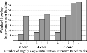
We conclude that RowClone is an effective mechanism to improve system performance, energy efficiency and bandwidth efficiency of future, bandwidth-constrained multi-core systems.
5.5.5 Memory-Controller-based DMA
One alternative way to perform a bulk data operation is to use the memory controller to complete the operation using the regular DRAM interface (similar to some prior approaches [113, 248]). We refer to this approach as the memory-controller-based DMA (MC-DMA). MC-DMA can potentially avoid the cache pollution caused by inserting blocks (involved in the copy/initialization) unnecessarily into the caches. However, it still requires data to be transferred over the memory bus. Hence, it suffers from the large latency, bandwidth, and energy consumption associated with the data transfer. Because the applications used in our evaluations do not suffer from cache pollution, we expect the MC-DMA to perform comparably or worse than the baseline. In fact, our evaluations show that MC-DMA degrades performance compared to our baseline by 2% on average for the six copy/initialization intensive applications (16% compared to RowClone). In addition, the MC-DMA does not conserve any DRAM energy, unlike RowClone.
5.6 Summary
In this chapter, we introduced RowClone, a technique for exporting bulk data copy and initialization operations to DRAM. Our fastest mechanism copies an entire row of data between rows that share a row buffer, with very few changes to the DRAM architecture, while leading to significant reduction in the latency and energy of performing bulk copy/initialization. We also propose a more flexible mechanism that uses the internal bus of a chip to copy data between different banks within a chip. Our evaluations using copy and initialization intensive applications show that RowClone can significantly reduce memory bandwidth consumption for both single-core and multi-core systems (by 28% on average for 8-core systems), resulting in significant system performance improvement and memory energy reduction (27% and 17%, on average, for 8-core systems).
We conclude that our approach of performing bulk copy and initialization completely in DRAM is effective in improving both system performance and energy efficiency for future, bandwidth-constrained, multi-core systems. We hope that greatly reducing the bandwidth, energy and performance cost of bulk data copy and initialization can lead to new and easier ways of writing applications that would otherwise need to be designed to avoid bulk data copy and initialization operations.
Chapter 6 Buddy RAM
A part of this chapter is originally published as “Fast Bulk Bitwise AND and OR in DRAM” in IEEE Computer Architecture Letters, 2015 [191]
In the line of research aiming to identify primitives that can be efficiently performed inside DRAM, the second mechanism we explore in this thesis is one that can perform bitwise logical operations completely inside DRAM. Our mechanism uses the internal analog operation of DRAM to efficiently perform bitwise operations. For this reason, we call our mechanism Buddy RAM or Bitwise-ops Using DRAM (BU-D-RAM).
Bitwise operations are an important component of modern day programming. They have a wide variety of applications, and can often replace arithmetic operations with more efficient algorithms [126, 232]. In fact, many modern processors provide support for accelerating a variety of bitwise operations (e.g., Intel Advance Vector eXtensions [98]).
We focus our attention on bitwise operations on large amounts of input data. We refer to such operations as bulk bitwise operations. Many applications trigger such bulk bitwise operations. For example, in databases, bitmap indices [41, 164] can be more efficient than commonly-used B-trees for performing range queries and joins [41, 5, 238]. In fact, bitmap indices are supported by many real-world implementations (e.g., Redis [10], Fastbit [5]). Improving the throughput of bitwise operations can boost the performance of such bitmap indices and many other primitives (e.g., string matching, bulk hashing).
As bitwise operations are computationally inexpensive, in existing systems, the throughput of bulk bitwise operations is limited by the available memory bandwidth. This is because, to perform a bulk bitwise operation, existing systems must first read the source data from main memory into the processor caches. After performing the operation at the processor, they may have to write the result back to main memory. As a result, this approach requires a large amount of data to be transferred back and forth on the memory channel, resulting in high latency, bandwidth, and energy consumption.
Our mechanism, Buddy RAM, consist of two components: one to perform bitwise AND/OR operations (Buddy-AND/OR), and the second component to perform bitwise NOT operations (Buddy-NOT). Both components heavily exploit the operation of the sense amplifier and the DRAM cells (described in Section 4.2.2). In the following sections, we first provide an overview of both these mechanisms, followed by a detailed implementation of Buddy that requires minimal changes to the internal design and the external interface of commodity DRAM.
6.1 Buddy-AND/OR
As described in Section 4.2.2, when a DRAM cell is connected to a bitline precharged to VDD, the cell induces a deviation on the bitline, and the deviation is amplified by the sense amplifier. Buddy-AND/OR exploits the following fact about the cell operation.
The final state of the bitline after amplification is determined solely by the deviation on the bitline after the charge sharing phase (after state ➌ in Figure 4.6). If the deviation is positive (i.e., towards VDD), the bitline is amplified to VDD. Otherwise, if the deviation is negative (i.e., towards ), the bitline is amplified to .
6.1.1 Triple-Row Activation
Buddy-AND/OR simultaneously connects three cells to a sense amplifier. When three cells are connected to the bitline, the deviation of the bitline after charge sharing is determined by the majority value of the three cells. Specifically, if at least two cells are initially in the charged state, the effective voltage level of the three cells is at least VDD. This results in a positive deviation on the bitline. On the other hand, if at most one cell is initially in the charged state, the effective voltage level of the three cells is at most VDD. This results in a negative deviation on the bitline voltage. As a result, the final state of the bitline is determined by the logical majority value of the three cells.
Figure 6.1 shows an example of activating three cells simultaneously. In the figure, we assume that two of the three cells are initially in the charged state and the third cell is in the empty state ➊. When the wordlines of all the three cells are raised simultaneously ➋, charge sharing results in a positive deviation on the bitline.
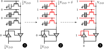
More generally, if the cell’s capacitance is , the the bitline’s is , and if of the three cells are initially in the charged state, based on the charge sharing principles [118], the deviation on the bitline voltage level is given by,
| (6.1) | |||||
From the above equation, it is clear that is positive for , and is negative for . Therefore, after amplification, the final voltage level on the bitline is VDD for and for .
If , , and represent the logical values of the three cells, then the final state of the bitline is (i.e., at least two of the values should be for the final state to be ). Importantly, using simple boolean algebra, this expression can be rewritten as . In other words, if the initial state of is , then the final state of the bitline is a bitwise OR of and . Otherwise, if the initial state of is , then the final state of the bitline is a bitwise AND of and . Therefore, by controlling the value of the cell C, we can execute a bitwise AND or bitwise OR operation of the remaining two cells using the sense amplifier. Due to the regular bulk operation of cells in DRAM, this approach naturally extends to an entire row of DRAM cells and sense amplifiers, enabling a multi-kilobyte-wide bitwise AND/OR operation.111Note that the triple-row activation by itself can be useful to implement a bitwise majority primitive. However, we do not explore this path in this thesis.
6.1.2 Challenges
There are two challenges in our approach. First, Equation 6.1 assumes that the cells involved in the triple-row activation are either fully charged or fully empty. However, DRAM cells leak charge over time. Therefore, the triple-row activation may not operate as expected. This problem may be exacerbated by process variation in DRAM cells. Second, as shown in Figure 6.1 (state ➌), at the end of the triple-row activation, the data in all the three cells are overwritten with the final state of the bitline. In other words, our approach overwrites the source data with the final value. In the following sections, we propose a simple implementation that addresses these challenges.
6.1.3 Overview of Implementation of Buddy-AND/OR
To ensure that the source data does not get modified, our mechanism first copies the data from the two source rows to two reserved temporary rows ( and ). Depending on the operation to be performed (AND or OR), our mechanism initializes a third reserved temporary row to ( or ). It then simultaneously activates the three rows , , and . It finally copies the result to the destination row. For example, to perform a bitwise AND of two rows and and store the result in row , our mechanism performs the following steps.
-
1.
Copy data of row to row
-
2.
Copy data of row to row
-
3.
Initialize row to
-
4.
Activate rows , , and simultaneously
-
5.
Copy data of row to row
While the above mechanism is simple, the copy operations, if performed naively, will nullify the benefits of our mechanism. Fortunately, we can use RowClone (described in Chapter 5), to perform row-to-row copy operations quickly and efficiently within DRAM. To recap, RowClone consists of two techniques. The first technique, RowClone-FPM (Fast Parallel Mode), which is the fastest and the most efficient, copies data within a subarray by issuing two back-to-back ACTIVATEs to the source row and the destination row, without an intervening PRECHARGE. The second technique, RowClone-PSM (Pipelined Serial Mode), efficiently copies data between two banks by using the shared internal bus to overlap the read to the source bank with the write to the destination bank.
With RowClone, all three copy operations (Steps 1, 2, and 5) and the initialization operation (Step 3) can be performed efficiently within DRAM. To use RowClone for the initialization operation, we reserve two additional rows, and . is pre-initialized to and is pre-initialized to 1. Depending on the operation to be performed, our mechanism uses RowClone to copy either or to . Furthermore, to maximize the use of RowClone-FPM, we reserve five rows in each subarray to serve as the temporary rows (, , and ) and the control rows ( and ).
In the best case, when all the three rows involved in the operation (, , and ) are in the same subarray, our mechanism can use RowClone-FPM for all copy and initialization operations. However, if the three rows are in different banks/subarrays, some of the three copy operations have to use RowClone-PSM. In the worst case, when all three copy operations have to use RowClone-PSM, our approach will consume higher latency than the baseline. However, when only one or two RowClone-PSM operations are required, our mechanism will be faster and more energy-efficient than existing systems. As our goal in this paper is to demonstrate the power of our approach, in the rest of the paper, we will focus our attention on the case when all rows involved in the bitwise operation are in the same subarray.
6.1.4 Reliability of Our Mechanism
While our mechanism trivially addresses the second challenge (modification of the source data), it also addresses the first challenge (DRAM cell leakage). This is because, in our approach, the source (and the control) data are copied to the rows , and just before the triple-row activation. Each copy operation takes much less than , which is five orders of magnitude less than the typical refresh interval (). Consequently, the cells involved in the triple-row activation are very close to the fully refreshed state before the operation, thereby ensuring reliable operation of the triple-row activation. Having said that, an important aspect of our mechanism is that a chip that fails the tests for triple-row activation (e.g., due to process variation) can still be used as a regular DRAM chip. As a result, our approach is likely to have little impact on the overall yield of DRAM chips, which is a major concern for manufacturers.
6.2 Buddy-NOT
Buddy-NOT exploits the fact that the sense amplifier itself consists of two inverters and the following observation about the sense amplifier operation.
At the end of the sense amplification process, while the bitline voltage reflects the logical value of the cell, the voltage level of the corresponds to the negation of the logical value of the cell.
6.2.1 Dual-Contact Cell
Our high-level idea is to transfer the data on the to a cell that can be connected to the bitline. For this purpose, we introduce a special DRAM cell called dual-contact cell. A dual-contact cell (DCC) is a DRAM cell with two transistors and one capacitor. For each DCC, one transistor connects the DCC to the bitline and the other transistor connects the DCC to the . Each of the two transistors is controlled by a different wordline. We refer to the wordline that controls the connection between the DCC and the bitline as the d-wordline (or data wordline). We refer to the wordline that controls the connection between the DCC and the as the n-wordline (or negation wordline). Figure 6.2 shows one DCC connected to a sense amplifier. In our mechanism, we use two DCCs for each sense amplifier, one on each side of the sense amplifier.
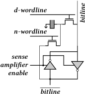
6.2.2 Exploiting the Dual-Contact Cell
Since the DCC is connected to both the bitline and the , we can use a RowClone-like mechanism to transfer the negation of some source data on to the DCC using the n-wordline. The negated data can be transferred to the bitline by activating the d-wordline of the DCC, and can then be copied to the destination cells using RowClone.
Figure 6.3 shows the sequence of steps involved in transferring the negation of a source cell on to the DCC. The figure shows a source cell and a DCC connected to the same sense amplifier ➊. Our mechanism first activates the source cell ➋. At the end of the activation process, the bitline is driven to the data corresponding to the source cell, VDD in this case ➌. More importantly, for the purpose of our mechanism, the is driven to . In this state, our mechanism activates the n-wordline, enabling the transistor that connects the DCC to the ➍. Since the is already at a stable voltage level of , it overwrites the value in the cell with , essentially copying the negation of the source data into the DCC. After this step, the negated data can be efficiently copied into the destination cell using RowClone. Section 6.3.3 describes the sequence of commands required to perform a bitwise NOT.
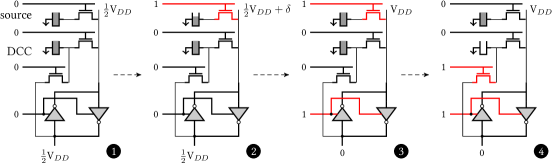
6.3 Implementation and Hardware Cost
Besides the addition of a dual-contact cell on either side of each sense amplifier, Buddy primarily relies on different variants and sequences of row activations to perform bulk bitwise operations. As a result, the main changes to the DRAM chip introduced by Buddy are to the row decoding logic. While the operation of Buddy-NOT is similar to a regular cell operation, Buddy-AND/OR requires three rows to be activated simultaneously. Activating three arbitrary rows within a subarray 1) requires the memory controller to first communicate the three addresses to DRAM, and 2) requires DRAM to simultaneously decode the three addresses. Both of these requirements incur huge cost, i.e., wide address buses and three full row decoders to decode the three addresses simultaneously.
In this work, we propose an implementation with much lower cost. At a high level, we reserve a small fraction of row addresses within each subarray for triple-row activation. Our mechanism maps each reserved address to a pre-defined set of three wordlines instead of one. With this approach, the memory controller can perform a triple-row activation by issuing an ACTIVATE with a single row address. We now describe how we exploit certain properties of Buddy to realize this implementation.
6.3.1 Row Address Grouping
Before performing the triple-row activation, our mechanism copies the source data and the control data to three temporary rows (Section 6.1.3). If we choose these temporary rows at design time, then these rows can be controlled using a separate small row decoder. To exploit this idea, we divide the space of row addresses within each subarray into three distinct groups (B, C, and D), as shown in Figure 6.4.
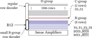
The B-group (or the bitwise group) corresponds to rows that are used to perform the bitwise operations. This group contains addresses that map to physical wordlines. Four of the eight wordlines are the d-and-n-wordlines that control the two rows of dual-contact cells. We will refer to the d-wordlines of the two rows as DCC0 and DCC1, and the corresponding n-wordlines as and . The remaining four wordlines control four temporary rows of DRAM cells that will be used by various bitwise operations. We refer to these rows as T0—T3. While some B-group addresses activate individual wordlines, others activate multiple wordlines simultaneously. Table 6.1 lists the mapping between the 16 addresses and the wordlines. Addresses B0—B7 individually activate one of the physical wordlines. Addresses B12—B15 activate three wordlines simultaneously. These addresses will be used by the memory controller to trigger bitwise AND or OR operations. Finally, addresses B8—B11 activate two wordlines. As we will show in the next section, these addresses will be used to copy the result of an operation simultaneously to two rows (e.g., zero out two rows simultaneously).
| Addr. | Wordline(s) |
|---|---|
| B0 | T0 |
| B1 | T1 |
| B2 | T2 |
| B3 | T3 |
| B4 | DCC0 |
| B5 | |
| B6 | DCC1 |
| B7 |
| Addr. | Wordline(s) |
|---|---|
| B8 | , T0 |
| B9 | , T1 |
| B10 | T2, T3 |
| B11 | T0, T3 |
| B12 | T0, T1, T2 |
| B13 | T1, T2, T3 |
| B14 | DCC0, T1, T2 |
| B15 | DCC1, T0, T3 |
The C-group (or the control group) contains the rows that store the pre-initialized values for controlling the bitwise AND/OR operations. Specifically, this group contains only two addresses: C0 and C1. The rows corresponding to C0 and C1 are initialized to all-zeros and all-ones, respectively.
The D-group (or the data group) corresponds to the rows that store regular user data. This group contains all the addresses in the space of row addresses that are neither in the B-group nor in the C-group. Specifically, if each subarray contains rows, then the D-group contains addresses, labeled D0—D1005.
With these different address groups, the memory controller can simply use the existing command interface and use the ACTIVATE commands to communicate all variants of the command to the DRAM chips. Depending on the address group, the DRAM chips can internally process the activate command appropriately, e.g., perform a triple-row activation. For instance, by just issuing an ACTIVATE to address B12, the memory controller can simultaneously activate rows T0, T1, and T2, as illustrated in Figure 6.4.
6.3.2 Split Row Decoder
Our idea of split row decoder splits the row decoder into two parts. The first part controls addresses from only the B-group, and the second part controls addresses from the C-group and the D-group (as shown in Figure 6.4). There are two benefits to this approach. First, the complexity of activating multiple wordlines is restricted to the small decoder that controls only the B-group. In fact, this decoder takes only a 4-bit input (16 addresses) and generates a 8-bit output (8 wordlines). In contrast, as described in the beginning of this section, a naive mechanism to simultaneously activate three arbitrary rows incurs high cost. Second, as we will describe in Section 6.3.3, the memory controller must perform several back-to-back ACTIVATEs to execute various bitwise operations. In a majority of cases, the two rows involved in each back-to-back ACTIVATEs are controlled by different decoders. This enables an opportunity to overlap the two ACTIVATEs, thereby significantly reducing their latency. We describe this optimization in detail in Section 6.3.4. Although the groups of addresses and the corresponding row decoders are logically split, the physical implementation can use a single large decoder with the wordlines from different groups interleaved, if necessary.
6.3.3 Executing Bitwise Ops: The AAP Primitive
To execute each bitwise operations, the memory controller must send a sequence of commands. For example, to perform the bitwise NOT operation, Dk = not Di, the memory controller sends the following sequence of commands.
-
1.
ACTIVATE Di
-
2.
ACTIVATE B5
-
3.
PRECHARGE
-
4.
ACTIVATE B4
-
5.
ACTIVATE Dk
-
6.
PRECHARGE
Step 1 transfers the data from the source row to the array of sense amplifiers. Step 2 activates the n-wordline of one of the DCCs, which connects the dual-contact cells to the corresponding s. As a result, this step stores the negation of the source cells into the corresponding DCC row (as described in Figure 6.3). After the precharge operation in Step 3, Step 4 activates the d-wordline of the DCC row, transferring the negation of the source data on to the bitlines. Finally, Step 5 activates the destination row. Since the sense amplifiers are already activated, this step copies the data on the bitlines, i.e., the negation of the source data, to the destination row. Step 6 completes the negation operation by precharging the bank.
If we observe the negation operation, it consists of two steps of
ACTIVATE-ACTIVATE-PRECHARGE operations. We refer to this sequence of
operations as the A&Aprimitive. Each A&Atakes two addresses as
input. A&A(row1, row2) corresponds to the following
sequence of commands:
ACTIVATE row1; ACTIVATE row2; PRECHARGE;
With the A&Aprimitive, the not operation, Dk = not Di, can be rewritten as,
-
1.
A&A(Di, B5) ; DCC = not Di
-
2.
A&A(B4, Dk) ; Dk = DCC
In fact, we observe that all the bitwise operations mainly involve a sequence of A&Aoperations. Sometimes, they require a regular ACTIVATE followed by a PRECHARGE operation. We will use AP to refer to such operations. Figure 6.5 shows the sequence of steps taken by the memory controller to execute seven bitwise operations: not, and, or, nand, nor, xor, and xnor. Each step is annotated with the logical result of performing the step.
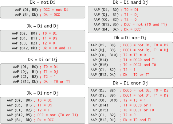
As an illustration, let us consider the and operation, Dk = Di and Dj. The first step (A&A(Di, B0)) first activates the source row Di, followed by the temporary row T0 (which corresponds to address B0). As a result, this operation copies the data of Di to the temporary row T0. Similarly, the second step (A&A(Dj, B1)) copies the data of the source row Dj to the temporary row T1, and the third step A&A(C0, B2) copies the data of the control row “0” to the temporary row T2. Finally, the last step (A&A(B12, Dk)) first issues an ACTIVATE to address B12. As described in Table 6.1 and illustrated in Figure 6.4, this command simultaneously activates the rows T0, T1, and T2, resulting in a and operation of the values of rows T0 and T1. As this command is immediately followed by an ACTIVATE to Dk, the result of the and operation is copied to the destination row Dk.
6.3.4 Accelerating the AAP Primitive
It is clear from Figure 6.5 that the latency of executing any bitwise operation using Buddy depends on the latency of executing the A&Aprimitive. The latency of the A&Aprimitive in turn depends on the latency of the ACTIVATE and the PRECHARGE operations. In the following discussion, we assume DDR3-1600 (8-8-8) timing parameters [108]. For these parameters, the latency of an ACTIVATE operation is t = 35 ns, and the latency of a PRECHARGE operation is t = 10 ns.
Naive Execution of AAP.
The naive approach is to perform the three operations involved in A&Aserially one after the other. Using this simple approach, the latency of the A&Aoperation is 2t + t = 80 ns. While Buddy outperforms existing systems even with this naive approach, we exploit some properties of A&Ato further reduce its latency.
Shortening the Second ACTIVATE.
We observe that the second ACTIVATE operation is issued when the bank is already activated. As a result, this ACTIVATE does not require the full sense-amplification process, which is the dominant source of the latency of an ACTIVATE. In fact, the second ACTIVATE of an A&Aonly requires the corresponding wordline to be raised, and the bitline data to overwrite the cell data. We introduce a new timing parameter called t, to capture the latency of these steps. With this optimization, the latency of A&Ais t + t + t.
Overlapping the Two ACTIVATEs.
For all the bitwise operations (Figure 6.5), with the exception of one A&Aeach in nand and nor, exactly one of the two ACTIVATEs in each A&Ais to a B-group address. Since the wordlines in B-group are controlled by a different row decoder (Section 6.3.2), we can overlap the two ACTIVATEs of the A&Aprimitive. More precisely, if the second ACTIVATE is issued after the first activation has sufficiently progressed, the sense amplifiers will force the data of the second row to the result of the first activation. This operation is similar to the inter-segment copy operation in Tiered-Latency DRAM [137] (Section 4.4). Based on SPICE simulations, the latency of the executing both the ACTIVATEs is 4 ns larger than t. Therefore, with this optimization, the latency of A&Ais t + 4 ns + t = 49 ns.
6.3.5 DRAM Chip and Controller Cost
Buddy has three main sources of cost to the DRAM chip. First, Buddy requires changes to the row decoding logic. Specifically, the row decoding logic must distinguish between the B-group addresses and the remaining addresses. Within the B-group, it must implement the mapping between the addresses and the wordlines described in Table 6.1. As described in Section 6.3.1, the B-group contains only 16 addresses that are mapped to 8 wordlines. As a result, we expect the complexity of the changes to the row decoding logic to be low.
The second source of cost is the design and implementation of the dual-contact cells (DCCs). In our design, each sense amplifier has only one DCC on each side, and each DCC has two wordlines associated with it. Consequently, there is enough space to implement the second transistor that connects the DCC to the corresponding . In terms of area, the cost of each DCC is roughly equivalent to two regular DRAM cells. As a result, we can view each row of DCCs as two rows of regular DRAM cells.
The third source of cost is the capacity lost as a result of reserving the rows in the B-group and C-group. The rows in these groups are reserved for the memory controller to perform bitwise operations and cannot be used to store application data (Section 6.3.1). Our proposed implementation of Buddy reserves 18 addresses in each subarray for the two groups. For a typical subarray size of 1024 rows, the loss in memory capacity is 1%.
On the controller side, Buddy requires the memory controller to 1) store information about different address groups, 2) track the timing for different variants of the ACTIVATE (with or without the optimizations), and 3) track the status of different on-going bitwise operations. While scheduling different requests, the controller 1) adheres to power constraints like tFAW which limit the number of full row activations during a given time window, and 2) can interleave the multiple AAP commands to perform a bitwise operation with other requests from different applications. We believe this modest increase in the DRAM chip/controller complexity and capacity cost is negligible compared to the improvement in throughput and performance enabled by Buddy.
6.4 End-to-end System Support
We envision two distinct ways of integrating Buddy with the rest of the system. The first way is a loose integration, where Buddy is treated as an accelerator (similar to a GPU). The second way is a much tighter integration, where Buddy is supported by the main memory. In this section, we discuss these two ways along with their pros and cons.
6.4.1 Buddy as an Accelerator
Treating Buddy as an accelerator is probably the simplest way of integrating Buddy into a system. In this approach, the manufacturer of Buddy RAM designs the accelerator that can be plugged into the system as a separate device (e.g., PCIe). While this mechanism requires communication between the CPU and the Buddy accelerator, there are benefits to this approach that lower the cost of integration. First, a single manufacturer can design both the DRAM and the memory controller (which is not true about commodity DRAM). Second, the details of the data mapping to suit Buddy can be hidden behind the device driver, which can expose a simple-to-use API to the applications.
6.4.2 Integrating Buddy with System Main Memory
A tighter integration of Buddy with the system main memory requires support from different layers of the system stack, which we discuss below.
ISA Support
For the processor to exploit Buddy, it must be able to identify
and export instances of bulk bitwise operations to the memory
controller. To enable this, we introduce new instructions that
will allow software to directly communicate instances of bulk
bitwise operations to the processor. Each new instruction takes
the following form:
bop dst, src1, [src2], size
where bop is the bitwise operation to be performed, dst is the address of the destination, src1 and src2 correspond to the addresses of the source, and size denotes the length of the vectors on which the bitwise operations have to be performed. The microarchitectural implementation of these instructions will determine whether each instance of these instructions can be accelerated using Buddy.
Implementing the New Buddy Instructions.
The microarchitectural implementation of the new instructions will determine whether each instance can be accelerated using Buddy. Buddy imposes two constraints on the data it operates on. First, both the source data and the destination data should be within the same subarray. Second, all Buddy operations are performed on an entire row of data. As a result, the source and destination data should be row-aligned and the operation should span at least an entire row. The microarchitecture ensures that these constraints are satisfied before performing the Buddy operations. Specifically, if the source and destination rows are not in the same subarray, the processor can either 1) use RowClone-PSM [192] to copy the data into the same subarray, or 2) execute the operation using the CPU. This choice can be dynamically made depending on the number of RowClone-PSM operations required and the memory bandwidth contention. If the processor cannot ensure data alignment, or if the size of the operation is smaller than the DRAM row size, it can execute the operations using the CPU. However, with careful application design and operating system support, the system can maximize the use of Buddy to extract its performance and efficiency benefits.
Maintaining On-chip Cache Coherence.
Buddy directly reads/modifies data in main memory. As a result, we need a mechanism to ensure the coherence of data present in the on-chip caches. Specifically, before performing any Buddy operation, the memory controller must first flush any dirty cache lines from the source rows and invalidate any cache lines from destination rows. While flushing the dirty cache lines of the source rows is on the critical path of any Buddy operation, we can speed up using the Dirty-Block Index (described in Chapter 8). In contrast, the cache lines of the destination rows can be invalidated in parallel with the Buddy operation. The mechanism required to maintain cache coherence introduces a small performance overhead. However, for applications with large amounts of data, since the cache contains only a small fraction of the data, the performance benefits of our mechanism significantly outweigh the overhead of maintaining coherence, resulting in a net gain in both performance and efficiency.
Software Support
The minimum support that Buddy requires from software is for the application to use the new Buddy instructions to communicate the occurrences of bulk bitwise operations to the processor. However, with careful memory allocation support from the operating system, the application can maximize the benefits it can extract from Buddy. Specifically, the OS must allocate pages that are likely to be involved in a bitwise operation such that 1) they are row-aligned, and 2) belong to the same subarray. Note that the OS can still interleave the pages of a single data structure to multiple subarrays. Implementing this support, requires the OS to be aware of the subarray mapping, i.e., determine if two physical pages belong to the same subarray or not. The OS must extract this information from the DRAM modules with the help of the memory controller.
6.5 Analysis of Throughput & Energy
In this section, we compare the raw throughput and energy of performing bulk bitwise operations of Buddy to an Intel Skylake Core i7 processor using Advanced Vector eXtensions [98]. The system contains a per-core 32 KB L1 cache and 256 KB L2 cache, and a shared 8 MB L3 cache. The off-chip memory consists of 2 DDR3-2133 memory channels with 8GB of memory on each channel. We run a simple microbenchmark that performs each bitwise operation on one or two vectors and stores the result in a result vector. We vary the size of the vector, and for each size we measure the throughput of performing each operation with 1, 2, and 4 cores.
Figure 6.6 plots the results of this experiment for bitwise AND/OR operations. The x-axis shows the size of the vector, and the y-axis plots the corresponding throughput (in terms of GB/s of computed result) for the Skylake system with 1, 2, and 4 cores, and Buddy with 1 or 2 DRAM banks.
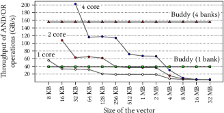
First, for each core count, the throughput of the Skylake drops with increasing size of the vector. This is expected as the working set will stop fitting in different levels of the on-chip cache as we move to the right on the x-axis. Second, as long the working set fits in some level of on-chip cache, running the operation with more cores provides higher throughput. Third, when the working set stops fitting in the on-chip caches (> 8MB per vector), the throughput with different core counts is roughly the same (5.8 GB/s of computed result). This is because, at this point, the throughput of the operation is strictly limited by the available memory bandwidth. Finally, for working sets larger than the cache size, Buddy significantly outperforms the baseline system. Even using only one bank, Buddy achieves a throughput of 38.92 GB/s, 6.7X better than the baseline. As modern DRAM chips have abundant bank-level parallelism, Buddy can achieve much higher throughput by using more banks (e.g., 26.8X better throughput with 4 banks, compared to the baseline). In fact, while the throughput of bitwise operations in existing systems is limited by the memory bandwidth, the throughput enabled by Buddy scales with the number of banks in the system.
Table 6.2 shows the throughput and energy results different bitwise operations for the 32MB input. We estimate energy for DDR3-1333 using the Rambus model [178]. Our energy numbers only include the DRAM and channel energy, and does not include the energy spent at the CPU and caches. For Buddy, some activate operations have rise multiple wordlines and hence will consume higher energy. To account for this, we increase the energy of the activate operation by 22% for each additional wordline raised. As a result, a triple-row activation will consume 44% more energy than a regular activation.
| Operation | Throughput (GB/s) | Energy (nJ) | ||||
|---|---|---|---|---|---|---|
| Base | Buddy | () | Base | Buddy | () | |
| not | 7.7 | 77.8 | 10.1X | 749.6 | 12.6 | 59.5X |
| and/or | 5.8 | 38.9 | 6.7X | 1102.8 | 25.1 | 43.9X |
| nand/nor | 5.8 | 31.1 | 5.3X | 1102.8 | 31.4 | 35.1X |
| xor/xnor | 5.8 | 22.2 | 3.8X | 1102.8 | 44.0 | 25.1X |
In summary, across all bitwise operations, Buddy reduces energy consumption by at least 25.1X and up to 59.5X compared to the baseline, and with just one bank, Buddy improves the throughput by at least 3.8X and up to 10.1X compared to the baseline. In the following section, we demonstrate the benefits of Buddy in some real-world applications.
6.6 Effect on Real-world Applications
To demonstrate the benefits of Buddy on real-world applications, we implement Buddy in the Gem5 [34] simulator. We implement the new Buddy instructions using the pseudo instruction framework in Gem5. We simulate an out-of-order, 4 GHz processor with 32 KB L1 D-cache and I-cache, with a shared 2 MB L2 cache. All caches use a 64B cache line size. We model a 1-channel, 1-rank, DDR4-2400 main memory. In Section 6.6.1, we first show that Buddy can significantly improve the performance of an in-memory bitmap index. In Section 6.6.2, we show that Buddy generally makes bitmaps more attractive for various set operations compared to traditional red-black trees. In Section 7.3.3, we discuss other potential applications that can benefit from Buddy.
6.6.1 Bitmap Indices
Bitmap indices are an alternative to traditional B-tree indices for databases. Compared to B-trees, bitmap indices can 1) consume less space, and 2) improve performance of certain queries. There are several real-world implementations of bitmap indices for databases (e.g., Oracle [165], Redis [10], Fastbit [5], rlite [11]). Several real applications (e.g., Spool [12], Belly [1], bitmapist [2], Audience Insights [59]) use bitmap indices for fast analytics.
Bitmap indices rely on fast bitwise operations on large bit vectors to achieve high performance. Therefore, Buddy can accelerate operations on bitmap indices, thereby improving overall application performance.
To demonstrate this benefit, we use the following workload representative of many applications. The application uses bitmap indices to track users’ characteristics (e.g., gender, premium) and activities (e.g., did the user log in to the website on day ’X’?) for users. The applications then uses bitwise operations on these bitmaps to answer several different queries. Our workload runs the following query: “How many unique users were active every week for the past weeks? and How many premium users were active each of the past weeks?” Executing this query requires 6 bitwise or, 2-1 bitwise and, and +1 bitcount operations.
The size of each bitmap (and hence each bitwise operation) depends on the number of users. For instance, a reasonably large application that has 8 million users will require each bitmap to be around 1 MB. Hence, these operations can easily be accelerated using Buddy (the bitcount operations are performed by the CPU). Figure 6.7 shows the execution time of the baseline and Buddy for the above experiment for various values of (number of users) and (number of days).
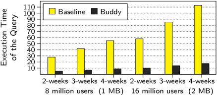
We draw two conclusions. First, as each query has bitwise operations and each bitwise operation takes time, the execution time of the query increases with increasing value . Second, Buddy significantly reduces the query execution time by 6X (on average) compared to the baseline.
While we demonstrate the benefits of Buddy using one query, as all bitmap index queries involve several bitwise operations, Buddy will provide similar performance benefits for any application using bitmap indices.
6.6.2 Bit Vectors vs. Red-Black Trees
A set data structure is widely used in many algorithms. Many libraries (e.g., C++ Standard Template Library [4]), use red-black trees [81] (RB-trees) to implement a set. While RB-trees are efficient when the domain of elements is very large, when the domain is limited, a set can be implemented using a bit vector. Bit vectors offer constant time insert and lookup as opposed to RB-trees, which consume time for both operations. However, with bit vectors, set operations like union, intersection, and difference have to operate on the entire bit vector, regardless of whether the elements are actually present in the set. As a result, for these operations, depending on the number of elements actually present in each set, bit vectors may outperform or perform worse than a RB-trees. With support for fast bulk bitwise operations, we show that Buddy significantly shifts the trade-off spectrum in favor of bit vectors.
To demonstrate this, we compare the performance of union, intersection, and difference operations using three implementations: RB-tree, bit vectors with SSE optimization (Bitset), and bit vectors with Buddy. We run a microbenchmark that performs each operation on 15 sets and stores the result in an output set. Each set can contain elements between 1 and 524288 (). Therefore, the bit vector approaches requires 64 KB to represent each set. For each operation, we vary the number of elements present in the input sets. Figure 6.8 shows the results of this experiment. The figure plots the execution time for each implementation normalized to RB-tree.
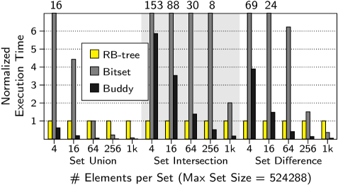
We draw three conclusions. First, by enabling much higher throughput for bitwise operations, Buddy outperforms the baseline bitset on all the experiments. Second, as expected, when the number of elements in each set is very small (16 out of 524288), RB-Tree performs better than the bit vector based implementations. Third, even when each set contains only 1024 (out of 524288) elements, Buddy significantly outperforms RB-Tree.
In summary, by performing bulk bitwise operations efficiently and with much higher throughput compared to existing systems, Buddy makes a bit-vector-based implementation of a set more attractive in scenarios where red-black trees previously outperformed bit vectors.
6.6.3 Other Applications
Cryptography.
Many encryption algorithms in cryptography heavily use bitwise operations (e.g., XOR) [223, 86, 148]. The Buddy support for fast and efficient bitwise operations can i) boost the performance of existing encryption algorithms, and ii) enable new encryption algorithms with high throughput and efficiency.
DNA Sequence Mapping.
DNA sequence mapping has become an important problem, with applications in personalized medicine. Most algorithms [189] rely on identifying the locations where a small DNA sub-string occurs in the reference gnome. As the reference gnome is large, a number of pre-processing algorithms [139, 184, 233, 239] have been proposed to speedup this operation. Based on a prior work [179], we believe bit vectors with support for fast bitwise operations using Buddy can enable an efficient filtering mechanism.
Approximate Statistics.
Certain large systems employ probabilistic data structures to improve the efficiency of maintaining statistics [37]. Many such structures (e.g., Bloom filters) rely on bitwise operations to achieve high efficiency. By improving the throughput of bitwise operations, Buddy can further improve the efficiency of such data structures, and potentially enable the design of new data structures in this space.
6.7 Related Work
There are several prior works that aim to enable efficient computation near memory. In this section, we qualitatively compare Buddy to these prior works.
Some recent patents [23, 22] from Mikamonu describe an architecture that employs a DRAM organization with 3T-1C cells and additional logic to perform NAND/NOR operations on the data inside DRAM. While this architecture can perform bitwise operations inside DRAM, it incurs significant additional cost to the DRAM array due to the extra transistors, and hence reduces overall memory density/capacity. In contrast, Buddy exploits existing DRAM operation to perform bitwise operations efficiently inside DRAM. As a result, it incurs much lower cost compared to the Mikamonu architecture.
One main source of memory inefficiency in existing systems is data movement. Data has to travel off-chip buses and multiple levels of caches before reaching the CPU. To avoid this data movement, many works (e.g., NON-VON Database Machine [14], DIVA [61], Terasys [78], Computational RAM [66], FlexRAM [117, 70], EXECUBE [127], Active Pages [166], Intelligent RAM [169], Logic-in-Memory Computer [209]) have proposed mechanisms and models to add processing logic close to memory. The idea is to integrate memory and CPU on the same chip by designing the CPU using the memory process technology. While the reduced data movement allows these approaches to enable low-latency, high-bandwidth, and low-energy data communication, they suffer from two key shortcomings. First, this approach of integrating processor on the same chip as memory significantly deviates from existing designs, and as a result, increases the overall cost of the system. Second, DRAM vendors use a high-density process to minimize cost-per-bit. Unfortunately, high-density DRAM process is not suitable for building high-speed logic [169]. As a result, this approach is not suitable for building a general purpose processor near memory. In contrast, we restrict our focus to bitwise operations, and propose a mechanism to perform them efficiently inside DRAM with low cost.
Some recent DRAM architectures [145, 107, 6] use 3D-stacking technology to stack multiple DRAM chips on top of the processor chip or a separate logic layer. These architectures offer much higher bandwidth to the logic layer compared to traditional off-chip interfaces. This enables an opportunity to offload some computation to the logic layer, thereby improving performance. In fact, many recent works have proposed mechanisms to improve and exploit such architectures (e.g., [21, 20, 244, 69, 82, 255, 218, 95, 75, 153, 90, 74, 68, 28, 24, 135]). Unfortunately, despite enabling higher bandwidth compared to off-chip memory, such 3D-stacked architectures are still require data to be transferred outside the DRAM chip, and hence can be bandwidth-limited. However, since Buddy can be integrated easily with such architectures, we believe the logic layer in such 3D architectures should be used to implement more complex operations, while Buddy can be used to efficiently implement bitwise logical operations at low cost.
6.8 Summary
In this chapter, we introduced Buddy, a new DRAM substrate that performs row-wide bitwise operations using DRAM technology. Specifically, we proposed two component mechanisms. First, we showed that simultaneous activation of three DRAM rows that are connected to the same set of sense amplifiers can be used to efficiently perform AND/OR operations. Second, we showed that the inverters present in each sense amplifier can be used to efficiently implement NOT operations. With these two mechanisms, Buddy can perform any bulk bitwise logical operation quickly and efficiently within DRAM. Our evaluations show that Buddy enables an order-of-magnitude improvement in the throughput of bitwise operations. This improvement directly translates to significant performance improvement in the evaluated real-world applications. Buddy is generally applicable to any memory architecture that uses DRAM technology, and we believe that the support for fast and efficient bulk bitwise operations can enable better design of applications that result in large improvements in performance and efficiency.
Chapter 7 Gather-Scatter DRAM
Originally published as “Gather-Scatter DRAM: In-DRAM Address Translation to Improve the Spatial Locality of Non-unit Strided Accesses” in the International Symposium on Microarchitecture, 2015 [193]
In this chapter, we shift our focus to the problem of non-unit strided access patterns. As described in Section 2.2.1, such access patterns present themselves in many important applications such as in-memory databases, scientific computation, etc. As illustrated in that section, non-unit strided access patterns exhibit low spatial locality. In existing memory systems that are optimized to access and store wide cache lines, such access patterns result in high inefficiency.
The problem presents itself at two levels. First, commodity DRAM modules are designed to supply wide contiguous cache lines. As a result, the cache lines fetched by the memory controller are only partially useful—i.e., they contain many values that do not belong to the strided access pattern. This results in both high latency and wasted memory bandwidth. Second, modern caches are optimized to store cache lines. Consequently, even the caches have to store values that do not belong to the strided access. While this results in inefficient use of the on-chip cache space, this also negatively affects SIMD optimizations on strided data. The application must first gather (using software or hardware) the values of the strided access in a single vector register before it can perform any SIMD operation. Unfortunately, this gather involves multiple physical cache lines, and hence is a long-latency operation.
Given the importance of strided access patterns, several prior works (e.g., Impulse [39, 245], Adaptive/Dynamic Granularity Memory Systems [242, 243]) have proposed solutions to improve the performance of strided accesses. Unfortunately, prior works [39, 242, 243] require the off-chip memory interface to support fine-grained memory accesses [252, 19, 18, 231, 38] and, in some cases, a sectored cache [142, 197]. These approaches significantly increase the cost of the memory interface and the cache tag store, and potentially lower the utilization of off-chip memory bandwidth and on-chip cache space. We discuss these prior works in more detail in Section 7.5.
Our goal is to design a mechanism that 1) improves the performance (cache hit rate and memory bandwidth consumption) of strided accesses, and 2) works with commodity DRAM modules and traditional non-sectored caches with very few changes. To this end, we first restrict our focus to power-of-2 strided access patterns and propose the Gather-Scatter DRAM (GS-DRAM), a substrate that allows the memory controller to gather or scatter data with any power-of-2 stride efficiently with very few changes to the DRAM module. In the following sections, we describe GS-DRAM in detail.
7.1 The Gather-Scatter DRAM
For the purpose of understanding the problems in existing systems and understanding the challenges in designing in GS-DRAM, we use the following database example. The database consists of a single table with four fields. We assume that each tuple of the database fits in a cache line. Figure 7.1 illustrates the two problems of accessing just the first field of the table. As shown in the figure, this query results in high latency, and wasted bandwidth and cache space.
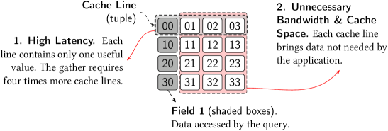
Our goal is to design a DRAM substrate that will enable the processor to access a field of the table (stored in tuple-major order) across all tuples, without incurring the penalties of existing interfaces. More specifically, if the memory controller wants to read the first field of the first four tuples of the table, it must be able to issue a single command that fetches the following gathered cache line: . At the same time, the controller must be able to read a tuple from memory (e.g., ) with a single command.
Our mechanism is based on the fact that modern DRAM modules consist of many DRAM chips. As described in Section 4.3, to achieve high bandwidth, multiple chips are grouped together to form a rank, and all chips within a rank operate in unison. Our idea is to enable the controller to access multiple values from a strided access from different chips within the rank with a single command. However, there are two challenges in implementing this idea. For the purpose of describing the challenges and our mechanism, we assume that each rank consist of four DRAM chips. However, GS-DRAM is general and can be extended to any rank with power-of-2 number of DRAM chips.
7.1.1 Challenges in Designing GS-DRAM
Figure 7.2 shows the two challenges. We assume that the first four tuples of the table are stored from the beginning of a DRAM row. Since each tuple maps to a single cache line, the data of each tuple is split across all four chips. The mapping between different segments of the cache line and the chips is controlled by the memory controller. Based on the mapping scheme described in Section 4.3, the 8 bytes of each cache line (i.e., the field of each tuple) is mapped to the chip.
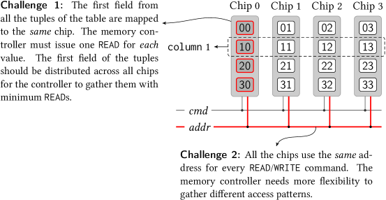
Challenge 1: Reducing chip conflicts. The simple mapping mechanism maps the first field of all the tuples to Chip 0. Since each chip can send out only one field (8 bytes) per READ operation, gathering the first field of the four tuples will necessarily require four READs. In a general scenario, different pieces of data that are required by a strided access pattern will be mapped to different chips. When two such pieces of data are mapped to the same chip, it results in what we call a chip conflict. Chip conflicts increase the number of READs required to gather all the values of a strided access pattern. Therefore, we have to map the data structure to the chips in a manner that minimizes the number of chip conflicts for target access patterns.
Challenge 2: Communicating the access pattern to the module. As shown in Figure 7.2, when a column command is sent to a rank, all the chips select the same column from the activated row and send out the data. If the memory controller needs to access the first tuple of the table and the first field of the four tuples each with a single READ operation, we need to break this constraint and allow the memory controller to potentially read different columns from different chips using a single READ command. One naive way of achieving this flexibility is to use multiple address buses, one for each chip. Unfortunately, this approach is very costly as it significantly increases the pin count of the memory channel. Therefore, we need a simple and low cost mechanism to allow the memory controller to efficiently communicate different access patterns to the DRAM module.
In the following sections, we propose a simple mechanism to address the above challenges with specific focus on power-of-2 strided access patterns. While non-power-of-2 strides (e.g., odd strides) pose some additional challenges (e.g., alignment), a similar approach can be used to support non-power-of-2 strides as well.
7.1.2 Column ID-based Data Shuffling
To address challenge 1, i.e., to minimize chip conflicts, the memory controller must employ a mapping scheme that distributes data of each cache line to different DRAM chips with the following three goals. First, the mapping scheme should be able to minimize chip conflicts for a number of access patterns. Second, the memory controller must be able to succinctly communicate an access pattern along with a column command to the DRAM module. Third, once the different parts of the cache line are read from different chips, the memory controller must be able to quickly assemble the cache line. Unfortunately, these goals are conflicting.
While a simple mapping scheme enables the controller to assemble a cache line by concatenating the data received from different chips, this scheme incurs a large number of chip conflicts for many frequently occurring access patterns (e.g., any power-of-2 stride > 1). On the other hand, pseudo-random mapping schemes [180] potentially incur a small number of conflicts for almost any access pattern. Unfortunately, such pseudo-random mapping schemes have two shortcomings. First, for any cache line access, the memory controller must compute which column of data to access from each chip and communicate this information to the chips along with the column command. With a pseudo random interleaving, this communication may require a separate address bus for each chip, which would significantly increase the cost of the memory channel. Second, after reading the data, the memory controller must spend more time assembling the cache line, increasing the overall latency of the READ operation.
We propose a simple column ID-based data shuffling mechanism that achieves a sweet spot by restricting our focus to power-of-2 strided access patterns. Our shuffling mechanism is similar to a butterfly network [56], and is implemented in the memory controller. To map the data of the cache line with column address to different chips, the memory controller inspects the least significant bits (LSB) of . Based on these bits, the controller uses stages of shuffling. Figure 7.3 shows an example of a 2-stage shuffling mechanism. In Stage 1 (Figure 7.3), if the LSB is set, our mechanism groups adjacent 8-byte values in the cache line into pairs and swaps the values within each pair. In Stage 2 (Figure 7.3), if the second LSB is set, our mechanism groups the 8-byte values in the cache line into quadruplets, and swaps the adjacent pairs of values. The mechanism proceeds similarly into the higher levels, doubling the size of the group of values swapped in each higher stage. The shuffling mechanism can be enabled only for those data structures that require our mechanism. Section 7.2.3 discusses this in more detail.
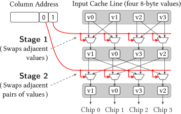
With this simple multi-stage shuffling mechanism, the memory controller can map data to DRAM chips such that any power-of-2 strided access pattern incurs minimal chip conflicts for values within a single DRAM row.
7.1.3 Pattern ID: Low-cost Column Translation
The second challenge is to enable the memory controller to flexibly access different column addresses from different DRAM chips using a single READ command. To this end, we propose a mechanism wherein the controller associates a pattern ID with each access pattern. It provides this pattern ID with each column command. Each DRAM chip then independently computes a new column address based on 1) the issued column address, 2) the chip ID, and 3) the pattern ID. We refer to this mechanism as column translation.
Figure 7.4 shows the column translation logic for a single chip. As shown in the figure, our mechanism requires only two bitwise operations per chip to compute the new column address. More specifically, the output column address for each chip is given by (Chip ID & Pattern ID) Column ID, where Column ID is the column address provided by the memory controller. In addition to the logic to perform these simple bitwise operations, our mechanism requires 1) a register per chip to store the chip ID, and 2) a multiplexer to enable the address translation only for column commands. While our column translation logic can be combined with the column selection logic already present within each chip, our mechanism can also be implemented within the DRAM module with no changes to the DRAM chips.
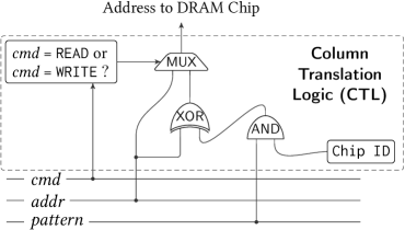
Combining this pattern-ID-based column translation mechanism with the column-ID-based data shuffling mechanism, the memory controller can gather or scatter any power-of-two strided access pattern with no waste in memory bandwidth.
7.1.4 GS-DRAM: Putting It All Together
Figure 7.5 shows the full overview of our GS-DRAM substrate. The figure shows how the first four tuples of our example table are mapped to the DRAM chips using our data shuffling mechanism. The first tuple (column ID 0) undergoes no shuffling as the two LSBs of the column ID are both 0 (see Figure 7.3). For the second tuple (column ID 1), the adjacent values within each pairs of values are swapped (Figure 7.3, Stage 1). Similarly, for the third tuple (column ID 2), adjacent pair of values are swapped (Figure 7.3, Stage 2). For the fourth tuple (column ID 3), since the two LSBs of the column ID are both 1, both stages of the shuffling scheme are enabled (Figure 7.3, Stages 1 and 2). As shown in shaded boxes in Figure 7.5, the first field of the four tuples (i.e., ) are mapped to different chips, allowing the memory controller to read them with a single READ command. The same is true for the other fields of the table as well (e.g., )
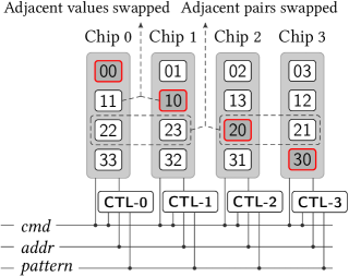
The figure also shows the per-chip column translation logic. To read a specific tuple from the table, the memory controller simply issues a READ command with pattern ID 0 and an appropriate column address. For example, when the memory controller issues the READ for column ID 2 and pattern 0, the four chips return the data corresponding to the columns (2 2 2 2), which is the data in the third tuple of the table (i.e., ). In other words, pattern ID 0 allows the memory controller to perform the default read operation. Hence, we refer to pattern ID 0 as the default pattern.
On the other hand, if the memory controller issues a READ for column ID 0 and pattern 3, the four chips return the data corresponding to columns (0 1 2 3), which precisely maps to the first field of the table. Similarly, the other fields of the first four tuples can be read from the database by varying the column ID with pattern 3.
7.1.5 GS-DRAM Parameters
GS-DRAM has three main parameters: 1) the number of chips in each module, 2) the number of shuffling stages in the data shuffling mechanism, and 3) the number of bits of pattern ID. While the number of chips determines the size of each cache line, the other two parameters determine the set of access patterns that can be efficiently gathered by GS-DRAM. We use the term GS-DRAMc,s,p to denote a GS-DRAM with chips, stages of shuffling, and bits of pattern ID.
Figure 7.6 shows all cache lines that can be gathered by GS-DRAM4,2,2, with the four possible patterns for column IDs 0 through 3. For each pattern ID and column ID combination, the figure shows the index of the four values within the row buffer that are retrieved from the DRAM module. As shown, pattern 0 retrieves contiguous values. Pattern 1 retrieves every other value (stride = 2). Pattern 2 has a dual stride of (1,7). Pattern 3 retrieves every 4th value (stride = 4). In general, pattern gathers data with a stride .
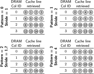
While we showed a use case for pattern 3 (in our example), we envision use-cases for other patterns as well. Pattern 1, for instance, can be useful for data structures like key-value stores. Assuming an 8-byte key and an 8-byte value, the cache line (Patt 0, Col 0) corresponds to the first two key-value pairs. However the cache line (Patt 1, Col 0) corresponds to the first four keys, and (Patt 1, Col 1) corresponds to the first four values. Similarly, pattern 2 can be use to fetch odd-even pairs of fields from a data structure where each object has 8 fields.
Our mechanism is general. For instance, with GS-DRAM8,3,3 (i.e., 8 chips, 3 shuffling stages, and 3-bit pattern ID), the memory controller can access data with seven different patterns. Section 7.4 discusses other simple extensions to our approach to enable more fine-grained gather access patterns, and larger strides.
7.1.6 Ease of Implementing GS-DRAM
In Section 7.3, we will show that GS-DRAM has compelling performance and energy benefits compared to existing DRAM interfaces. These benefits are augmented by the fact that GS-DRAM is simple to implement. First, our data shuffling mechanism is simple and has low latency. Each stage involves only data swapping and takes at most one processor cycle. Our evaluations use GS-DRAM8,3,3, thereby incurring 3 cycles of additional latency to shuffle/unshuffle data for each DRAM write/read. Second, for GS-DRAM∗,∗,p, the column translation logic requires only two p-bit bitwise operations, a p-bit register to store the chip ID, and a p-bit multiplexer. In fact, this mechanism can be implemented as part of the DRAM module without any changes to the DRAM chips themselves. Finally, third, GS-DRAM requires the memory controller to communicate only k bits of pattern ID to the DRAM module, adding only a few pins to each channel. In fact, the column command in existing DDR DRAM interfaces already has a few spare address pins that can potentially be used by the memory controller to communicate the pattern ID (e.g., DDR4 has two spare address pins for column commands [111]).
7.2 End-to-end System Design
In this section, we discuss the support required from the rest of the system stack to exploit the GS-DRAM substrate. We propose a mechanism that leverages support from different layers of the system stack to exploit GS-DRAM: 1) on-chip caches, 2) the instruction set architecture, and 3) software. It is also possible for the processor to dynamically identify different access patterns present in an application and exploit GS-DRAM to accelerate such patterns transparently to the application. As our goal in this work is to demonstrate the benefits of GS-DRAM, we leave the design of such an automatic mechanism for future work. The following sections assume a GS-DRAM∗,∗,p, i.e., a p-bit pattern ID.
7.2.1 On-Chip Cache Support
Our mechanism introduces two problems with respect to on-chip cache management. First, when the memory controller gathers a cache line from a non-zero pattern ID, the values in the cache line are not contiguously stored in physical memory. For instance, in our example (Figure 7.1), although the controller can fetch the first field of the first four tuples of the table with a single READ, the first field of the table is not stored contiguously in physical memory. Second, two cache lines belonging to different patterns may have a partial overlap. In our example (Figure 7.1), if the memory controller reads the first tuple (pattern ID = 0, column ID = 0) and the first field of the first four tuples (pattern ID = 3, column ID = 0), the two resulting cache lines have a common value (the first field of the first tuple, i.e., ).
One simple way to avoid these problems is to store the individual values of the gathered data in different physical cache lines by employing a sectored cache [142] (for example). However, with the off-chip interface to DRAM operating at a wider-than-sector (i.e., a full cache line) granularity, such a design will increase the complexity of the cache-DRAM interface. For example, writebacks may require read-modify-writes as the processor may not have the entire cache line. More importantly, a mechanism that does not store the gathered values in the same cache line cannot extract the full benefits of SIMD optimizations because values that are required by a single SIMD operation would now be stored in multiple physical cache lines. Therefore, we propose a simple mechanism that stores each gathered cache line from DRAM in a single physical cache line in the on-chip cache. Our mechanism has two aspects.
1. Identifying non-contiguous cache lines. When a non-contiguous cache line is stored in the cache, the cache controller needs a mechanism to identify the cache line. We observe that, in our proposed system, each cache line can be uniquely identified using the cache line address and the pattern ID with which it was fetched from DRAM. Therefore, we extend each cache line tag in the cache tag store with additional bits to store the pattern ID of the corresponding cache line.
2. Maintaining cache coherence. The presence of overlapping cache lines has two implications on coherence. First, before fetching a cache line from DRAM, the controller must check if there are any dirty cache lines in the cache which have a partial overlap with the cache line being fetched. Second, when a value is modified by the processor, in addition to invalidating the modified cache line from the other caches, the processor must also invalidate all other cache lines that contain the value that is being modified. With a number of different available patterns, this operation can be a complex and costly.
Fortunately, we observe that many applications that use strided accesses require only two pattern IDs per data structure, the default pattern and one other pattern ID. Thus, as a trade-off to simplify cache coherence, we restrict each data structure to use only the zero pattern and one other pattern ID. To implement this constraint, we associate each virtual page with an additional -bit pattern ID. Any access to a cache line within the page can use either the zero pattern or the page’s pattern ID. If multiple virtual pages are mapped to the same physical page, the OS must ensure that the same alternate pattern ID is used for all mappings.
Before fetching a cache line from DRAM with a pattern, the memory controller must only look for dirty cache lines from the other pattern. Since all these cache lines belong to the same DRAM row, this operation is fast and can be accelerated using simple structures like the Dirty-Block Index (described in Chapter 8 of this thesis). Similarly, when the processor needs to modify a shared cache line, our mechanism piggybacks the other pattern ID of the page along with the read-exclusive coherence request. Each cache controller then locally invalidates the cache lines from the other pattern ID that overlap with the cache line being modified. For GS-DRAMc,∗,∗, our mechanism requires additional invalidations for each read-exclusive request.
7.2.2 Instruction Set Architecture Support
To enable software to communicate strided access patterns to the
processor, we introduce a new variant of the load and
store instructions, called pattload and
pattstore, that allow the code to specify the pattern
ID. These instructions takes the following
form:
pattload reg, addr, patt
pattstore reg, addr, patt
where reg is the source or destination register (depending on the instruction type), addr is the address of the data, and patt is the pattern ID.
To execute a pattload or pattstore, the processor first splits the addr field into two parts: the cache line address (caddr), and the offset within the cache line (offset). Then the processor sends out a request for the cache line with address-pattern combination (caddr, patt). If the cache line is present in the on-chip cache, it is sent to the processor. Otherwise, the request reaches the memory controller. The memory controller identifies the row address and the column address from caddr and issues a READ command for a cache line with pattern ID patt. If the memory controller interleaves cache lines across multiple channels (or ranks), then it must access the corresponding cache line within each channel (or rank) and interleave the data from different channels appropriately before obtaining the required cache line. The cache line is then stored in the on-chip cache and is also sent to the processor. After receiving the cache line, the processor reads or updates the data at the offset to or from the destination or source register (reg).
Note that architectures like x86 allow instructions to directly operate on memory by using different addressing modes to specify memory operands [7]. For such architectures, common addressing modes may be augmented with a pattern ID field, or instruction prefixes may be employed to specify the pattern.
7.2.3 System and Application Software Support
Our mechanism requires two pieces of information from the software for each data structure: 1) whether the data structure requires the memory controller to use the shuffling mechanism (Section 7.1.2) (we refer to this as the shuffle flag), and 2) the alternate pattern ID (Section 7.1.3) with which the application will access the data structure. To enable the application to specify this information, we propose a new variant of the malloc system call, called pattmalloc, which includes two additional parameters: the shuffle flag, and the pattern ID. When the OS allocates virtual pages for a pattmalloc, it also updates the page tables with the shuffle flag and the alternate pattern ID for those pages.
Once the data structure is allocated with pattmalloc, the application can use the pattload or pattstore instruction to access the data structure efficiently with both the zero pattern and the alternate access pattern. While we can envision automating this process using a compiler optimization, we do not explore that path in this thesis. Figure 7.7 shows an example piece of code before and after our optimization. The original code (line 5) allocates an array of 512 objects (each object with eight 8-byte fields) and computes the sum of the first field of all the objects (lines 8 and 9). The figure highlights the key benefit of our approach.
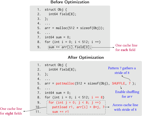
In the program without our optimization (Figure 7.7, left), each iteration of the loop (line 9) fetches a different cache line. As a result, the entire loop accesses 512 different cache lines. On the other hand, with our optimization (Figure 7.7, right), the program first allocates memory for the array using pattmalloc (line 5), with the shuffle flag enabled and an alternate pattern ID = 7 (i.e., stride of 8). The program then breaks the loop into two parts. Each iteration of the outer loop (line 8) fetches a single strided cache line that contains only values from the first field. The loop skips the other fields (i += 8). The inner loop (lines 9-11) iterates over values within each strided cache line. In the first iteration of the inner loop, the pattload instruction with pattern ID 7 fetches a cache line with a stride of 8. As a result, the remaining seven iterations of the inner loop result in cache hits. Consequently, with our optimization, the entire loop accesses only 64 cache lines. As we will show in our evaluations, this reduction in the number of accessed cache lines directly translates to reduction in latency, bandwidth consumption, and cache capacity consumption, thereby improving overall performance.
7.2.4 Hardware Cost
In this section, we quantify the changes required by GS-DRAM, specifically GS-DRAM8,3,3 (Section 7.1.5), to various hardware components. On the DRAM side, first, our mechanism requires the addition of the column translation logic (CTL) for each DRAM chip. Each CTL requires a 3-bit register for the Chip ID, a 3-bit bitwise AND gate, a 3-bit bitwise XOR gate and a 3-bit bitwise multiplexer. Even for a commodity DRAM module with 8 chips, the overall cost is roughly 72 logic gates and 24 bits of register storage, which is negligible compared to the logic already present in a DRAM module. Second, our mechanism requires a few additional pins on the DRAM interface to communicate the pattern ID. However, existing DRAM interfaces already have some spare address bits, which can be used to communicate part of the pattern ID. Using this approach, a 3-bit pattern ID requires only one additional pin for DDR4 [111].
On the processor side, first, our mechanism requires the controller to implement the shuffling logic. Second, our mechanism augments each cache tag entry with the pattern ID. Each page table entry and TLB entry stores the shuffle flag and the alternate pattern ID for the corresponding page (Section 7.2.1). For a 3-bit pattern ID, the cost of this addition is less than 0.6% of the cache size. Finally, the processor must implement the pattload and pattstore instructions, and the state machine for invalidating additional cache lines on read-exclusive coherence requests. The operation of pattload/pattstore is not very different from that of a regular load/store instruction. Therefore, we expect the implementation of these new instructions to be simple. Similarly, on a write, our mechanism has to check only eight cache lines (for GS-DRAM with 8 chips) for possible overlap with the modified cache line. Therefore, we expect the invalidation state machine to be relatively simple. Note that a similar state machine has been used to keep data coherent in a virtually-indexed physically-tagged cache in the presence of synonyms [15].
7.3 Applications and Evaluations
To quantitatively evaluate the benefits of GS-DRAM, we implement our framework in the Gem5 simulator [34], on top of the x86 architecture. We implement the pattload instruction by modifying the behavior of the prefetch instruction to gather with a specific pattern into either the rax register (8 bytes) or the xmm0 register (16 bytes). None of our evaluated applications required the pattstore instruction. Table 7.1 lists the main parameters of the simulated system. All caches uniformly use 64-byte cache lines. While we envision several applications to benefit from our framework, in this section, we primarily discuss and evaluate two applications: 1) an in-memory database workload, and 2) general matrix-matrix multiplication workload.
| Processor | 1-2 cores, x86, in-order, 4 GHz |
|---|---|
| L1-D Cache | Private, 32 KB, 8-way associative, LRU policy |
| L1-I Cache | Private, 32 KB, 8-way associative, LRU policy |
| L2 Cache | Shared, 2 MB, 8-way associative, LRU policy |
| Memory | DDR3-1600, 1 channel, 1 rank, 8 banks |
| Open row, FR-FCFS [182, 256], GS-DRAM8,3,3 |
7.3.1 In-Memory Databases
In-memory databases (IMDB) (e.g., [198, 116, 80]) provide significantly higher performance than traditional disk-oriented databases. Similar to any other database, an IMDB may support two kinds of queries: transactions, which access many fields from a few tuples, and analytics, which access one or few fields from many tuples. As a result, the storage model used for the database tables heavily impacts the performance of transactions and analytical queries. While a row-oriented organization (row store) is better for transactions, a column-oriented organization [210] (column store) is better for analytics. Increasing need for both fast transactions and fast real-time analytics has given rise to a new workload referred to as Hybrid Transaction/Analytical Processing (HTAP) [17]. In an HTAP workload, both transactions and analytical queries are run on the same version of the database. Unfortunately, neither the row store nor the column store provides the best performance for both transactions and analytics.
With our GS-DRAM framework, each database table can be stored as a row store in memory, but can be accessed at high performance both in the row-oriented access pattern and the field-oriented access pattern.111GS-DRAM requires the database to be structured (i.e., not have any variable length fields). This is fine for most high-performance IMDBs as they handle variable length fields using fixed size pointers for fast data retrieval [150, 84]. GS-DRAM will perform at least as well as the baseline for unstructured databases. Therefore, we expect GS-DRAM to provide the best of both row and column layouts for both kinds of queries. We demonstrate this potential benefit by comparing the performance of GS-DRAM with both a row store layout (Row Store) and a column store layout (Column Store) on three workloads: 1) a transaction-only workload, 2) an analytics-only workload, and 3) an HTAP workload. For our experiments, we assume an IMDB with a single table with one million tuples and no use of compression. Each tuple contains eight 8-byte fields, and fits exactly in a 64B cache line. (Our mechanism naturally extends to any table with power-of-2 tuple size.)
Transaction workload. For this workload, each transaction operates on a randomly-chosen tuple. All transactions access , , and fields of the tuple in the read-only, write-only, and read-write mode, respectively. Figure 7.8 compares the performance (execution time) of GS-DRAM, Row Store, and Column Store on the transaction workload for various values of , , and (x-axis). The workloads are sorted based on the total number of fields accessed by each transaction. For each mechanism, the figure plots the execution time for running 10000 transactions.
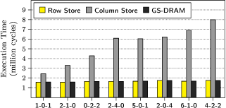
We draw three conclusions. First, as each transaction accesses only one tuple, it accesses only one cache line. Therefore, the performance of Row Store is almost the same regardless of the number of fields read/written by each transaction. Second, the performance of Column Store is worse than that of Row Store, and decreases with increasing number of fields. This is because Column Store accesses a different cache line for each field of a tuple accessed by a transaction, thereby causing a large number of memory accesses. Finally, as expected, GS-DRAM performs as well as Row Store and 3X (on average) better than Column Store for the transactions workload.
Analytics workload. For this workload, we measure the time taken to run a query that computes the sum of columns from the table. Figure 7.9 compares the performance of the three mechanisms on the analytics workload for and . The figure shows the performance of each mechanism without and with prefetching. We use a PC-based stride prefetcher [30] (with prefetching degree of 4 [205]) that prefetches data into the L2 cache. We draw several conclusions from the results.
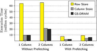
First, prefetching significantly improves the performance of all three mechanisms for both queries. This is expected as the analytics query has a uniform stride for all mechanisms, which can be easily detected by the prefetcher. Second, the performance of Row Store is roughly the same for both queries. This is because each tuple of the table fits in a single cache line and hence, the number of memory accesses for Row Store is the same for both queries (with and without prefetching). Third, the execution time of Column Store increases with more fields. This is expected as Column Store needs to fetch more cache lines when accessing more fields from the table. Regardless, Column Store significantly outperforms Row Store for both queries, as it causes far fewer cache line fetches compared to Row Store. Finally, GS-DRAM, by gathering the columns from the table as efficiently as Column Store, performs similarly to Column Store and significantly better than Row Store both without and with prefetching (2X on average).
HTAP workload. For this workload, we run one analytics thread and one transactions thread concurrently on the same system operating on the same table. The analytics thread computes the sum of a single column, whereas the transactions thread runs transactions (on randomly chosen tuples with one read-only and one write-only field). The transaction thread runs until the analytics thread completes. We measure 1) the time taken to complete the analytics query, and 2) the throughput of the transactions thread. Figures 7.10(a) and 7.10(b) plot these results, without and with prefetching.

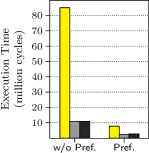
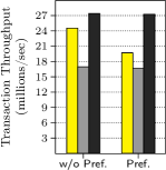
First, for analytics, prefetching significantly improves performance for all three mechanisms. GS-DRAM performs as well as Column Store. Second, for transactions, we find that GS-DRAM not only outperforms Column Store, in terms of transaction throughput, but it also performs better than Row Store. We traced this effect back to inter-thread contention for main memory bandwidth, a well-studied problem (e.g., [213, 76, 124, 156, 157, 123]). The FR-FCFS [182, 256] memory scheduler prioritizes requests that hit in the row buffer. With Row Store, the analytics thread accesses all the cache lines in a DRAM row, thereby starving requests of the transaction thread to the same bank (similar to a memory performance hog program described in [154]). In contrast, by fetching just the required field, GS-DRAM accesses 8 times fewer cache lines per row. As a result, it stalls the transaction thread for much smaller amount of time, leading to higher transaction throughput than Row Store. The problem becomes worse for Row Store with prefetching, since the prefetcher makes the analytics thread run even faster, thereby consuming a larger fraction of the memory bandwidth.
Energy. We use McPAT [140] and DRAMPower [43, 42] (integrated with Gem5 [34]) to estimate the processor and DRAM energy consumption of the three mechanisms. Our evaluations show that, for transactions, GS-DRAM consumes similar energy to Row Store and 2.1X lower than Column Store. For analytics (with prefetching enabled), GS-DRAM consumes similar energy to Column Store and 2.4X lower energy (4X without prefetching) than Row Store. (As different mechanisms perform different amounts of work for the HTAP workload, we do not compare energy for this workload.) The energy benefits of GS-DRAM over prior approaches come from 1) lower overall processor energy consumption due to reduced execution time, and 2) lower DRAM energy consumption due to significantly fewer memory accesses.
Figure 7.11 summarizes the performance and energy benefits of GS-DRAM compared to Row Store and Column Store for the transactions and the analytics workloads. We conclude that GS-DRAM provides the best of both the layouts.

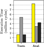
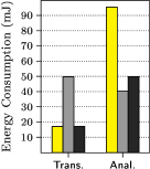
7.3.2 Scientific Computation: GEMM
General Matrix-Matrix (GEMM) multiplication is an important kernel in many scientific computations. When two matrices and are multiplied, the matrix is accessed in the row-major order, whereas the matrix is accessed in the column-major order. If both matrices are stored in row-major order, a naive algorithm will result in poor spatial locality for accesses to . To mitigate this problem, matrix libraries use two techniques. First, they split each matrix into smaller tiles, converting the reuses of matrix values into L1 cache hits. Second, they use SIMD instructions to speed up each vector dot product involved in the operation.
Unfortunately, even after tiling, values of a column of matrix are stored in different cache lines. As a result, to exploit SIMD, the software must gather the values of a column into a SIMD register. In contrast, GS-DRAM can read each tile of the matrix in the column-major order into the L1 cache such that each cache line contains values gathered from one column. As a result, GS-DRAM naturally enables SIMD operations, without requiring the software to gather data into SIMD registers.
Figure 7.12 plots the performance of GEMM with GS-DRAM and with the best tiled version normalized to a non-tiled version for different sizes () of the input matrices. We draw two conclusions. First, as the size of the matrices increases, tiling provides significant performance improvement by eliminating many memory references. Second, by seamlessly enabling SIMD operations, GS-DRAM improves the performance of GEMM multiplication by 10% on average compared to the best tiled baseline. Note that GS-DRAM achieves 10% improvement over a heavily-optimized tiled baseline that spends most of its time in the L1 cache.
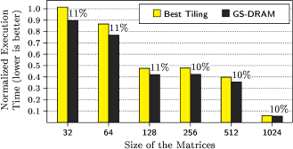
7.3.3 Other Applications
We envision GS-DRAM to benefit many other applications like key-value stores, graph processing, and graphics. Key-value stores have two main operations: insert and lookup. The insert operation benefits from both the key and value being in the same cache line. On the other hand, the lookup operation benefits from accessing a cache line that contains only keys. Similarly, in graph processing, operations that update individual nodes in the graph have different access patterns than those that traverse the graph. In graphics, multiple pieces of information (e.g., RGB values of pixels) may be packed into small objects. Different operations may access multiple values within an object or a single value across a large number of objects. The different access patterns exhibited by these applications have a regular stride and can benefit significantly from GS-DRAM.
7.4 Extensions to GS-DRAM
In this section, we describe three simple extensions to GS-DRAM: 1) programmable shuffling, 2) wider pattern IDs, and 3) intra-chip column translation. These extensions (together or individually) allow GS-DRAM to 1) express more patterns (e.g., larger strides), 2) gather or scatter data at a granularity smaller than 8 bytes, and 3) enable ECC support.
7.4.1 Programmable Shuffling
Although our shuffling mechanism uses the least significant bits of the column ID to control the shuffling stages, there are two simple ways of explicitly controlling which shuffling stages are active. First, we can use a shuffle mask to disable some stages. For example, the shuffle mask 10 disables swapping of adjacent values (Figure 7.3, Stage 1). Second, instead of using the least significant bits to control the shuffling stages, we can choose different combinations of bits (e.g., XOR of multiple sets of bits [226, 71]). To enable programmable shuffling, we add another parameter to GS-DRAM called the shuffling function, . For GS-DRAMc,s,p,f, the function takes a column ID as input and generates an -bit value that is used as the control input to the shuffling stages. The function can be application-specific, thereby optimizing GS-DRAM for each application.
7.4.2 Wider Pattern IDs
Although a wide pattern ID comes at additional cost, using a wider pattern ID allows the memory controller to express more access patterns. However, the column translation logic (CTL) performs a bitwise AND of the chip ID and the pattern ID to create a modifier for the column address. As a result, even if we use a wide pattern ID, a small chip ID disables the higher order bits of the pattern ID. Specifically, for GS-DRAMc,∗,p, if , the CTL uses only the least significant bits of the pattern ID. To enable wider pattern IDs, we propose to simply widen the chip ID used by the CTL by repeating the physical chip ID multiple times. For instance, with 8 chips and a 6-bit pattern ID, the chip ID used by CTL for chip will be 011-011 (i.e., 011 repeated twice). With this simple extension, GS-DRAM can enable more access patterns (e.g., larger strides).
7.4.3 Intra-Chip Column Translation
Although we have assumed that each DRAM bank has a single wide row-buffer, in reality, each DRAM bank is a 2-D collection of multiple small tiles or MATs [224, 246, 125]. Similar to how each chip within a rank contributes 64 bits to each cache line, each tile contributes equally to the 64 bits of data supplied by each chip. We can use the column translation logic within each DRAM chip to select different columns from different tiles for a single READ or WRITE. This mechanism has two benefits. First, with the support for intra-chip column translation, we can gather access patterns at a granularity smaller than 8 bytes. Second, with DIMMs that support ECC, GS-DRAM may incur additional bandwidth to read all the required ECC values for non-zero patterns. However, if we use a chip that supports intra-chip column selection for ECC, accesses with non-zero patterns can gather the data from the eight data chips and gather the ECC from the eight tiles within the ECC chip, thereby seamlessly supporting ECC for all access patterns.
7.5 Prior Work
Carter et al. [39] propose Impulse, a mechanism to export gather operations to the memory controller. In their system, applications specify a gather mapping to the memory controller (with the help of the OS). To perform a gather access, the controller assembles a cache line with only the values required by the access pattern and sends the cache line to the processor, thereby reducing the bandwidth between the memory controller and the processor. Impulse has two shortcomings. First, with commodity DRAM modules, which are optimized for accessing cache lines, Impulse cannot mitigate the wasted memory bandwidth consumption between the memory controller and DRAM. Impulse requires a memory interface that supports fine-grained accesses (e.g., [252, 19, 18, 231, 38]), which significantly increases the system cost. Second, Impulse punts the problem of maintaining cache coherence to software. In contrast, GS-DRAM 1) works with commodity modules with very few changes, and 2) provides coherence of gathered cache lines transparent to software.
Yoon et al. [243, 242] propose the Dynamic Granularity Memory System (DGMS), a memory interface that allows the memory controller to dynamically change the granularity of memory accesses in order to avoid unnecessary data transfers for accesses with low spatial locality. Similar to Impulse, DGMS requires a memory interface that supports fine-grained memory accesses (e.g., [252, 19, 18, 231, 38]) and a sectored cache [142, 197]. In contrast, GS-DRAM works with commodity DRAM modules and conventionally-used non-sectored caches with very few changes.
Prior works (e.g., [30, 73, 167, 72, 205, 160]) propose prefetching for strided accesses. While prefetching reduces the latency of such accesses, it does not avoid the waste in memory bandwidth and cache space. He et al. [91] propose a model to analyze the performance of gather-scatter accesses on a GPU. To improve cache locality, their model splits gather-scatter loops into multiple passes such that each pass performs only accesses from a small group of values that fit in the cache. This mechanism works only when multiple values are actually reused by the application. In contrast, GS-DRAM fetches only useful values from DRAM, thereby achieving better memory bandwidth and cache utilization.
7.6 Summary
In this chapter, we introduced Gather-Scatter DRAM, a low-cost substrate that enables the memory controller to efficiently gather or scatter data with different non-unit strided access patterns. Our mechanism exploits the fact that multiple DRAM chips contribute to each cache line access. GS-DRAM maps values accessed by different strided patterns to different chips, and uses a per-chip column translation logic to access data with different patterns using significantly fewer memory accesses than existing DRAM interfaces. Our framework requires no changes to commodity DRAM chips, and very few changes to the DRAM module, the memory interface, and the processor architecture. Our evaluations show that GS-DRAM provides the best of both the row store and the column store layouts for a number of in-memory database workloads, and outperforms the best tiled layout on a well-optimized matrix-matrix multiplication workload. Our framework can benefit many other modern data-intensive applications like key-value stores and graph processing. We conclude that the GS-DRAM framework is a simple and effective way to improve the performance of non-unit strided and gather/scatter memory accesses.
Chapter 8 The Dirty-Block Index
Originally published as “The Dirty-Block Index” in the International Symposium on Computer Architecture, 2014 [190]
In the previous three chapters, we described three mechanisms that offload some key application-level primitives to DRAM. As described in the respective chapters, these mechanisms directly read/modify data in DRAM. As a result, they require the cache coherence protocol to maintain the coherence of the data stored in the on-chip caches. Specifically, for an in-DRAM operation, the protocol must carry out two steps. First, any dirty cache line that is directly read in DRAM should be flushed to DRAM before the operation. Second, any cache line that is modified in DRAM should be invalidated from the caches.
While the second step can be performed in parallel with the in-DRAM operation, the first step, i.e., flushing the dirty cache lines of the source data, is on the critical path of performing the in-DRAM operation. In this chapter, we describe Dirty-Block Index, a new way of tracking dirty blocks that can speed up flushing dirty blocks of a DRAM row.
8.1 DRAM-Aware Writeback
We conceived of the Dirty-Block Index based on a previously proposed optimization called DRAM-Aware Writeback. In this section, we first provide a brief background on dirty blocks and the interaction between the last-level cache and the memory controller. We then describe the optimization.
8.1.1 Background on Dirty Block Management
Most modern high-performance systems use a writeback last-level cache. When a cache block is modified by the CPU, it is marked dirty in the cache. For this purpose, each tag entry is associated with a dirty bit, which indicates if the block corresponding to the tag entry is dirty. When a block is evicted, if its dirty bit is set, then the cache sends the block to the memory controller to be written back to the main memory.
The memory controller periodically writes back dirty blocks to their locations in main memory. While such writes can be interleaved with read requests at a fine granularity, their is a penalty to switching the memory channel between the read and write modes. As a result, most memory controllers buffer the writebacks from the last-level cache in a write buffer. During this period, which we refer to as the read phase, the memory controller only serves read requests. When the write buffer is close to becoming full, the memory controller stops serving read requests and starts flushing out the write buffer to main memory until the write buffer is close to empty. We refer to this phase as the writeback phase. The memory controller then switches back to serving read requests. This policy is referred to as drain-when-full [133].
8.1.2 DRAM-Aware Writeback: Improving Write Locality
In existing systems, the sequence with which dirty blocks are evicted from the cache depends on primarily on the cache replacement policy. As observed by two prior works [133, 212], this approach can fill the write buffer with dirty blocks from many different rows in DRAM. As a result, the writeback phase exhibits poor DRAM row buffer locality. However, there could be other dirty blocks in the cache which belong to the same DRAM row as those in the write buffer.
DRAM-Aware Writeback (DAWB) is a simple solution to counter this problem. The idea is to writeback dirty blocks of the same DRAM row together so as to improve the row buffer locality of the writeback phase. This could reduce the time consumed by the writeback phase, thereby allowing the memory controller to switch to the read phase sooner. To implement this idea, whenever a dirty block is evicted from the cache, DAWB checks if there are any other dirty blocks in the cache that belong to the same DRAM row. If such blocks exist, DAWB simply writes the contents of those blocks to main memory and marks them as clean (i.e., clears their dirty bits). Evaluations show that this simple optimization can significantly improve the performance of many applications.
8.1.3 Inefficiency in Implementing DAWB
Implementing DAWB with existing cache organizations requires the cache to lookup each block of a DRAM row and determine if the block is dirty. In a modern system with typical DRAM row buffer size of 8KB and a cache block size of 64B, this operations requires 128 cache lookups. With caches getting larger and more cores sharing the cache, these lookups consume high latency and also add to the contention for the tag store. To add to the problem, many of these cache blocks may not be dirty to begin with, making the lookups for those blocks unnecessary.
Ideally, as part of the DAWB optimization, the tag store should be looked up only for those blocks from the DRAM row that are actually dirty. In other words, the cache must be able to efficiently identify the list of all cache blocks of a given DRAM row (or region) that are dirty. This will not only enable a more efficient implementation of the DAWB optimization, but also address the cache coherence problem described in the beginning of this chapter.
8.2 The Dirty-Block Index
In our proposed system, we remove the dirty bits from the tag store and organize them differently in a separate structure called the Dirty-Block Index (DBI). At a high level, DBI organizes the dirty bit information such that the dirty bits of all the blocks of a DRAM row are stored together.
8.2.1 DBI Structure and Semantics
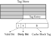
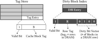
Figure 8.1 compares the conventional tag store with a tag store augmented with a DBI. In the conventional organization (shown in Figure 8.1(a)), each tag entry contains a dirty bit that indicates whether the corresponding block is dirty or not. For example, to indicate that a block B is dirty, the dirty bit of the corresponding tag entry is set.
In contrast, in a cache augmented with a DBI (Figure 8.1(b)), the dirty bits are removed from the main tag store and organized differently in the DBI. The organization of DBI is simple. It consists of multiple entries. Each entry corresponds to some row in DRAM—identified using a row tag present in each entry. Each DBI entry contains a dirty bit vector that indicates if each block in the corresponding DRAM row is dirty or not.
DBI Semantics. A block in the cache is dirty if and only if the DBI contains a valid entry for the DRAM row that contains the block and the bit corresponding to the block in the bit vector of that DBI entry is set. For example, assuming that block B is the second block of DRAM row R, to indicate that block B is dirty, the DBI contains a valid entry for DRAM row R, with the second bit of the corresponding bit vector set.
Note that the key difference between the DBI and the conventional tag store is the logical organization of the dirty bit information. While some processors store the dirty bit information in a separate physical structure, the logical organization of the dirty bit information is same as the main tag store.
8.2.2 DBI Operation
Figure 8.2 pictorially describes the operation of a cache augmented with a DBI. The focus of this work is on the on-chip last-level cache (LLC). Therefore, for ease of explanation, we assume that the cache does not receive any sub-block writes and any dirty block in the cache is a result of a writeback generated by the previous level of cache.111Sub-block writes typically occur in the primary L1 cache where writes are at a word-granularity, or at a cache which uses a larger block size than the previous level of cache. The DBI operation described in this paper can be easily extended to caches with sub-block writes. There are four possible operations, which we describe in detail below.
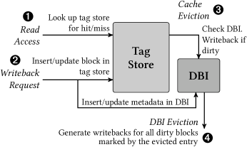
Read Access to the Cache
The addition of DBI does not change the path of a read access in any way. On a read access, the cache simply looks up the block in the tag store and returns the data on a cache hit. Otherwise, it forwards the access to the memory controller.
Writeback Request to the Cache
In a system with multiple levels of on-chip cache, the LLC will receive a writeback request when a dirty block is evicted from the previous level of cache. Upon receiving such a writeback request, the cache performs two actions (as shown in Figure 8.2). First, it inserts the block into the cache if it is not already present. This may result in a cache block eviction (discussed in Section 8.2.2). If the block is already present in the cache, the cache just updates the data store (not shown in the figure) with the new data. Second, the cache updates the DBI to indicate that the written-back block is dirty. If the DBI already has an entry for the DRAM row that contains the block, the cache simply sets the bit corresponding to the block in that DBI entry. Otherwise, the cache inserts a new entry into the DBI for the DRAM row containing the block and with the bit corresponding to the block set. Inserting a new entry into the DBI may require an existing DBI entry to be evicted. Section 8.2.2 discusses how the cache handles such a DBI eviction.
Cache Eviction
When a block is evicted from the cache, it has to be written back to main memory if it is dirty. Upon a cache block eviction, the cache consults the DBI to determine if the block is dirty. If so, it first generates a writeback request for the block and sends it to the memory controller. It then updates the DBI to indicate that the block is no longer dirty—done by simply resetting the bit corresponding to the block in the bit vector of the DBI entry. If the evicted block is the last dirty block in the corresponding DBI entry, the cache invalidates the DBI entry so that the entry can be used to store the dirty block information of some other DRAM row.
DBI Eviction
The last operation in a cache augmented with a DBI is a DBI eviction. Similar to the cache, since the DBI has limited space, it can only track the dirty block information for a limited number of DRAM rows. As a result, inserting a new DBI entry (on a writeback request, discussed in Section 8.2.2) may require evicting an existing DBI entry. We call this event a DBI eviction. The DBI entry to be evicted is decided by the DBI replacement policy (discussed in Section 8.3.3). When an entry is evicted from the DBI, all the blocks indicated as dirty by the entry should be written back to main memory. This is because, once the entry is evicted, the DBI can no longer maintain the dirty status of those blocks. Therefore, not writing them back to memory will likely lead to incorrect execution, as the version of those blocks in memory is stale. Although a DBI eviction may require evicting many dirty blocks, with a small buffer to keep track of the evicted DBI entry (until all of its blocks are written back to memory), the DBI eviction can be interleaved with other demand requests. Note that on a DBI eviction, the corresponding cache blocks need not be evicted—they only need to be transitioned from the dirty state to clean state.
8.2.3 Cache Coherence Protocols
Many cache coherence protocols implicitly store the dirty status of cache blocks in the cache coherence states. For example, in the MESI protocol [168], the M (modified) state indicates that the block is dirty. In the improved MOESI protocol [219], both M (modified) and O (Owner) states indicate that the block is dirty. To adapt such protocols to work with DBI, we propose to split the cache coherence states into multiple pairs—each pair containing a state that indicates the block is dirty and the non-dirty version of the same state. For example, we split the MOESI protocol into three parts: (M, E), (O, S) and (I). We can use a single bit to then distinguish between the two states in each pair. This bit will be stored in the DBI.
8.3 DBI Design Choices
The DBI design space can be defined using three key parameters: 1) DBI size, 2) DBI granularity and 3) DBI replacement policy.222DBI is also a set-associative structure and has a fixed associativity. However, we do not discuss the DBI associativity in detail as its trade-offs are similar to any other set-associative structure. These parameters determine the effectiveness of the three optimizations discussed in the previous section. We now discuss these parameters and their trade-offs in detail.
8.3.1 DBI Size
The DBI size refers to the cumulative number of blocks tracked by all the entries in the DBI. For ease of analysis across systems with different cache sizes, we represent the DBI size as the ratio of the cumulative number of blocks tracked by the DBI and the number of blocks tracked by the cache tag store. We denote this ratio using . For example, for a 1MB cache with a 64B block size (16k blocks), a DBI of size enables the DBI to track 8k blocks.
The DBI size presents a trade-off between the size of write working set (set of frequently written blocks) that can be captured by the DBI, and the area, latency, and power cost of the DBI. A large DBI has two benefits: 1) it can track a larger write working set, thereby reducing the writeback bandwidth demand, and 2) it gives more time for a DBI entry to accumulate writebacks to a DRAM row, thereby better exploiting the AWB optimization. However, a large DBI comes at a higher area, latency and power cost. On the other hand, a smaller DBI incurs lower area, latency and power cost. This has two benefits: 1) lower latency in the critical path for the CLB optimization and 2) ECC storage for fewer dirty blocks. However, a small DBI limits the number of dirty blocks in the cache and thus, result in premature DBI evictions, reducing the potential to generate aggressive writebacks. It can also potentially lead to thrashing if the write working set is significantly larger than the number of blocks tracked by the small DBI.
8.3.2 DBI Granularity
The DBI granularity refers to the number of blocks tracked by a single DBI entry. Although our discussion in Section 8.2 suggests that this is same as the number of blocks in each DRAM row, we can design the DBI to track fewer blocks in each entry. For example, for a system with DRAM row of size 8KB and cache block of size 64B, a natural choice for the DBI granularity is 8KB/64B = 128. Instead, we can design a DBI entry to track only 64 blocks, i.e. one half of a DRAM row.
The DBI granularity presents another trade-off between the amount of locality that can be extracted during the writeback phase (using the AWB optimization) and the size of write working set that can be captured using the DBI. A large granularity leads to better potential for exploiting the AWB optimization. However, if writes have low spatial locality, a large granularity will result in inefficient use of the DBI space, potentially leading to write working set thrashing.
8.3.3 DBI Replacement Policy
The DBI replacement policy determines which entry is evicted on a DBI eviction (Section 8.2.2). A DBI eviction only writes back the dirty blocks of the corresponding DRAM row to main memory, and does not evict the blocks themselves from the cache. Therefore, a DBI eviction does not affect the latency of future read requests for the corresponding blocks. However, if the previous cache level generates a writeback request for a block written back due to a DBI eviction, the block will have to be written back again, leading to an additional write to main memory. Therefore, the goal of the DBI replacement policy is to ensure that blocks are not prematurely written back to main memory.
The ideal policy is to evict the entry that has a writeback request farthest into the future. However, similar to Belady’s optimal replacement policy [32], this ideal policy is impractical to implement in real systems. We evaluated five practical replacement policies for DBI: 1) Least Recently Written (LRW)—similar to the LRU policy for caches, 2) LRW with Bimodal Insertion Policy [176], 3) Rewrite-interval prediction policy—similar to the RRIP policy for caches [106], 4) Max-Dirty—entry with the maximum number of dirty blocks, 5) Min-Dirty—entry with the minimum number of dirty blocks. We find that the LRW policy works comparably or better than the other policies.
8.4 Bulk Data Coherence with DBI
As mentioned in Section 8.2, we conceived of DBI to primarily improve the performance of the DRAM-Aware Writeback optimization. However, we identified several other potential use cases for DBI, and quantitatively evaluated three such optimizations (including DRAM-aware Writeback). Since these optimizations are not directly related to this thesis, we only provide a brief summary of the evaluated optimizations and the results in Section 8.5. We direct the reader to our paper published in ISCA 2014 [190] for more details. In this section, we describe how DBI can be used to improve the performance of certain cache coherence protocol operations, specifically flushing bulk data.
8.4.1 Checking If a Block is Dirty
As described in Section 8.2, in the cache organization used in existing systems, the cache needs to perform a full tag store lookup to check if a block is dirty. Due to the large size and associativity of the last-level cache, the latency of this lookup is typically several processor cycles. In contrast, in a cache augmented with DBI, the cache only needs to perform a single DBI lookup to check if a block is dirty. Based on our evaluations, even with just 64 DBI entries (in comparison to 16384 entries in the main tag store), the cache with DBI outperforms the conventional cache organization. As a result, checking if a block is dirty is significantly cheaper with the DBI organization.
This fast lookup for the dirty bit information can already make many coherence protocol operations in multi-socket systems more efficient. Specifically, when a processor wants to read a cache line, it has to first check if any of the other processors contain a dirty version of the cache line. With the DBI, this operation is more efficient than in existing systems. However, the major benefit of DBI is in accelerating bulk data flushing.
8.4.2 Accelerating Bulk Data Flushing
In many scenarios, the memory controller must check if a set of blocks belonging to a region is dirty in the on-chip cache. For instance, in Direct Memory Access, the memory controller may send data to an I/O device by directly reading the data from memory. Since these operations typically happen in bulk, the memory controller may have to get all cache lines in an entire page (for example) that are dirty in the on-chip cache. In fact, all the DRAM-related mechanisms described in the previous three chapters of this thesis require an efficient implementation of this primitive.
With a cache augmented DBI, this primitive can be implemented with just a single DBI lookup. When the controller wants to extract all the dirty cache lines of a region, it looks up the DBI with the DBI tag for the corresponding region, and extracts the dirty bit vector, which indicates which blocks within the region are dirty in the cache. If the size of the region is larger than the segment tracked by each DBI entry, the memory controller must perform multiple lookups. However, with the DBI, 1) the memory controller has to perform 64X or 128X (depending on the DBI granularity) fewer lookups compared to conventional cache organization, 2) each DBI lookup is cheaper than a tag store lookup, and 3) the cache can lookup and flush only blocks that are actually dirty. With these benefits, DBI can perform flush data in bulk faster than existing organizations.
8.5 Summary of Optimizations and Evaluations
In this section, we provide a brief summary of the optimizations enabled by DBI and the corresponding evaluation. We refer the reader to our ISCA paper [190] for more details. We specifically evaluate the following three optimizations in detail: 1) DRAM-aware writeback, 2) cache lookup bypass, and 3) heterogeneous ECC.
8.5.1 Optimizations
Efficient DRAM-aware Writeback
This is the optimization we described briefly in Section 8.2. The key idea is to cluster writebacks to dirty blocks of individual DRAM rows with the goal of maximizing the write row buffer hit rate. Implementing this optimization with DBI is straightforward. When a block is evicted from the cache, the DBI tells the cache whether the block is dirty or not. In addition, the bit vector in the corresponding DBI entry also tells the cache the list of all other dirty blocks in the corresponding DRAM row (assuming that each region in the DBI corresponds to a DRAM row). The cache can then selectively lookup only those dirty blocks and write them back to main memory. This is significantly more efficient than the implementation with the block-oriented organization. The best case for DBI is when no other block from the corresponding DRAM row is dirty. In this case, current implementations will have to look up every block in the DRAM row unnecessarily, whereas DBI will perform zero additional lookups.
Bypassing Cache Lookups
The idea behind this optimization is simple: If an access is likely to miss in the cache, then we can avoid the tag lookup for the access, reducing both latency and energy consumption of the access. In this optimization, the cache is augmented with a miss predictor which can efficiently predict if an access will hit or miss in the cache. If an access is predicted to miss, then the request is directly sent to main memory. The main challenge with this optimization is that an access to a dirty block should not be bypassed. This restricts the range of miss predictors as the predictor cannot falsely predict that an access will miss in the cache [149]. Fortunately, with the DBI, when an access is predicted to miss, the cache can first consult the DBI to ensure that the block is not dirty before bypassing the tag lookup. As a result, DBI enables very aggressive miss predictors (e.g., bypass all accesses of an application [115]).
Reducing ECC Overhead
The final optimization is again based on a simple idea: clean blocks need only error detection; only dirty blocks need strong error correction. Several prior works have propose mechanisms to exploit this observation to reduce the ECC overhead. However, they require complex mechanisms to handle the case when an error is detected on a dirty block (e.g., [241]). In our proposed organization, since DBI tracks dirty blocks, it is sufficient to store ECC only for the blocks tracked by DBI. With the previously discussed optimizations, we find that the DBI can get away with tracking far fewer blocks than the main cache. As a result, DBI can seamlessly reduce the ECC area overhead (8% reduction in overall cache area).
8.5.2 Summary of Results
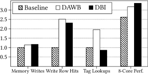
We refer the reader to our paper for full details on our methodology. Figure 8.3 briefly summarizes the comparison between DBI (with the first two optimizations, DRAM-aware writeback and cache lookup bypass) and the best previous mechanism, DRAM-aware writeback [133] (DAWB). As a result of proactively writing back blocks to main memory, both mechanisms increase the number of memory writes. However, for a small increase in the number of writes, both mechanisms significantly improve the write row hit rate, and hence also performance compared to the baseline. However, the key difference between DAWB and DBI is that DAWB almost doubles the number of tag lookups, whereas with both optimizations, DBI actually reduces the number of tag lookups by 14% compared to the baseline. As a result, DBI improves performance by 6% compared to DAWB (31% over baseline) across 120 workloads in an 8-core system with 16MB shared cache.
8.6 Summary
In this chapter, we introduced the Dirty-Block Index (DBI), a structure that aids the cache in efficiently responding to queries regarding dirty blocks. Specifically, DBI can quickly list all dirty blocks that belong to a contiguous region and, in general, check if a block is dirty more efficiently than existing cache organization. To achieve this, our mechanism removes the dirty bits from the on-chip tag store and organizes them at a large region (e.g., DRAM row) granularity in the DBI. DBI can be used to accelerate the coherence protocol that ensures the coherence of data between the on-chip caches and main memory in our in-DRAM mechanisms. We described three other concrete use cases for the DBI that can improve the performance and energy-efficiency of the memory subsystem in general, and reduce the ECC overhead for on-chip caches. This approach is an effective way of enabling several other optimizations at different levels of caches by organizing the DBI to cater to the write patterns of each cache level. We believe this approach can be extended to more efficiently organize other metadata in caches (e.g., cache coherence states), enabling more optimizations to improve performance and power-efficiency.
Chapter 9 Conclusions & Future Work
In modern systems, different resources of the memory subsystem store and access data at different granularities. Specifically, virtual memory manages main memory capacity at a (large) page granularity; the off-chip memory interface access data from memory at a cache line granularity; on-chip caches typically store and access data at a cache line granularity; applications typically access data at a (small) word granularity. We observe that this mismatch in granularities results in significant inefficiency for many memory operations. In Chapter 2, we demonstrate this inefficiency using two example operations: copy-on-write and non-unit strided access.
9.1 Contributions of This Dissertation
In this dissertation, we propose five distinct mechanisms to address the inefficiency problem at various structures. First, we observe that page-granularity management of main memory capacity can result in significant inefficiency in implementing many memory management techniques. In Chapter 3, we describe page overlays, a new framework which augments the existing virtual memory framework with a structure called overlays. In short, an overlay of a virtual page tracks a newer version of a subset of segments from within the page. We show that this simple framework is very powerful and enables many applications. We quantitatively evaluate page overlays with two mechanisms: overlay-on-write, a more efficient version of the widely-used copy-on-write technique, and an efficient hardware-based representation for sparse data structures.
Second, we show that the internal organization and operation of a DRAM chip can be used to transfer data quickly and efficiently from one location to another. Exploiting this observation, in Chapter 5, we describe RowClone, a mechanism to perform bulk copy and initialization operations completely inside DRAM. RowClone reduces the latency and energy of performing a bulk copy operation by 11X and 74X, respectively, compared to commodity DRAM interface. Our evaluations show that this reduction significantly improves the performance of copy and initialization intensive applications.
Third, we show that the analog operation of DRAM and the inverters present in the sense amplifier can be used to perform bitwise logical operations completely inside DRAM. In Chapter 6, we describe Buddy RAM, a mechanism to perform bulk bitwise logical operations using DRAM. Buddy improves the throughput of various bitwise logical operations by between 3.8X (for bitwise XOR) and 10.1X (for bitwise NOT) compared to a multi-core CPU, and reduces the energy consumption of the respective operations by 25.1X and 59.5X. We demonstrate the benefits of Buddy by using it to improve the performance of set operations and in-memory bitmap indices.
Fourth, we show that the multi-chip module organization of off-chip memory can be used to efficiently gather or scatter data with strided access patterns. In Chapter 7, we describe Gather-Scatter DRAM (GS-DRAM), a mechanism that achieves near-ideal bandwidth utilization for any power-of-2 strided access pattern. We implement an in-memory database on top of GS-DRAM and show that GS-DRAM gets the best of both a row store layout and column store layout on a transactions workload, analytics workload, and a hybrid transactions and analytics workload.
Finally, in Chapter 8, we introduce the Dirty-Block Index, a mechanism to improve the efficiency of the coherence protocol that ensures the coherence of data across the on-chip caches and main memory. DBI efficiently tracks spatially-collocated dirty blocks, and has several applications in addition to more efficient data coherence, e.g., efficient memory writeback, efficient cache lookup bypass, and reducing cache ECC overhead.
9.2 Future Research Directions
This dissertation opens up several avenues for research. In this section, we describe six specific directions in which the ideas and approaches proposed in this thesis can be extended to other problems to improve the performance and efficiency of various systems.
9.2.1 Extending Overlays to Superpages
In Chapter 3, we described and evaluated the benefits of our page overlays mechanism for regular 4KB pages. We believe that our mechanism can be easily extended to superpages, which are predominantly used by many modern operating systems. The primary benefit of using superpages is to increase TLB reach and thereby reduce overall TLB misses. However, we observe that superpages are ineffective for reducing memory redundancy.
To understand this, let us consider the scenario when multiple virtual superpages are mapped to the same physical page in the copy-on-write mode (as a result of cloning a process or a virtual machine). In this state, if any of the virtual superpages receives a write, the operating system has two options: 1) allocate a new superpage and copy all the data from the old superpage to the newly allocated superpage, and 2) break the virtual superpage that received the write and copy only the 4KB page that was modified. While the former approach enables low TLB misses, it results in significant redundancy in memory. On the other hand, while the latter approach reduces memory redundancy, it sacrifices the TLB miss reduction benefits of using a super page.
Extending overlays to superpages will allow the operating systems to track small modifications to a superpage using an overlay. As a result, our approach can potentially get both the TLB miss reduction benefits of having a superpage mapping and the memory redundancy benefits by using the overlays to track modifications.
9.2.2 Using Overlays to Store and Operate on Metadata
In the page overlays mechanism described in Chapter 3, we used overlays to track a newer version of data for each virtual page. Alternatively, each overlay can be used to store metadata for the corresponding virtual page instead of a newer version of the data. Since the hardware is aware of overlays, it can provide an efficient abstraction to the software for maintaining metadata for various applications, e.g., memory error checking, security. We believe using overlays to maintain metadata can also enable new and efficient computation models, e.g., update-triggered computation.
9.2.3 Efficiently Performing Reduction and Shift Operations in DRAM
In Chapters 5 and 6, we described mechanisms to perform bulk copy, initialization, and bitwise logical operations completely inside DRAM. These set of operations will enable the memory controller to perform some primitive level of bitwise computation completely inside DRAM. However, these mechanisms lack support for two operations that are required by many applications: 1) data reduction, and 2) bit shifting.
First, RowClone and Buddy operate at a row-buffer granularity. As a result, to perform any kind of reduction within the row buffer (e.g., bit counting, accumulation), the data must be read into the processor. Providing support for such operations in DRAM will further reduce the amount of bandwidth consumed by many queries. While GS-DRAM (Chapter 7) enables a simple form of reduction (i.e., selection), further research is required to enable support for more complex reduction operations.
Second, many applications, such as encryption algorithms in cryptography, heavily rely on bit shifting operations. Enabling support for bit shifting in DRAM can greatly improve the performance of such algorithms. However, there are two main challenges in enabling support for bit shifting in DRAM. First, we need to design a low-cost DRAM substrate that can support moving data between multiple bitlines. Given the rigid design of modern DRAM chips, this can be difficult and tricky, especially when we need support for multiple shifts. Second, the physical address space is heavily interleaved on the DRAM hierarchy [143, 120]). As a result, bits that are adjacent in the physical address space may not map to adjacent bitlines in DRAM, adding complexity to the data mapping mechanism.
9.2.4 Designing Efficient ECC Mechanisms for Buddy/GS-DRAM
Most server memory modules use error correction codes (ECC) to protect their data. While RowClone works with such ECC schemes without any changes, Buddy (Chapter 6) and GS-DRAM (Chapter 7) can break existing ECC mechanisms. Designing low-cost ECC mechanisms that work with Buddy and GS-DRAM will be critical to their adoption. While Section 7.4 already describes a simple way of extending GS-DRAM to support ECC, such a mechanism will work only with a simple SECDED ECC mechanism. Further research is required to design mechanisms that will 1) enable GS-DRAM with stronger ECC schemes and 2) provide low-cost ECC support for Buddy.
9.2.5 Extending In-Memory Computation to Non-Volatile Memories
Recently, many new non-volatile memory technologies (e.g., phase change memory [132, 177, 237, 254], STT MRAM [51, 121, 251, 128]) have emerged as a scalable alternative to DRAM. In fact, Intel has recently announced a real product [99] based on a non-volatile memory technology. These new technologies are expected to have better scalability properties than DRAM. In future systems, while we expect DRAM to still play some role, bulk of the data may actually be stored in non-volatile memory. This raises a natural question: can we extend our in-memory data movement and computation techniques to the new non-volatile memory technologies? Answering this question requires a thorough understanding of these new technologies (i.e., how they store data at the lowest level, what is the architecture used to package them, etc.).
9.2.6 Extending DBI to Other Caches and Metadata
In Chapter 8, we described the Dirty-Block Index (DBI), which reorganizes the way dirty blocks are tracked (i.e., the dirty bits are stored) to enable the cache to efficiently respond to queries related to dirty blocks. In addition to the dirty bit, the on-chip cache stores several other pieces of metadata, e.g., valid bit, coherence state, and ECC, for each cache block. In existing caches, all this information is stored in the tag entry of the corresponding block. As a result, a query for any metadata requires a full tag store lookup. Similar to the dirty bits, these other pieces of metadata can potentially be organized to suit the queries for each one, rather than organizing them the way the tag stores do it today.
9.3 Summary
In this dissertation, we highlighted the inefficiency problem that results from the different granularities at which different memory resources (e.g., caches, DRAM) are managed and accessed. We presented techniques that bridge this granularity mismatch for several important memory operations: a new virtual memory framework that enables memory capacity management at sub-page granularity (Page Overlays), techniques to use DRAM to do more than just store data (RowClone, Buddy RAM, and Gather-Scatter DRAM), and a simple hardware structure for more efficient management of dirty blocks (Dirty-Block Index). As we discussed in Section 9.2, these works open up many avenues for new research that can result in techniques to enable even higher efficiency.
Other Works of the Author
During the course of my Ph.D., I had the opportunity to collaborate many of my fellow graduate students. These projects were not only helpful in keeping my morale up, especially during the initial years of my Ph.D., but also helped me in learning about DRAM (an important aspect of this dissertation). In this chapter, I would like to acknowledge these projects and also my early works on caching, which kick started my Ph.D.
My interest in DRAM was triggered my work on subarray-level parallelism (SALP) [125] in collaboration with Yoongu Kim. Since then, I have contributed to a number of projects on low-latency DRAM architectures with Donghyuk Lee (Tiered-Latency DRAM [137] and Adaptive-Latency DRAM [136]), and Hasan Hassan (Charge Cache [89]). These works focus on improving DRAM performance by either increasing parallelism or lowering latency through low-cost modifications to the DRAM interface and/or microarchitecture.
In collaboration with Gennady Pekhimenko, I have worked on designing techniques to support data compression in a modern memory hierarchy. Two contributions have resulted from this work: 1) Base-Delta Immediate Compression [173], an effective data compression algorithm for on-chip caches, and 2) Linearly Compressed Pages [172], a low-cost framework for storing compressed data in main memory.
In collaboration with Lavanya Subramanian, I have worked on techniques to quantify and mitigate slowdown in a multi-core system running multi-programmed workloads. This line of work started with MISE [215], a mechanism to estimate slowdown induced by contention for memory bandwidth. Later, we extended this with Application Slowdown Model [216], mechanism that accounts for contention for on-chip cache capacity. Finally, we propose the Blacklisting Memory Scheduler [213, 214], a simple memory scheduling algorithm to achieve high performance and fairness with low complexity.
Finally, in the early years of my Ph.D., I have worked on techniques to improve on-chip cache utilization using 1) the Evicted-Address Filter [194], an improved cache insertion policy to address pollution and thrashing, and 2) ICP [196], a mechanism that better integrates caching policy for prefetched blocks. We have released memsim [16], the simulator that we developed as part of the EAF work. The simulator code can be found in github (github.com/CMU-SAFARI/memsim). memsim has since been used for many works [196, 173, 190, 172].
References
- [1] Belly card engineering. https://tech.bellycard.com/.
- [2] bitmapist: Powerful realtime analytics with Redis 2.6’s bitmaps and Python. https://github.com/Doist/bitmapist.
- [3] Bochs IA-32 emulator project. http://bochs.sourceforge.net/.
- [4] C++ containers libary, std::set. http://en.cppreference.com/w/cpp/container/set.
- [5] FastBit: An Efficient Compressed Bitmap Index Technology. https://sdm.lbl.gov/fastbit/.
- [6] High Bandwidth Memory DRAM. http://www.jedec.org/standards-documents/docs/jesd235.
- [7] Intel 64 and IA-32 Architectures Software Developer’s Manual. http://download.intel.com/design/processor/manuals/253665.pdf, Vol. 1, Chap. 3.7.
- [8] Memcached: A high performance, distributed memory object caching system. http://memcached.org.
- [9] MySQL: An open source database. http://www.mysql.com.
- [10] Redis - bitmaps. http://redis.io/topics/data-types-intro#bitmaps.
- [11] rlite: A Self-contained, Serverless, Zero-configuration, Transactional Redis-compatible Database Engine. https://github.com/seppo0010/rlite.
- [12] Spool. http://www.getspool.com/.
- [13] Wind River Simics full system simulation. http://www.windriver.com/products/simics/.
- [14] The NON-VON Database Machine: An Overview. http://hdl.handle.net/10022/AC:P:11530., 1981.
- [15] Alpha 21264 Microprocessor Hardware Reference Manual. http://h18000.www1.hp.com/cpq-alphaserver/technology/literature/21264hrm.pdf, 1999.
- [16] Memsim. http://safari.ece.cmu.edu/tools.html, 2012.
- [17] Hybrid Transaction/Analytical Processing Will Foster Opportunities for Dramatic Business Innovation. https://www.gartner.com/doc/2657815/hybrid- transactionanalytical-processing-foster -opportunities, 2014.
- [18] J. H. Ahn, J. Leverich, R. Schreiber, and N. P. Jouppi. Multicore DIMM: An Energy Efficient Memory Module with Independently Controlled DRAMs. IEEE CAL, January 2009.
- [19] Jung Ho Ahn, Norman P. Jouppi, Christos Kozyrakis, Jacob Leverich, and Robert S. Schreiber. Future Scaling of Processor-memory Interfaces. In SC, 2009.
- [20] Junwhan Ahn, Sungpack Hong, Sungjoo Yoo, Onur Mutlu, and Kiyoung Choi. A Scalable Processing-in-memory Accelerator for Parallel Graph Processing. In Proceedings of the 42nd Annual International Symposium on Computer Architecture, ISCA ’15, pages 105–117, New York, NY, USA, 2015. ACM.
- [21] Junwhan Ahn, Sungjoo Yoo, Onur Mutlu, and Kiyoung Choi. PIM-enabled Instructions: A Low-overhead, Locality-aware Processing-in-memory Architecture. In Proceedings of the 42nd Annual International Symposium on Computer Architecture, ISCA ’15, pages 336–348, New York, NY, USA, 2015. ACM.
- [22] A. Akerib, O. AGAM, E. Ehrman, and M. Meyassed. Using storage cells to perform computation, December 2014. US Patent 8,908,465.
- [23] Avidan Akerib and Eli Ehrman. In-memory Computational Device, Patent No. 20150146491, May 2015.
- [24] Berkin Akin, Franz Franchetti, and James C. Hoe. Data Reorganization in Memory Using 3D-stacked DRAM. In Proceedings of the 42nd Annual International Symposium on Computer Architecture, ISCA ’15, pages 131–143, New York, NY, USA, 2015. ACM.
- [25] C. Scott Ananian, Krste Asanovic, Bradley C. Kuszmaul, Charles E. Leiserson, and Sean Lie. Unbounded Transactional Memory. In Proceedings of the 11th International Symposium on High-Performance Computer Architecture, HPCA ’05, pages 316–327, Washington, DC, USA, 2005. IEEE Computer Society.
- [26] Rachata Ausavarungnirun, Kevin Kai-Wei Chang, Lavanya Subramanian, Gabriel H. Loh, and Onur Mutlu. Staged Memory Scheduling: Achieving High Performance and Scalability in Heterogeneous Systems. In Proceedings of the 39th Annual International Symposium on Computer Architecture, ISCA ’12, pages 416–427, Washington, DC, USA, 2012. IEEE Computer Society.
- [27] Rachata Ausavarungnirun, Saugata Ghose, Onur Kayiran, Gavriel H. Loh, Chita R. Das, Mahmut T. Kandemir, and Onur Mutlu. Exploiting Inter-Warp Heterogeneity to Improve GPGPU Performance. In Proceedings of the 2015 International Conference on Parallel Architecture and Compilation (PACT), PACT ’15, 2015.
- [28] Oreoluwatomiwa O. Babarinsa and Stratos Idreos. JAFAR: Near-Data Processing for Databases. In Proceedings of the 2015 ACM SIGMOD International Conference on Management of Data, SIGMOD ’15, pages 2069–2070, New York, NY, USA, 2015. ACM.
- [29] Seungjae Baek, Sangyeun Cho, and Rami Melhem. Refresh Now and Then. IEEE Trans. Comput., 63(12):3114–3126, December 2014.
- [30] Jean-Loup Baer and Tien-Fu Chen. Effective Hardware-Based Data Prefetching for High-Performance Processors. IEEE TC, 1995.
- [31] Arkaprava Basu, Jayneel Gandhi, Jichuan Chang, Mark D. Hill, and Michael M. Swift. Efficient Virtual Memory for Big Memory Servers. In Proceedings of the 40th Annual International Symposium on Computer Architecture, ISCA ’13, pages 237–248, New York, NY, USA, 2013. ACM.
- [32] L. A. Belady. A study of replacement algorithms for a virtual-storage computer. IBM Systems Journal, 5(2):78 –101, 1966.
- [33] John Bent, Garth Gibson, Gary Grider, Ben McClelland, Paul Nowoczynski, James Nunez, Milo Polte, and Meghan Wingate. PLFS: A Checkpoint Filesystem for Parallel Applications. In Proceedings of the Conference on High Performance Computing Networking, Storage and Analysis, SC ’09, pages 21:1–21:12, New York, NY, USA, 2009. ACM.
- [34] Nathan Binkert, Bradford Beckmann, Gabriel Black, Steven K. Reinhardt, Ali Saidi, Arkaprava Basu, Joel Hestness, Derek R. Hower, Tushar Krishna, Somayeh Sardashti, Rathijit Sen, Korey Sewell, Muhammad Shoaib, Nilay Vaish, Mark D. Hill, and David A. Wood. The gem5 simulator. SIGARCH Comput. Archit. News, 39(2):1–7, August 2011.
- [35] D. L. Black, R. F. Rashid, D. B. Golub, and C. R. Hill. Translation Lookaside Buffer Consistency: A Software Approach. In Proceedings of the Third International Conference on Architectural Support for Programming Languages and Operating Systems, ASPLOS III, pages 113–122, New York, NY, USA, 1989. ACM.
- [36] D. P. Bovet and M. Cesati. Understanding the Linux Kernel, page 388. O’Reilly Media, 2005.
- [37] Oscar Boykin, Sam Ritchie, Ian O’Connell, and Jimmy Lin. Summingbird: A framework for integrating batch and online mapreduce computations. Proc. VLDB Endow., 7(13):1441–1451, August 2014.
- [38] T. M. Brewer. Instruction Set Innovations for the Convey HC-1 Computer. IEEE Micro, 30(2):70–79, March 2010.
- [39] J. Carter, W. Hsieh, L. Stoller, M. Swanson, L. Zhang, E. Brunvand, A. Davis, C.-C. Kuo, R. Kuramkote, M. Parker, L. Schaelicke, and T. Tateyama. Impulse: Building a Smarter Memory Controller. In HPCA, 1999.
- [40] Michel Cekleov and Michel Dubois. Virtual-address caches part 1: Problems and solutions in uniprocessors. IEEE Micro, 17(5):64–71, September 1997.
- [41] Chee-Yong Chan and Yannis E. Ioannidis. Bitmap index design and evaluation. In Proceedings of the 1998 ACM SIGMOD International Conference on Management of Data, SIGMOD ’98, pages 355–366, New York, NY, USA, 1998. ACM.
- [42] K. Chandrasekar, B. Akesson, and K. Goossens. Improved Power Modeling of DDR SDRAMs. In DSD, 2011.
- [43] K. Chandrasekar, C. Weis, Y. Li, S. Goossens, M. Jung, O. Naji, B. Akesson, N. Wehn, and K. Goossens. DRAMPower: Open-source DRAM Power & Energy Estimation Tool. http://www.drampower.info.
- [44] Fay Chang and Garth A. Gibson. Automatic I/O Hint Generation Through Speculative Execution. In Proceedings of the Third Symposium on Operating Systems Design and Implementation, OSDI ’99, pages 1–14, Berkeley, CA, USA, 1999. USENIX Association.
- [45] Kevin K. Chang, Abhijith Kashyap, Hasan Hassan, Saugata Ghose, Kevin Hsieh, Donghyuk Lee, Tianshi Li, Gennady Pekhimenko, Samira Khan, and Onur Mutlu. Understanding Latency Variation in Modern DRAM Chips: Experimental Characterization, Analysis, and Optimization. In Sigmetrics, 2016.
- [46] Kevin K Chang, Prashant J Nair, Donghyuk Lee, Saugata Ghose, Moinuddin K Qureshi, and Onur Mutlu. Low-Cost Inter-Linked Subarrays (LISA): Enabling Fast Inter-Subarray Data Movement in DRAM. In HPCA, 2016.
- [47] Kevin Kai-Wei Chang, Donghyuk Lee, Zeshan Chishti, Alaa R Alameldeen, Chris Wilkerson, Yoongu Kim, and Onur Mutlu. Improving DRAM performance by parallelizing refreshes with accesses. In 2014 IEEE 20th International Symposium on High Performance Computer Architecture (HPCA), pages 356–367. IEEE, 2014.
- [48] David Cheriton, Amin Firoozshahian, Alex Solomatnikov, John P. Stevenson, and Omid Azizi. HICAMP: Architectural Support for Efficient Concurrency-safe Shared Structured Data Access. In ASPLOS, pages 287–300, New York, NY, USA, 2012. ACM.
- [49] Jungwhan Choi, Wongyu Shin, Jaemin Jang, Jinwoong Suh, Yongkee Kwon, Youngsuk Moon, and Lee-Sup Kim. Multiple Clone Row DRAM: A Low Latency and Area Optimized DRAM. In Proceedings of the 42nd Annual International Symposium on Computer Architecture, ISCA ’15, pages 223–234, New York, NY, USA, 2015. ACM.
- [50] Jim Chow, Ben Pfaff, Tal Garfinkel, and Mendel Rosenblum. Shredding Your Garbage: Reducing Data Lifetime Through Secure Deallocation. In Proceedings of the 14th Conference on USENIX Security Symposium - Volume 14, SSYM’05, pages 22–22, Berkeley, CA, USA, 2005. USENIX Association.
- [51] K. C. Chun, H. Zhao, J. D. Harms, T. H. Kim, J. P. Wang, and C. H. Kim. A Scaling Roadmap and Performance Evaluation of In-Plane and Perpendicular MTJ Based STT-MRAMs for High-Density Cache Memory. IEEE Journal of Solid-State Circuits, 48(2):598–610, Feb 2013.
- [52] Kypros Constantinides, Onur Mutlu, and Todd Austin. Online Design Bug Detection: RTL Analysis, Flexible Mechanisms, and Evaluation. In Proceedings of the 41st Annual IEEE/ACM International Symposium on Microarchitecture, MICRO 41, pages 282–293, Washington, DC, USA, 2008. IEEE Computer Society.
- [53] Kypros Constantinides, Onur Mutlu, Todd Austin, and Valeria Bertacco. Software-Based Online Detection of Hardware Defects Mechanisms, Architectural Support, and Evaluation. In Proceedings of the 40th Annual IEEE/ACM International Symposium on Microarchitecture, MICRO 40, pages 97–108, Washington, DC, USA, 2007. IEEE Computer Society.
- [54] Intel Corporation. Intel Architecture Instruction Set Extensions Programming Reference, chapter 8. Intel Transactional Synchronization Extensions. Sep 2012.
- [55] Standard Performance Evaluation Corporation. SPEC CPU2006 Benchmark Suite. www.spec.org/cpu2006, 2006.
- [56] W. Dally and B. Towles. Principles and Practices of Interconnection Networks. Morgan Kaufmann Publishers Inc., San Francisco, CA, USA, 2003.
- [57] William Dally. GPU Computing to Exascale and Beyond. http://www.nvidia.com/content/PDF/sc_2010/theater/Dally_SC10.pdf.
- [58] Timothy A. Davis and Yifan Hu. The University of Florida Sparse Matrix Collection. ACM Trans. Math. Softw., 38(1):1:1–1:25, December 2011.
- [59] Demiz Denir, Islam AbdelRahman, Liang He, and Yingsheng Gao. Audience Insights query engine: In-memory integer store for social analytics. https://code.facebook.com/posts/382299771946304/ audience-insights-query-engine-in-memory- integer-store-for-social-analytics-/.
- [60] Peter J. Denning. Virtual Memory. ACM Comput. Surv., 2(3):153–189, September 1970.
- [61] Jeff Draper, Jacqueline Chame, Mary Hall, Craig Steele, Tim Barrett, Jeff LaCoss, John Granacki, Jaewook Shin, Chun Chen, Chang Woo Kang, Ihn Kim, and Gokhan Daglikoca. The Architecture of the DIVA Processing-in-memory Chip. In Proceedings of the 16th International Conference on Supercomputing, ICS ’02, pages 14–25, New York, NY, USA, 2002. ACM.
- [62] Alan M. Dunn, Michael Z. Lee, Suman Jana, Sangman Kim, Mark Silberstein, Yuanzhong Xu, Vitaly Shmatikov, and Emmett Witchel. Eternal sunshine of the spotless machine: Protecting privacy with ephemeral channels. In Proceedings of the 10th USENIX Conference on Operating Systems Design and Implementation, OSDI’12, pages 61–75, Berkeley, CA, USA, 2012. USENIX Association.
- [63] Ifeanyi P. Egwutuoha, David Levy, Bran Selic, and Shiping Chen. A Survey of Fault Tolerance Mechanisms and Checkpoint/Restart Implementations for High Performance Computing Systems. J. Supercomput., 65(3):1302–1326, September 2013.
- [64] S. C. Eisenstat, M. C. Gursky, M. H. Schultz, and A. H. Sherman. Yale Sparse Matrix Package I: The Symmetric Codes. IJNME, 18(8), 1982.
- [65] Magnus Ekman and Per Stenstrom. A Robust Main-Memory Compression Scheme. In ISCA, pages 74–85, Washington, DC, USA, 2005. IEEE Computer Society.
- [66] Duncan Elliott, Michael Stumm, W. Martin Snelgrove, Christian Cojocaru, and Robert McKenzie. Computational RAM: Implementing Processors in Memory. IEEE Des. Test, 16(1):32–41, January 1999.
- [67] Stijn Eyerman and Lieven Eeckhout. System-Level Performance Metrics for Multiprogram Workloads. IEEE Micro, 28(3):42–53, May 2008.
- [68] A. Farmahini-Farahani, J. H. Ahn, K. Morrow, and N. S. Kim. NDA: Near-DRAM acceleration architecture leveraging commodity DRAM devices and standard memory modules. In 2015 IEEE 21st International Symposium on High Performance Computer Architecture (HPCA), pages 283–295, Feb 2015.
- [69] A. Farmahini-Farahani, Jung Ho Ahn, K. Morrow, and Nam Sung Kim. NDA: Near-DRAM acceleration architecture leveraging commodity DRAM devices and standard memory modules. In IEEE 21st International Symposium on High Performance Computer Architecture (HPCA), 2015, pages 283–295, Feb 2015.
- [70] Basilio B. Fraguela, Jose Renau, Paul Feautrier, David Padua, and Josep Torrellas. Programming the FlexRAM Parallel Intelligent Memory System. In Proceedings of the Ninth ACM SIGPLAN Symposium on Principles and Practice of Parallel Programming, PPoPP ’03, pages 49–60, New York, NY, USA, 2003. ACM.
- [71] J. M. Frailong, W. Jalby, and J. Lenfant. XOR-Schemes: A Flexible Data Organization in Parallel Memories. In ICPP, 1985.
- [72] J. W. C. Fu and J. H. Patel. Data Prefetching in Multiprocessor Vector Cache Memories. In ISCA, 1991.
- [73] J. W. C. Fu, J. H. Patel, and B. L. Janssens. Stride Directed Prefetching in Scalar Processors. In MICRO, 1992.
- [74] Mingyu Gao, Grant Ayers, and Christos Kozyrakis. Practical Near-Data Processing for In-Memory Analytics Frameworks. In Proceedings of the 2015 International Conference on Parallel Architecture and Compilation (PACT), PACT ’15, pages 113–124, Washington, DC, USA, 2015. IEEE Computer Society.
- [75] Mingyu Gao and Christos Kozyrakis. HRL: Efficient and Flexible Reconfigurable Logic for Near-Data Processing. In HPCA, 2016.
- [76] Saugata Ghose, Hyodong Lee, and José F. Martínez. Improving memory scheduling via processor-side load criticality information. In Proceedings of the 40th Annual International Symposium on Computer Architecture, ISCA ’13, pages 84–95, New York, NY, USA, 2013. ACM.
- [77] Mrinmoy Ghosh and Hsien-Hsin S. Lee. Smart Refresh: An Enhanced Memory Controller Design for Reducing Energy in Conventional and 3D Die-Stacked DRAMs. In Proceedings of the 40th Annual IEEE/ACM International Symposium on Microarchitecture, MICRO 40, pages 134–145, Washington, DC, USA, 2007. IEEE Computer Society.
- [78] Maya Gokhale, Bill Holmes, and Ken Iobst. Processing in Memory: The Terasys Massively Parallel PIM Array. Computer, 28(4):23–31, April 1995.
- [79] Mel Gorman. Understanding the Linux Virtual Memory Manager, chapter 4, page 57. Prentice Hall, 2004.
- [80] Martin Grund, Jens Krüger, Hasso Plattner, Alexander Zeier, Philippe Cudre-Mauroux, and Samuel Madden. Hyrise: A main memory hybrid storage engine. Proc. VLDB Endow., 4(2):105–116, November 2010.
- [81] Leo J. Guibas and Robert Sedgewick. A Dichromatic Framework for Balanced Trees. In Proceedings of the 19th Annual Symposium on Foundations of Computer Science, SFCS ’78, pages 8–21, Washington, DC, USA, 1978. IEEE Computer Society.
- [82] Q. Guo et al. 3D-Stacked Memory-Side Acceleration: Accelerator and System Design. In WoNDP, 2013.
- [83] Diwaker Gupta, Sangmin Lee, Michael Vrable, Stefan Savage, Alex C. Snoeren, George Varghese, Geoffrey M. Voelker, and Amin Vahdat. Difference Engine: Harnessing Memory Redundancy in Virtual Machines. In OSDI, pages 309–322, Berkeley, CA, USA, 2008. USENIX Association.
- [84] H-Store. Anti-Caching. http://hstore.cs.brown.edu/documentation/deployment/anti-caching/, 2015.
- [85] J. Alex Halderman, Seth D. Schoen, Nadia Heninger, William Clarkson, William Paul, Joseph A. Calandrino, Ariel J. Feldman, Jacob Appelbaum, and Edward W. Felten. Lest We Remember: Cold-boot Attacks on Encryption Keys. Commun. ACM, 52(5):91–98, May 2009.
- [86] Jong-Wook Han, Choon-Sik Park, Dae-Hyun Ryu, and Eun-Soo Kim. Optical image encryption based on XOR operations. Optical Engineering, 38(1):47–54, 1999.
- [87] K. Harrison and Shouhuai Xu. Protecting Cryptographic Keys from Memory Disclosure Attacks. In 37th Annual IEEE/IFIP International Conference on Dependable Systems and Networks, pages 137–143, June 2007.
- [88] Milad Hashemi, Khubaib, Eiman Ebrahimi, Onur Mutlu, and Yale N. Patt. Accelerating Dependent Cache Misses with an Enhanced Memory Controller. In ISCA, 2016.
- [89] Hasan Hassan, Gennady Pekhimenko, Nandita Vijaykumar, Vivek Seshadri, Donghyuk Lee, Oguz Ergin, and Onur Mutlu. ChargeCache: Reducing DRAM Latency by Exploiting Row Access Locality. In HPCA, 2016.
- [90] Syed Minhaj Hassan, Sudhakar Yalamanchili, and Saibal Mukhopadhyay. Near Data Processing: Impact and Optimization of 3D Memory System Architecture on the Uncore. In Proceedings of the 2015 International Symposium on Memory Systems, MEMSYS ’15, pages 11–21, New York, NY, USA, 2015. ACM.
- [91] B. He, N. K. Govindaraju, Q. Luo, and B. Smith. Efficient Gather and Scatter Operations on Graphics Processors. In SC, 2007.
- [92] Maurice Herlihy and J. Eliot B. Moss. Transactional Memory: Architectural Support for Lock-free Data Structures. In Proceedings of the 20th Annual International Symposium on Computer Architecture, ISCA ’93, pages 289–300, New York, NY, USA, 1993. ACM.
- [93] Hideto Hidaka, Yoshio Matsuda, Mikio Asakura, and Kazuyasu Fujishima. The Cache DRAM Architecture: A DRAM with an On-Chip Cache Memory. IEEE Micro, 10(2):14–25, March 1990.
- [94] M. Horiguchi and K. Itoh. Nanoscale Memory Repair. Springer, 2011.
- [95] Kevin Hsieh, Eiman Ebrahimi, Gwangsun Kim, Niladrish Chatterjee, Mike O’Conner, Nandita Vijaykumar, Onur Mutlu, and Stephen W. Keckler. Transparent Offloading and Mapping (TOM): Enabling Programmer-Transparent Near-Data Processing in GPU Systems. In ISCA, 2016.
- [96] IBM Corporation. Enterprise Systems Architecture/390 Principles of Operation, 2001.
- [97] Intel. Architecture Guide: Intel Active Management Technology. https://software.intel.com/en-us/articles/architecture-guide-intel-active-management-technology/.
- [98] Intel. Intel Instruction Set Architecture Extensions. https://software.intel.com/en-us/intel-isa-extensions.
- [99] Intel. Non-Volatile Memory. http://www.intel.com/content/www/us/en/architecture-and-technology/non-volatile-memory.html.
- [100] Intel. Sparse Matrix Storage Formats, Intel Math Kernel Library. https://software.intel.com/en-us/node/471374.
- [101] Intel. Intel 64 and IA-32 Architectures Optimization Reference Manual. April 2012.
- [102] Intel. Intel 64 and IA-32 Architectures Software Developer’s Manual, volume 3A, chapter 11, page 12. April 2012.
- [103] Engin Ipek, Onur Mutlu, José F. Martínez, and Rich Caruana. Self-Optimizing Memory Controllers: A Reinforcement Learning Approach. In Proceedings of the 35th Annual International Symposium on Computer Architecture, ISCA ’08, pages 39–50, Washington, DC, USA, 2008. IEEE Computer Society.
- [104] Ciji Isen and Lizy John. ESKIMO: Energy Savings Using Semantic Knowledge of Inconsequential Memory Occupancy for DRAM Subsystem. In Proceedings of the 42nd Annual IEEE/ACM International Symposium on Microarchitecture, MICRO 42, pages 337–346, New York, NY, USA, 2009. ACM.
- [105] Thomas B. Jablin, Prakash Prabhu, James A. Jablin, Nick P. Johnson, Stephen R. Beard, and David I. August. Automatic CPU-GPU Communication Management and Optimization. In Proceedings of the 32nd ACM SIGPLAN Conference on Programming Language Design and Implementation, PLDI ’11, pages 142–151, New York, NY, USA, 2011. ACM.
- [106] Aamer Jaleel, Kevin B. Theobald, Simon C. Steely, Jr., and Joel Emer. High Performance Cache Replacement Using Re-reference Interval Prediction (RRIP). In Proceedings of the 37th Annual International Symposium on Computer Architecture, ISCA ’10, pages 60–71, New York, NY, USA, 2010. ACM.
- [107] J. Jeddeloh and B. Keeth. Hybrid Memory Cube: New DRAM architecture increases density and performance. In VLSIT, pages 87–88, June 2012.
- [108] JEDEC. DDR3 SDRAM Standard, JESD79-3D. http://www.jedec.org/sites/default/files/docs/JESD79-3D.pdf, 2009.
- [109] JEDEC. Standard No. 21-C. Annex K: Serial Presence Detect (SPD) for DDR3 SDRAM Modules, 2011.
- [110] JEDEC. DDR3 SDRAM, JESD79-3F, 2012.
- [111] JEDEC. DDR4 SDRAM Standard. http://www.jedec.org/standards-documents/docs/jesd79-4a, 2013.
- [112] Lei Jiang, Youtao Zhang, and Jun Yang. Mitigating Write Disturbance in Super-Dense Phase Change Memories. In DSN, pages 216–227, Washington, DC, USA, 2014. IEEE Computer Society.
- [113] Xiaowei Jiang, Yan Solihin, Li Zhao, and Ravishankar Iyer. Architecture Support for Improving Bulk Memory Copying and Initialization Performance. In PACT, pages 169–180, Washington, DC, USA, 2009. IEEE Computer Society.
- [114] Adwait Jog, Onur Kayiran, Ashutosh Pattnaik, Mahmut T. Kandemir, Onur Mutlu, Ravi Iyer, and Chita R. Das. Exploiting Core Criticality for Enhanced Performance in GPUs. In SIGMETRICS, 2016.
- [115] Raghavendra K, Tripti S. Warrier, and Madhu Mutyam. SkipCache: Miss-rate Aware Cache Management. In Proceedings of the 21st International Conference on Parallel Architectures and Compilation Techniques, PACT ’12, pages 481–482, New York, NY, USA, 2012. ACM.
- [116] R. Kallman, H. Kimura, J. Natkins, A. Pavlo, A. Rasin, S. Zdonik, E. P. C. Jones, S. Madden, M. Stonebraker, Y. Zhang, J. Hugg, and D. J. Abadi. H-Store: a High-Performance, Distributed Main Memory Transaction Processing System. VLDB, 2008.
- [117] Yi Kang, Wei Huang, Seung-Moon Yoo, D. Keen, Zhenzhou Ge, V. Lam, P. Pattnaik, and J. Torrellas. FlexRAM: Toward an Advanced Intelligent Memory System. In Proceedings of the 1999 IEEE International Conference on Computer Design, ICCD ’99, pages 192–, Washington, DC, USA, 1999. IEEE Computer Society.
- [118] Brent Keeth, R. Jacob Baker, Brian Johnson, and Feng Lin. DRAM Circuit Design: Fundamental and High-Speed Topics. Wiley-IEEE Press, 2nd edition, 2007.
- [119] Samira Khan, Donghyuk Lee, Yoongu Kim, Alaa R. Alameldeen, Chris Wilkerson, and Onur Mutlu. The Efficacy of Error Mitigation Techniques for DRAM Retention Failures: A Comparative Experimental Study. In The 2014 ACM International Conference on Measurement and Modeling of Computer Systems, SIGMETRICS ’14, pages 519–532, New York, NY, USA, 2014. ACM.
- [120] Samira M. Khan, Donghyuk Lee, and Onur Mutlu. PARBOR: An Efficient System-Level Technique to Detect Data-Dependent Failures in DRAM. In DSN, 2016.
- [121] A V Khvalkovskiy, D Apalkov, S Watts, R Chepulskii, R S Beach, A Ong, X Tang, A Driskill-Smith, W H Butler, P B Visscher, D Lottis, E Chen, V Nikitin, and M Krounbi. Basic principles of STT-MRAM cell operation in memory arrays. Journal of Physics D: Applied Physics, 46(7):074001, 2013.
- [122] Joohee Kim and Marios C. Papaefthymiou. Block-based Multiperiod Dynamic Memory Design for Low Data-retention Power. IEEE Trans. Very Large Scale Integr. Syst., 11(6):1006–1018, December 2003.
- [123] Yoongu Kim, Dongsu Han, O. Mutlu, and M. Harchol-Balter. ATLAS: A scalable and high-performance scheduling algorithm for multiple memory controllers. In IEEE 16th International Symposium on High Performance Computer Architecture, pages 1–12, Jan 2010.
- [124] Yoongu Kim, Michael Papamichael, Onur Mutlu, and Mor Harchol-Balter. Thread Cluster Memory Scheduling: Exploiting Differences in Memory Access Behavior. In Proceedings of the 2010 43rd Annual IEEE/ACM International Symposium on Microarchitecture, MICRO ’43, pages 65–76, Washington, DC, USA, 2010. IEEE Computer Society.
- [125] Yoongu Kim, Vivek Seshadri, Donghyuk Lee, Jamie Liu, and Onur Mutlu. A Case for Exploiting Subarray-level Parallelism (SALP) in DRAM. In Proceedings of the 39th Annual International Symposium on Computer Architecture, ISCA ’12, pages 368–379, Washington, DC, USA, 2012. IEEE Computer Society.
- [126] D. E. Knuth. The Art of Computer Programming. Fascicle 1: Bitwise Tricks & Techniques; Binary Decision Diagrams, 2009.
- [127] Peter M. Kogge. EXECUBE: A New Architecture for Scaleable MPPs. In ICPP, pages 77–84, Washington, DC, USA, 1994. IEEE Computer Society.
- [128] E. Kultursay, M. Kandemir, A. Sivasubramaniam, and O. Mutlu. Evaluating STT-RAM as an energy-efficient main memory alternative. In Performance Analysis of Systems and Software (ISPASS), 2013 IEEE International Symposium on, pages 256–267, April 2013.
- [129] Snehasish Kumar, Hongzhou Zhao, Arrvindh Shriraman, Eric Matthews, Sandhya Dwarkadas, and Lesley Shannon. Amoeba-Cache: Adaptive Blocks for Eliminating Waste in the Memory Hierarchy. In Proceedings of the 2012 45th Annual IEEE/ACM International Symposium on Microarchitecture, MICRO-45, pages 376–388, Washington, DC, USA, 2012. IEEE Computer Society.
- [130] Horacio Andrés Lagar-Cavilla, Joseph Andrew Whitney, Adin Matthew Scannell, Philip Patchin, Stephen M. Rumble, Eyal de Lara, Michael Brudno, and Mahadev Satyanarayanan. SnowFlock: Rapid Virtual Machine Cloning for Cloud Computing. In Proceedings of the 4th ACM European Conference on Computer Systems, EuroSys ’09, pages 1–12, New York, NY, USA, 2009. ACM.
- [131] H. Q. Le, W. J. Starke, J. S. Fields, F. P. O’Connell, D. Q. Nguyen, B. J. Ronchetti, W. M. Sauer, E. M. Schwarz, and M. T. Vaden. IBM POWER6 Microarchitecture. IBM J. Res. Dev., 51(6):639–662, November 2007.
- [132] Benjamin C. Lee, Engin Ipek, Onur Mutlu, and Doug Burger. Architecting Phase Change Memory As a Scalable DRAM Alternative. In Proceedings of the 36th Annual International Symposium on Computer Architecture, ISCA ’09, pages 2–13, New York, NY, USA, 2009. ACM.
- [133] C. J. Lee, V. Narasiman, E. Ebrahimi, O. Mutlu, and Y. N. Patt. DRAM-aware last-level cache writeback: Reducing write-caused interference in memory systems. Technical Report TR-HPS-2010-2, University of Texas at Austin, 2010.
- [134] Chang Joo Lee, Onur Mutlu, Veynu Narasiman, and Yale N. Patt. Prefetch-Aware DRAM Controllers. In Proceedings of the 41st Annual IEEE/ACM International Symposium on Microarchitecture, MICRO 41, pages 200–209, Washington, DC, USA, 2008. IEEE Computer Society.
- [135] Donghyuk Lee, Saugata Ghose, Gennady Pekhimenko, Samira Khan, and Onur Mutlu. Simultaneous Multi-Layer Access: Improving 3D-Stacked Memory Bandwidth at Low Cost. ACM Trans. Archit. Code Optim., 12(4):63:1–63:29, January 2016.
- [136] Donghyuk Lee, Yoongu Kim, Gennady Pekhimenko, Samira Manabi Khan, Vivek Seshadri, Kevin Kai-Wei Chang, and Onur Mutlu. Adaptive-latency DRAM: Optimizing DRAM timing for the common-case. In HPCA, pages 489–501. IEEE, 2015.
- [137] Donghyuk Lee, Yoongu Kim, Vivek Seshadri, Jamie Liu, Lavanya Subramanian, and Onur Mutlu. Tiered-latency DRAM: A Low Latency and Low Cost DRAM Architecture. In Proceedings of the 2013 IEEE 19th International Symposium on High Performance Computer Architecture (HPCA), HPCA ’13, pages 615–626, Washington, DC, USA, 2013. IEEE Computer Society.
- [138] Donghyuk Lee, Lavanya Subramanian, Rachata Ausavarungnirun, Jongmoo Choi, and Onur Mutlu. Decoupled Direct Memory Access: Isolating CPU and IO Traffic by Leveraging a Dual-Data-Port DRAM. In Proceedings of the 2015 International Conference on Parallel Architecture and Compilation (PACT), PACT ’15, pages 174–187, Washington, DC, USA, 2015. IEEE Computer Society.
- [139] Heng Li and Richard Durbin. Fast and accurate long-read alignment with Burrows–Wheeler transform. Bioinformatics, 26(5):589–595, 2010.
- [140] Sheng Li, Jung Ho Ahn, Richard D. Strong, Jay B. Brockman, Dean M. Tullsen, and Norman P. Jouppi. McPAT: An Integrated Power, Area, and Timing Modeling Framework for Multicore and Manycore Architectures. In Proceedings of the 42nd Annual IEEE/ACM International Symposium on Microarchitecture, MICRO 42, pages 469–480, New York, NY, USA, 2009. ACM.
- [141] Mikko H. Lipasti, Christopher B. Wilkerson, and John Paul Shen. Value Locality and Load Value Prediction. In Proceedings of the Seventh International Conference on Architectural Support for Programming Languages and Operating Systems, ASPLOS VII, pages 138–147, New York, NY, USA, 1996. ACM.
- [142] J. S. Liptay. Structural Aspects of the System/360 Model 85: II the Cache. IBM Syst. J., 7(1):15–21, March 1968.
- [143] Jamie Liu, Ben Jaiyen, Yoongu Kim, Chris Wilkerson, and Onur Mutlu. An Experimental Study of Data Retention Behavior in Modern DRAM Devices: Implications for Retention Time Profiling Mechanisms. In Proceedings of the 40th Annual International Symposium on Computer Architecture, ISCA ’13, pages 60–71, New York, NY, USA, 2013. ACM.
- [144] Jamie Liu, Ben Jaiyen, Richard Veras, and Onur Mutlu. RAIDR: Retention-Aware Intelligent DRAM Refresh. In Proceedings of the 39th Annual International Symposium on Computer Architecture, ISCA ’12, pages 1–12, Washington, DC, USA, 2012. IEEE Computer Society.
- [145] Gabriel H. Loh. 3D-Stacked Memory Architectures for Multi-core Processors. In Proceedings of the 35th Annual International Symposium on Computer Architecture, ISCA ’08, pages 453–464, Washington, DC, USA, 2008. IEEE Computer Society.
- [146] Shih-Lien Lu, Ying-Chen Lin, and Chia-Lin Yang. Improving DRAM Latency with Dynamic Asymmetric Subarray. In Proceedings of the 48th International Symposium on Microarchitecture, MICRO-48, pages 255–266, New York, NY, USA, 2015. ACM.
- [147] Kun Luo, J. Gummaraju, and M. Franklin. Balancing thoughput and fairness in SMT processors. In Performance Analysis of Systems and Software, 2001. ISPASS. 2001 IEEE International Symposium on, pages 164–171, 2001.
- [148] S. A. Manavski. CUDA Compatible GPU as an Efficient Hardware Accelerator for AES Cryptography. In IEEE International Conference on Signal Processing and Communications, 2007. ICSPC 2007, pages 65–68, Nov 2007.
- [149] Gokhan Memik, Glenn Reinman, and William H. Mangione-Smith. Just Say No: Benefits of Early Cache Miss Determination. In Proceedings of the 9th International Symposium on High-Performance Computer Architecture, HPCA ’03, pages 307–, Washington, DC, USA, 2003. IEEE Computer Society.
- [150] MemSQL. Datatypes. http://docs.memsql.com/4.0/ref/datatypes/, 2015.
- [151] Micron. DDR3 SDRAM system-power calculator, 2011.
- [152] Joshua San Miguel, Mario Badr, and Natalie Enright Jerger. Load Value Approximation. In Proceedings of the 47th Annual IEEE/ACM International Symposium on Microarchitecture, MICRO-47, pages 127–139, Washington, DC, USA, 2014. IEEE Computer Society.
- [153] Amir Morad, Leonid Yavits, and Ran Ginosar. GP-SIMD Processing-in-Memory. ACM Trans. Archit. Code Optim., 11(4):53:1–53:26, January 2015.
- [154] Thomas Moscibroda and Onur Mutlu. Memory performance attacks: Denial of memory service in multi-core systems. In Proceedings of 16th USENIX Security Symposium on USENIX Security Symposium, SS’07, pages 18:1–18:18, Berkeley, CA, USA, 2007. USENIX Association.
- [155] Onur Mutlu. Efficient Runahead Execution Processors. PhD thesis, Austin, TX, USA, 2006. AAI3263366.
- [156] Onur Mutlu and Thomas Moscibroda. Stall-Time Fair Memory Access Scheduling for Chip Multiprocessors. In Proceedings of the 40th Annual IEEE/ACM International Symposium on Microarchitecture, MICRO 40, pages 146–160, Washington, DC, USA, 2007. IEEE Computer Society.
- [157] Onur Mutlu and Thomas Moscibroda. Parallelism-Aware Batch Scheduling: Enhancing Both Performance and Fairness of Shared DRAM Systems. In Proceedings of the 35th Annual International Symposium on Computer Architecture, ISCA ’08, pages 63–74, Washington, DC, USA, 2008. IEEE Computer Society.
- [158] Onur Mutlu, Jared Stark, Chris Wilkerson, and Yale N. Patt. Runahead Execution: An Alternative to Very Large Instruction Windows for Out-of-Order Processors. In Proceedings of the 9th International Symposium on High-Performance Computer Architecture, HPCA ’03, pages 129–, Washington, DC, USA, 2003. IEEE Computer Society.
- [159] Vijay Nagarajan and Rajiv Gupta. Architectural Support for Shadow Memory in Multiprocessors. In VEE, pages 1–10, New York, NY, USA, 2009. ACM.
- [160] K. J. Nesbit and J. E. Smith. Data Cache Prefetching Using a Global History Buffer. In HPCA, 2004.
- [161] Nicholas Nethercote and Julian Seward. How to Shadow Every Byte of Memory Used by a Program. In Proceedings of the 3rd International Conference on Virtual Execution Environments, VEE ’07, pages 65–74, New York, NY, USA, 2007. ACM.
- [162] Edmund B. Nightingale, Peter M. Chen, and Jason Flinn. Speculative Execution in a Distributed File System. In Proceedings of the Twentieth ACM Symposium on Operating Systems Principles, SOSP ’05, pages 191–205, New York, NY, USA, 2005. ACM.
- [163] Taku Ohsawa, Koji Kai, and Kazuaki Murakami. Optimizing the DRAM Refresh Count for Merged DRAM/Logic LSIs. In Proceedings of the 1998 International Symposium on Low Power Electronics and Design, ISLPED ’98, pages 82–87, New York, NY, USA, 1998. ACM.
- [164] Elizabeth O’Neil, Patrick O’Neil, and Kesheng Wu. Bitmap Index Design Choices and Their Performance Implications. In Proceedings of the 11th International Database Engineering and Applications Symposium, IDEAS ’07, pages 72–84, Washington, DC, USA, 2007. IEEE Computer Society.
- [165] Oracle. Using Bitmap Indexes in Data Warehouses. https://docs.oracle.com/cd/B28359_01/server.111/b28313/indexe s.htm.
- [166] Mark Oskin, Frederic T. Chong, and Timothy Sherwood. Active Pages: A Computation Model for Intelligent Memory. In Proceedings of the 25th Annual International Symposium on Computer Architecture, ISCA ’98, pages 192–203, Washington, DC, USA, 1998. IEEE Computer Society.
- [167] S. Palacharla and R. E. Kessler. Evaluating Stream Buffers As a Secondary Cache Replacement. In ISCA, 1994.
- [168] Mark S. Papamarcos and Janak H. Patel. A Low-overhead Coherence Solution for Multiprocessors with Private Cache Memories. In Proceedings of the 11th Annual International Symposium on Computer Architecture, ISCA ’84, pages 348–354, New York, NY, USA, 1984. ACM.
- [169] David Patterson, Thomas Anderson, Neal Cardwell, Richard Fromm, Kimberly Keeton, Christoforos Kozyrakis, Randi Thomas, and Katherine Yelick. A Case for Intelligent RAM. IEEE Micro, 17(2):34–44, March 1997.
- [170] Gennady Pekhimenko, Evgeny Bolotin, Nandita Vijaykumar, Onur Mutlu, Todd C. Mowry, and Stephen W. Keckler. A Case for Toggle-Aware Compression for GPU Systems. In HPCA, 2016.
- [171] Gennady Pekhimenko, Tyler Huberty, Rui Cai, Onur Mutlu, Phillip B. Gibbons, Michael A. Kozuch, and Todd C. Mowry. Exploiting Compressed Block Size as an Indicator of Future Reuse. In HPCA, 2015.
- [172] Gennady Pekhimenko, Vivek Seshadri, Yoongu Kim, Hongyi Xin, Onur Mutlu, Phillip B. Gibbons, Michael A. Kozuch, and Todd C. Mowry. Linearly Compressed Pages: A Low-complexity, Low-latency Main Memory Compression Framework. In MICRO, pages 172–184, New York, NY, USA, 2013. ACM.
- [173] Gennady Pekhimenko, Vivek Seshadri, Onur Mutlu, Phillip B. Gibbons, Michael A. Kozuch, and Todd C. Mowry. Base-delta-immediate Compression: Practical Data Compression for On-chip Caches. In Proceedings of the 21st International Conference on Parallel Architectures and Compilation Techniques, PACT ’12, pages 377–388, New York, NY, USA, 2012. ACM.
- [174] Milos Prvulovic, Zheng Zhang, and Josep Torrellas. ReVive: Cost-effective Architectural Support for Rollback Recovery in Shared-memory Multiprocessors. In Proceedings of the 29th Annual International Symposium on Computer Architecture, ISCA ’02, pages 111–122, Washington, DC, USA, 2002. IEEE Computer Society.
- [175] M. K. Qureshi, D. H. Kim, S. Khan, P. J. Nair, and O. Mutlu. AVATAR: A Variable-Retention-Time (VRT) Aware Refresh for DRAM Systems. In 2015 45th Annual IEEE/IFIP International Conference on Dependable Systems and Networks, pages 427–437, June 2015.
- [176] Moinuddin K. Qureshi, Aamer Jaleel, Yale N. Patt, Simon C. Steely, and Joel Emer. Adaptive Insertion Policies for High Performance Caching. In Proceedings of the 34th Annual International Symposium on Computer Architecture, ISCA ’07, pages 381–391, New York, NY, USA, 2007. ACM.
- [177] Moinuddin K. Qureshi, Vijayalakshmi Srinivasan, and Jude A. Rivers. Scalable High Performance Main Memory System Using Phase-change Memory Technology. In Proceedings of the 36th Annual International Symposium on Computer Architecture, ISCA ’09, pages 24–33, New York, NY, USA, 2009. ACM.
- [178] Rambus. DRAM power model, 2010.
- [179] Kim R Rasmussen, Jens Stoye, and Eugene W Myers. Efficient q-gram filters for finding all -matches over a given length. Journal of Computational Biology, 13(2):296–308, 2006.
- [180] B. Ramakrishna Rau. Pseudo-randomly Interleaved Memory. In Proceedings of the 18th Annual International Symposium on Computer Architecture, ISCA ’91, pages 74–83, New York, NY, USA, 1991. ACM.
- [181] E. D. Reilly. Memory-mapped I/O. In Encyclopedia of Computer Science, page 1152. John Wiley and Sons Ltd., Chichester, UK.
- [182] Scott Rixner, William J. Dally, Ujval J. Kapasi, Peter Mattson, and John D. Owens. Memory access scheduling. In Proceedings of the 27th Annual International Symposium on Computer Architecture, ISCA ’00, pages 128–138, New York, NY, USA, 2000. ACM.
- [183] B. Romanescu, A. R. Lebeck, D. J. Sorin, and A. Bracy. UNified Instruction/Translation/Data (UNITD) Coherence: One Protocol to Rule Them All. In HPCA, 2010.
- [184] Stephen M Rumble, Phil Lacroute, Adrian V Dalca, Marc Fiume, Arend Sidow, and Michael Brudno. SHRiMP: Accurate mapping of short color-space reads. 2009.
- [185] M. E. Russinovich, D. A. Solomon, and A. Ionescu. Windows Internals, page 701. Microsoft Press, 2009.
- [186] R. F. Sauers, C. P. Ruemmler, and P. S. Weygant. HP-UX 11i Tuning and Performance, chapter 8. Memory Bottlenecks. Prentice Hall, 2004.
- [187] Stefan Savage, Michael Burrows, Greg Nelson, Patrick Sobalvarro, and Thomas Anderson. Eraser: A Dynamic Data Race Detector for Multithreaded Programs. ACM Trans. Comput. Syst., 15(4):391–411, November 1997.
- [188] Yiannakis Sazeides and James E. Smith. The Predictability of Data Values. In Proceedings of the 30th Annual ACM/IEEE International Symposium on Microarchitecture, MICRO 30, pages 248–258, Washington, DC, USA, 1997. IEEE Computer Society.
- [189] Sophie Schbath, Véronique Martin, Matthias Zytnicki, Julien Fayolle, Valentin Loux, and Jean-François Gibrat. Mapping reads on a genomic sequence: An algorithmic overview and a practical comparative analysis. Journal of Computational Biology, 19(6):796–813, 2012.
- [190] Vivek Seshadri, Abhishek Bhowmick, Onur Mutlu, Phillip B. Gibbons, Michael A. Kozuch, and Todd C. Mowry. The Dirty-block Index. In Proceeding of the 41st Annual International Symposium on Computer Architecuture, ISCA ’14, pages 157–168, Piscataway, NJ, USA, 2014. IEEE Press.
- [191] Vivek Seshadri, Kevin Hsieh, Amirali Boroumand, Donghyuk Lee, Michael A. Kozuch, Onur Mutlu, Phillip B. Gibbons, and Todd C. Mowry. Fast Bulk Bitwise AND and OR in DRAM. IEEE Comput. Archit. Lett., 14(2):127–131, July 2015.
- [192] Vivek Seshadri, Yoongu Kim, Chris Fallin, Donghyuk Lee, Rachata Ausavarungnirun, Gennady Pekhimenko, Yixin Luo, Onur Mutlu, Phillip B. Gibbons, Michael A. Kozuch, and Todd C. Mowry. RowClone: Fast and Energy-efficient in-DRAM Bulk Data Copy and Initialization. In Proceedings of the 46th Annual IEEE/ACM International Symposium on Microarchitecture, MICRO-46, pages 185–197, New York, NY, USA, 2013. ACM.
- [193] Vivek Seshadri, Thomas Mullins, Amirali Boroumand, Onur Mutlu, Phillip B. Gibbons, Michael A. Kozuch, and Todd C. Mowry. Gather-scatter DRAM: In-DRAM Address Translation to Improve the Spatial Locality of Non-unit Strided Accesses. In Proceedings of the 48th International Symposium on Microarchitecture, MICRO-48, pages 267–280, New York, NY, USA, 2015. ACM.
- [194] Vivek Seshadri, Onur Mutlu, Michael A. Kozuch, and Todd C. Mowry. The Evicted-address Filter: A Unified Mechanism to Address Both Cache Pollution and Thrashing. In Proceedings of the 21st International Conference on Parallel Architectures and Compilation Techniques, PACT ’12, pages 355–366, New York, NY, USA, 2012. ACM.
- [195] Vivek Seshadri, Gennady Pekhimenko, Olatunji Ruwase, Onur Mutlu, Phillip B. Gibbons, Michael A. Kozuch, Todd C. Mowry, and Trishul Chilimbi. Page Overlays: An Enhanced Virtual Memory Framework to Enable Fine-grained Memory Management. In Proceedings of the 42nd Annual International Symposium on Computer Architecture, ISCA ’15, pages 79–91, New York, NY, USA, 2015. ACM.
- [196] Vivek Seshadri, Samihan Yedkar, Hongyi Xin, Onur Mutlu, Phillip B. Gibbons, Michael A. Kozuch, and Todd C. Mowry. Mitigating Prefetcher-Caused Pollution Using Informed Caching Policies for Prefetched Blocks. ACM Trans. Archit. Code Optim., 11(4):51:1–51:22, January 2015.
- [197] A. Seznec. Decoupled Sectored Caches: Conciliating Low Tag Implementation Cost. In ISCA, 1994.
- [198] N. Shamgunov. The MemSQL In-Memory Database System. In VLDB, 2014.
- [199] Timothy Sherwood, Erez Perelman, Greg Hamerly, and Brad Calder. Automatically Characterizing Large Scale Program Behavior. In Proceedings of the 10th International Conference on Architectural Support for Programming Languages and Operating Systems, ASPLOS X, pages 45–57, New York, NY, USA, 2002. ACM.
- [200] Weidong Shi, Hsien-Hsin S. Lee, Laura ‘Falk, and Mrinmoy Ghosh. An Integrated Framework for Dependable and Revivable Architectures Using Multicore Processors. In ISCA, pages 102–113, Washington, DC, USA, 2006. IEEE Computer Society.
- [201] A. Silberschatz, P. B. Galvin, and G. Gagne. Operating System Concepts, chapter 11. File-System Implementation. Wiley, 2012.
- [202] A. Singh. Mac OS X Internals: A Systems Approach. Addison-Wesley Professional, 2006.
- [203] Gurindar S. Sohi, Scott E. Breach, and T. N. Vijaykumar. Multiscalar Processors. In Proceedings of the 22nd Annual International Symposium on Computer Architecture, ISCA ’95, pages 414–425, New York, NY, USA, 1995. ACM.
- [204] Young Hoon Son, O. Seongil, Yuhwan Ro, Jae W. Lee, and Jung Ho Ahn. Reducing Memory Access Latency with Asymmetric DRAM Bank Organizations. In Proceedings of the 40th Annual International Symposium on Computer Architecture, ISCA ’13, pages 380–391, New York, NY, USA, 2013. ACM.
- [205] Santhosh Srinath, Onur Mutlu, Hyesoon Kim, and Yale N. Patt. Feedback Directed Prefetching: Improving the Performance and Bandwidth-Efficiency of Hardware Prefetchers. In Proceedings of the 2007 IEEE 13th International Symposium on High Performance Computer Architecture, HPCA ’07, pages 63–74, Washington, DC, USA, 2007. IEEE Computer Society.
- [206] Sudarshan M. Srinivasan, Srikanth Kandula, Christopher R. Andrews, and Yuanyuan Zhou. Flashback: A Lightweight Extension for Rollback and Deterministic Replay for Software Debugging. In Proceedings of the Annual Conference on USENIX Annual Technical Conference, ATEC ’04, pages 3–3, Berkeley, CA, USA, 2004. USENIX Association.
- [207] M. E. Staknis. Sheaved Memory: Architectural Support for State Saving and Restoration in Pages Systems. In Proceedings of the Third International Conference on Architectural Support for Programming Languages and Operating Systems, ASPLOS III, pages 96–102, New York, NY, USA, 1989. ACM.
- [208] J. Greggory Steffan, Christopher B. Colohan, Antonia Zhai, and Todd C. Mowry. A Scalable Approach to Thread-level Speculation. In Proceedings of the 27th Annual International Symposium on Computer Architecture, ISCA ’00, pages 1–12, New York, NY, USA, 2000. ACM.
- [209] Harold S. Stone. A Logic-in-Memory Computer. IEEE Trans. Comput., 19(1):73–78, January 1970.
- [210] Mike Stonebraker, Daniel J. Abadi, Adam Batkin, Xuedong Chen, Mitch Cherniack, Miguel Ferreira, Edmond Lau, Amerson Lin, Sam Madden, Elizabeth O’Neil, Pat O’Neil, Alex Rasin, Nga Tran, and Stan Zdonik. C-store: A Column-oriented DBMS. In Proceedings of the 31st International Conference on Very Large Data Bases, VLDB ’05, pages 553–564. VLDB Endowment, 2005.
- [211] Jeffrey Stuecheli, Dimitris Kaseridis, Hillery C.Hunter, and Lizy K. John. Elastic Refresh: Techniques to Mitigate Refresh Penalties in High Density Memory. In Proceedings of the 2010 43rd Annual IEEE/ACM International Symposium on Microarchitecture, MICRO ’43, pages 375–384, Washington, DC, USA, 2010. IEEE Computer Society.
- [212] Jeffrey Stuecheli, Dimitris Kaseridis, David Daly, Hillery C. Hunter, and Lizy K. John. The Virtual Write Queue: Coordinating DRAM and Last-level Cache Policies. In Proceedings of the 37th Annual International Symposium on Computer Architecture, ISCA ’10, pages 72–82, New York, NY, USA, 2010. ACM.
- [213] L. Subramanian, D. Lee, V. Seshadri, H. Rastogi, and O. Mutlu. The Blacklisting Memory Scheduler: Achieving high performance and fairness at low cost. In ICCD, 2014.
- [214] L. Subramanian, D. Lee, V. Seshadri, H. Rastogi, and O. Mutlu. BLISS: Balancing Performance, Fairness and Complexity in Memory Access Schedyuling. IEEE Transactions on Parallel and Distributed Systems, 2016.
- [215] L. Subramanian, V. Seshadri, Yoongu Kim, B. Jaiyen, and O. Mutlu. MISE: Providing performance predictability and improving fairness in shared main memory systems. In IEEE 19th International Symposium on High Performance Computer Architecture, pages 639–650, Feb 2013.
- [216] Lavanya Subramanian, Vivek Seshadri, Arnab Ghosh, Samira Khan, and Onur Mutlu. The Application Slowdown Model: Quantifying and Controlling the Impact of Inter-application Interference at Shared Caches and Main Memory. In Proceedings of the 48th International Symposium on Microarchitecture, MICRO-48, pages 62–75, New York, NY, USA, 2015. ACM.
- [217] Kshitij Sudan, Niladrish Chatterjee, David Nellans, Manu Awasthi, Rajeev Balasubramonian, and Al Davis. Micro-pages: Increasing DRAM Efficiency with Locality-aware Data Placement. In Proceedings of the Fifteenth Edition of ASPLOS on Architectural Support for Programming Languages and Operating Systems, ASPLOS XV, pages 219–230, New York, NY, USA, 2010. ACM.
- [218] Zehra Sura, Arpith Jacob, Tong Chen, Bryan Rosenburg, Olivier Sallenave, Carlo Bertolli, Samuel Antao, Jose Brunheroto, Yoonho Park, Kevin O’Brien, and Ravi Nair. Data access optimization in a processing-in-memory system. In Proceedings of the 12th ACM International Conference on Computing Frontiers, CF ’15, pages 6:1–6:8, New York, NY, USA, 2015. ACM.
- [219] P. Sweazey and A. J. Smith. A Class of Compatible Cache Consistency Protocols and Their Support by the IEEE Futurebus. In Proceedings of the 13th Annual International Symposium on Computer Architecture, ISCA ’86, pages 414–423, Los Alamitos, CA, USA, 1986. IEEE Computer Society Press.
- [220] Patricia J. Teller. Translation-Lookaside Buffer Consistency. Computer, 23(6):26–36, June 1990.
- [221] Bradley Thwaites, Gennady Pekhimenko, Hadi Esmaeilzadeh, Amir Yazdanbakhsh, Onur Mutlu, Jongse Park, Girish Mururu, and Todd Mowry. Rollback-free Value Prediction with Approximate Loads. In Proceedings of the 23rd International Conference on Parallel Architectures and Compilation, PACT ’14, pages 493–494, New York, NY, USA, 2014. ACM.
- [222] R. B. Tremaine, P. A. Franaszek, J. T. Robinson, C. O. Schulz, T. B. Smith, M. E. Wazlowski, and P. M. Bland. IBM Memory Expansion Technology (MXT). IBM J. Res. Dev., 45(2):271–285, March 2001.
- [223] P. Tuyls, H. D. L. Hollmann, J. H. Van Lint, and L. Tolhuizen. XOR-based Visual Cryptography Schemes. Designs, Codes and Cryptography, 37(1):169–186.
- [224] Aniruddha N. Udipi, Naveen Muralimanohar, Niladrish Chatterjee, Rajeev Balasubramonian, Al Davis, and Norman P. Jouppi. Rethinking DRAM Design and Organization for Energy-constrained Multi-cores. In Proceedings of the 37th Annual International Symposium on Computer Architecture, ISCA ’10, pages 175–186, New York, NY, USA, 2010. ACM.
- [225] Hiroyuki Usui, Lavanya Subramanian, Kevin Kai-Wei Chang, and Onur Mutlu. DASH: Deadline-Aware High-Performance Memory Scheduler for Heterogeneous Systems with Hardware Accelerators. ACM Trans. Archit. Code Optim., 12(4):65:1–65:28, January 2016.
- [226] Mateo Valero, Tomás Lang, and Eduard Ayguadé. Conflict-free access of vectors with power-of-two strides. In Proceedings of the 6th International Conference on Supercomputing, ICS ’92, pages 149–156, New York, NY, USA, 1992. ACM.
- [227] G. Venkataramani, I. Doudalis, D. Solihin, and M. Prvulovic. FlexiTaint: A Programmable Accelerator for Dynamic Taint Propagation. In HPCA, 2008.
- [228] Carlos Villavieja, Vasileios Karakostas, Lluis Vilanova, Yoav Etsion, Alex Ramirez, Avi Mendelson, Nacho Navarro, Adrian Cristal, and Osman S. Unsal. DiDi: Mitigating the Performance Impact of TLB Shootdowns Using a Shared TLB Directory. In Proceedings of the 2011 International Conference on Parallel Architectures and Compilation Techniques, PACT ’11, pages 340–349, Washington, DC, USA, 2011. IEEE Computer Society.
- [229] Carl A. Waldspurger. Memory Resource Management in VMware ESX Server. SIGOPS Oper. Syst. Rev., 36(SI):181–194, December 2002.
- [230] Yi-Min Wang, Yennun Huang, Kiem-Phong Vo, Pe-Yu Chung, and C. Kintala. Checkpointing and Its Applications. In Proceedings of the Twenty-Fifth International Symposium on Fault-Tolerant Computing, FTCS ’95, pages 22–, Washington, DC, USA, 1995. IEEE Computer Society.
- [231] F.A. Ware and C. Hampel. Improving Power and Data Efficiency with Threaded Memory Modules. In ICCD, 2006.
- [232] Henry S. Warren. Hacker’s Delight. Addison-Wesley Professional, 2nd edition, 2012.
- [233] David Weese, Anne-Katrin Emde, Tobias Rausch, Andreas Döring, and Knut Reinert. Razers - fast read mapping with sensitivity control. Genome research, 19(9):1646–1654, 2009.
- [234] Benjamin Wester, Peter M. Chen, and Jason Flinn. Operating System Support for Application-specific Speculation. In Proceedings of the Sixth Conference on Computer Systems, EuroSys ’11, pages 229–242, New York, NY, USA, 2011. ACM.
- [235] A. Wiggins, S. Winwood, H. Tuch, and G. Heiser. Legba: Fast Hardware Support for Fine-Grained Protection. In Amos Omondi and Stanislav Sedukhin, editors, Advances in Computer Systems Architecture, volume 2823 of Lecture Notes in Computer Science, 2003.
- [236] Emmett Witchel, Josh Cates, and Krste Asanović. Mondrian Memory Protection. In ASPLOS, pages 304–316, New York, NY, USA, 2002. ACM.
- [237] H. S. P. Wong, S. Raoux, S. Kim, J. Liang, J. P. Reifenberg, B. Rajendran, M. Asheghi, and K. E. Goodson. Phase Change Memory. Proceedings of the IEEE, 98(12):2201–2227, Dec 2010.
- [238] Kesheng Wu, Ekow J. Otoo, and Arie Shoshani. Compressing Bitmap Indexes for Faster Search Operations. In Proceedings of the 14th International Conference on Scientific and Statistical Database Management, SSDBM ’02, pages 99–108, Washington, DC, USA, 2002. IEEE Computer Society.
- [239] Hongyi Xin, Donghyuk Lee, Farhad Hormozdiari, Samihan Yedkar, Onur Mutlu, and Can Alkan. Accelerating read mapping with FastHASH. BMC genomics, 14(Suppl 1):S13, 2013.
- [240] Xi Yang, Stephen M. Blackburn, Daniel Frampton, Jennifer B. Sartor, and Kathryn S. McKinley. Why Nothing Matters: The Impact of Zeroing. In OOPSLA, pages 307–324, New York, NY, USA, 2011. ACM.
- [241] Doe Hyun Yoon and Mattan Erez. Flexible Cache Error Protection Using an ECC FIFO. In Proceedings of the Conference on High Performance Computing Networking, Storage and Analysis, SC ’09, pages 49:1–49:12, New York, NY, USA, 2009. ACM.
- [242] Doe Hyun Yoon, Min Kyu Jeong, and Mattan Erez. Adaptive Granularity Memory Systems: A Tradeoff Between Storage Efficiency and Throughput. In ISCA, 2011.
- [243] Doe Hyun Yoon, Min Kyu Jeong, Michael Sullivan, and Mattan Erez. The Dynamic Granularity Memory System. In ISCA, 2012.
- [244] Dongping Zhang, Nuwan Jayasena, Alexander Lyashevsky, Joseph L. Greathouse, Lifan Xu, and Michael Ignatowski. TOP-PIM: Throughput-oriented Programmable Processing in Memory. In Proceedings of the 23rd International Symposium on High-performance Parallel and Distributed Computing, HPDC ’14, pages 85–98, New York, NY, USA, 2014. ACM.
- [245] L. Zhang, Z. Fang, M. Parker, B. K. Mathew, L. Schaelicke, J. B. Carter, W. C. Hsieh, and S. A. McKee. The Impulse Memory Controller. IEEE TC, November 2001.
- [246] Tao Zhang, Ke Chen, Cong Xu, Guangyu Sun, Tao Wang, and Yuan Xie. Half-DRAM: A High-bandwidth and Low-power DRAM Architecture from the Rethinking of Fine-grained Activation. In Proceeding of the 41st Annual International Symposium on Computer Architecuture, ISCA ’14, pages 349–360, Piscataway, NJ, USA, 2014. IEEE Press.
- [247] Jishen Zhao, Onur Mutlu, and Yuan Xie. FIRM: Fair and High-Performance Memory Control for Persistent Memory Systems. In Proceedings of the 47th Annual IEEE/ACM International Symposium on Microarchitecture, MICRO-47, pages 153–165, Washington, DC, USA, 2014. IEEE Computer Society.
- [248] Li Zhao, Laxmi N. Bhuyan, Ravi Iyer, Srihari Makineni, and Donald Newell. Hardware Support for Accelerating Data Movement in Server Platform. IEEE Trans. Comput., 56(6):740–753, June 2007.
- [249] Qin Zhao, Derek Bruening, and Saman Amarasinghe. Efficient Memory Shadowing for 64-bit Architectures. In ISMM, pages 93–102, New York, NY, USA, 2010. ACM.
- [250] Qin Zhao, Derek Bruening, and Saman Amarasinghe. Umbra: Efficient and Scalable Memory Shadowing. In Proceedings of the 8th Annual IEEE/ACM International Symposium on Code Generation and Optimization, CGO ’10, pages 22–31, New York, NY, USA, 2010. ACM.
- [251] W.S. Zhao, Y. Zhang, T. Devolder, J.O. Klein, D. Ravelosona, C. Chappert, and P. Mazoyer. Failure and reliability analysis of STT-MRAM. Microelectronics Reliability, 52:1848 – 1852, 2012.
- [252] Hongzhong Zheng, Jiang Lin, Zhao Zhang, Eugene Gorbatov, Howard David, and Zhichun Zhu. Mini-rank: Adaptive DRAM Architecture for Improving Memory Power Efficiency. In MICRO, 2008.
- [253] Pin Zhou, Feng Qin, Wei Liu, Yuanyuan Zhou, and Josep Torrellas. iWatcher: Efficient Architectural Support for Software Debugging. In Proceedings of the 31st Annual International Symposium on Computer Architecture, ISCA ’04, pages 224–, Washington, DC, USA, 2004. IEEE Computer Society.
- [254] Ping Zhou, Bo Zhao, Jun Yang, and Youtao Zhang. A Durable and Energy Efficient Main Memory Using Phase Change Memory Technology. In Proceedings of the 36th Annual International Symposium on Computer Architecture, ISCA ’09, pages 14–23, New York, NY, USA, 2009. ACM.
- [255] Q. Zhu, T. Graf, H. E. Sumbul, L. Pileggi, and F. Franchetti. Accelerating sparse matrix-matrix multiplication with 3D-stacked logic-in-memory hardware. In High Performance Extreme Computing Conference (HPEC), 2013 IEEE, pages 1–6, Sept 2013.
- [256] W. K. Zuravleff and T. Robinson. Controller for a synchronous DRAM that maximizes throughput by allowing memory requests and commands to be issued out of order. Patent 5630096, 1997.