Modeling the band structure of the higher manganese silicides starting from \ceMn4Si7
Abstract
The higher manganese silicides (HMS), with the chemical formula MnSix(), have been attracted a lot of attention due to their potential application as thermoelectric materials. While the electronic band structures of HMS have been previously studied using first principle calculations, the relation between crystal structures of Mn and Si atoms and their band structures is not well understood. Here we study \ceMn4Si7 using first principle calculations and show that a half cell consisting of five Mn atoms is the essential building block for \ceMn4Si7. Using this insight, we construct a minimal tight-binding model for \ceMn4Si7 and other HMS including \ceMn11Si19 and \ceMn15Si26. The role played by the Si atoms and possible ways to achieve higher figure of merit are also discussed.
I Introduction
Understanding the relationship between crystal structure and material properties continues to be a fascinating endeavour. Complex crystal structures are often behind novel material phenomena, and intermetallic compounds with Nowotny Chimney Ladder (NCL) structures, often found in semiconducting silicides, are a intriguing example of this relation between structure and properties(Nowotny, 1970).
Of the semiconducting silicides with NCL structure, an interesting class of compounds are the higher manganese silicides (HMS) which have potential applications in optoelectronic(Bost and Mahan, 1987) and thermoelectric applications(Kawasumi, I., Sakata, M., Nishida, I. & Masumoto, 1981). While the HMS have been readily utilized for technological applications, there are several puzzles about their behaviour yet to be fully understood. The HMS exist in several different crystalline phases such as \ceMn4Si7(Gottlieb et al., 2003), \ceMn11Si19(Schwomma et al., 1964), \ceMn15Si26(Knott et al., 1967), and \ceMn27Si47(Zwilling and Aus, 1973). All the compounds have a tetragonal crystal structure based on that of \ceTiSi2(De Ridder and Amelinckx, 1971) with almost identical axis lattice constants with unusually long axis lattice constants ranging from 17Å in \ceMn4Si7 to 118Å in \ceMn27Si47.
In terms of electronic properties, resistivity measurements characterize the HMS to be degenerate semiconductors with an exponentially decreasing resistivity below 500K suggesting a gap of around 0.4 eV (Nishida, 1972; Krontiras et al., 1988). Holes are the majority carries in Hall effect measurements(Kawasumi, I., Sakata, M., Nishida, I. & Masumoto, 1981; Nishida, 1972; Krontiras et al., 1988) and the band gaps reported have ranged from 0.4 eV to 0.9 eV. Migas et al. (2008) undertook a comprehensive study of the band structure and electronic properties of the HMS using density functional theory where they reported degenerate semiconducting behaviour for the HMS apart from \ceMn4Si7 which is insulating. Noticeably, in their calculations, the magnitude of the band gap is similar for different members and the band structure is quite similar as one proceeds from \ceMn4Si7 to \ceMn27Si47.
In this paper, we attempt to paint a unifying picture of the nature of the electronic band structure of the HMS. Our study is based on the understanding that the HMS are NCL phases, some of whose structural properties were studied earlier by Frederickson and co-workers(Fredrickson et al., 2004a). We study the crystal structure of the HMS by analogy to the NCLs studied in Fredrickson et al. (2004a) and show how the HMS \ceMn4Si7 is an underlying building block for the other HMS. We then perform band structure calculations on the stoichiometrically simplest member of the series viz \ceMn4Si7 to understand the nature of the electronic states near the Fermi level. The 14 electron rule(Fredrickson et al., 2004b), applied to the HMS enables us to understand the reason why the HMS apart from \ceMn4Si7 are degenerate p-type semiconductors. We then use both the structural aspects and the results of the band structure calculations to construct a minimal tight-binding model for \ceMn4Si7 which is relatively easily extended to model the band structure of the other HMS. This approach offers a systematic understanding of the different roles of Mn and Si orbitals.
The paper is organized as follows: in Section II, we describe aspects of the crystal structure of \ceMn4Si7 and extend some of the earlier work on the crystal and electronic structure of the NCLs to the case of HMS. In particular, we highlight how \ceMn4Si7 is the structural building block for \ceMn11Si19, \ceMn15Si26, and \ceMn27Si47. Then in Section III, we undertake a detailed study of the electronic structure of \ceMn4Si7 using the full-potential linearly augmented plane-wave (FP-LAPW) Elk(elk, ) code. Then in Section IV.1, we describe our tight-binding model for the band structure of \ceMn4Si7 and show how structural arguments discussed in Section II enable us to extend our model for the other members of the HMS. Finally, we conclude in Section V.
II Crystal structure of higher manganese silicides
As mentioned in the introduction, HMS are compounds with the stoichiometric formula \ceMnSix (). The known phases all possess a tetragonal crystal structure derived from that of \ceTiSi2(Ye and Amelinckx, 1986) with similar axis lattice constants and long axis lattice constants.
The HMS have a NCL structure(Nowotny, 1970), commonly found in intermetallic compounds formed between transition metal elements (T) and main group elements (E). In these chimney ladder phases, the T atoms form a tetragonal sublattice (the chimney) and the E atoms form a helix (the ladder). The T atoms form a square lattice when viewed along the the -axis, which are actually four-fold helices with a pitch cT along the -axis as shown for \ceMn atoms in \ceMn4Si7 in Fig. 1(a, c). The helix formed by the E atoms have different periodicities in different NCLs, and in the case of \ceMn4Si7, they form seven-fold helices as shown in Fig. 1(b, d).
An additional structural feature of HMS first observed in electron diffraction patterns by De Ridder and Amelinckx (1971), is the existence of regularly spaced satellite peaks(Ye and Amelinckx, 1986) which arise due to the mismatch between the lattice constants of \ceMn and \ceSi. These satellite peaks are most clear along the [110] direction with the spacing of the satellite peaks in reciprocal space, c related to the stoichiometry of the HMS phase MntSim as , where is the reciprocal lattice vector.
Fredrickson et al.(Fredrickson, 2005; Fredrickson et al., 2004a) explained this relationship between the spacing of the satellite peaks and the main reciprocal lattice peaks by considering the real space structure of the NCL compunds. In real space, the relationship between the peaks translates to . By viewing these compounds along the [110] direction, as shown for the HMS in Fig. 3, we see that repeats of a unit with periodicity c make up the lattice vector . In the case of the HMS, the pseudoperiodicity c is equivalent to the axis lattice constant of \ceMn4Si7. In the next subsection, we provide some details of the structure of \ceMn4Si7 and elaborate how c arises in this compound.
II.1 \ceMn4Si7 structure
Mn4Si7 comprises of Mn and Si helices with differing pitch as shown in Fig. 1. Following Fredrickson et al. (2004a), we provide a brief description of the structure of \ceMn4Si7. When viewed along the [110] direction, \ceMn4Si7 is seen to be made up of two half cells along the axis that are related to each other by a 90∘ rotation about the -axis. The relatively long -axis lattice constant in \ceMn4Si7 arises from the the juxtaposition of two slabs of a compound with stoichiometric formula \ceMnSi2 (with a \ceTiSi2 structure as in the case of \ceRuGa2(Fredrickson et al., 2004a)), that are rotated 90∘ w.r.t each other. While the \ceMn atoms with four-fold rotational symmetry are unaffected by this rotation, the combination of these slabs will give rise to some \ceSi atoms that are unphysically close to each other near the interface. All the \ceSi atoms that are exactly at the interface are vacated and the remaining atoms relax their positions giving rise to the observed structure.
In \ceMn4Si7, we have two repeats of a half cell with eight \ceMn and sixteen \ceSi atoms. The combination results in two interfaces – one halfway along the axis and one at the end of the unit cell with two Si atoms lost at each interface. From the starting configuration of thirty two \ceSi atoms, four are removed giving rise to a total of sixteen \ceMn atoms and twenty eight \ceSi atoms with the stoichiometric formula \ceMn4Si7.
II.2 Building HMS via stacking of \ceMn4Si7 half cells
Within this picture, the other HMS with longer -axis lattice constants can be built up by repeatedly stacking the half cell that makes up the unit cell of \ceMn4Si7 along the -axis with a 90∘ rotation after every repeat. The unit cell of \ceMn11Si19 is made up of six half cells stacked along the -axis, and that of \ceMn15Si26 and \ceMn27Si47 comprise of eight and fourteen half cells respectively. Fig. 3 shows the unit cells of \ceMn4Si7, \ceMn11Si19, and \ceMn15Si26 viewed from the [110] direction and the repeats of the \ceMn4Si7 units in the other two compounds are clearly visible.
In practice, the -axis lattice constants of \ceMn11Si19, \ceMn15Si26, and \ceMn27Si47 are not integer multiples of the -axis lattice constant of \ceMn4Si7, even though the unit cells have an apparent periodicity equal to that of \ceMn4Si7. The experimental -axis lattice constants are smaller than the integer multiple obtained from the rule (Gottlieb et al., 2003; Schwomma et al., 1964; Knott et al., 1967; Zwilling and Aus, 1973). That being said, there is still insight to be gained by viewing the longer HMS as stacked versions of \ceMn4Si7, especially with regards to modeling the band structure as will be described in Section IV.2. With this background on the structural of HMS, we describe the results of our ab-initio calculations for the band structure of \ceMn4Si7 in the next section.
III Electronic structure calculations
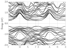
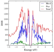
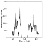
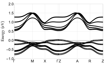
We computed the electronic band structure of \ceMn4Si7 using the Elk(elk, ) package. Details of the computation are listed in Appendix B. The band structure shown in Fig. 4a is insulating with a direct gap of 0.51 eV from the hole pocket below the Fermi level to the electron pocket at the point in the Brillouin zone The dispersion in the plane () is much the same as that in the plane (), due to the long -axis lattice constant and results in a electronic structure that is practically two-dimensional in nature. The magnitude of the gap in our calculations also compares well with experimental measurements(Gottlieb et al., 2003; Nishida, 1972).
The density of states (DOS) in Fig. 4b is comprised of \ceMn d-orbitals near the Fermi level and the \ceSi p - \ceMn d bonding orbitals are clustered in a region 2-5 eV below the Fermi level. Similar density of states with the -orbitals of the transition metal being the majority contributor to the states near the Fermi level has also been observed in band structure calculations for other NCL compounds(Yannello and Fredrickson, 2014).
The band structure and the DOS agree qualitatively with previous calculations by Migas et al. (2008) with weakly dispersing valence bands below the Fermi level that come from the \ceMn d orbitals. Quantitatively, they obtain a gap of 0.8 eV (see Fig.3 and Fig.5 in Ref.11) which is larger than our value of 0.5 eV. In experimental measurements, the band gap ranges from 0.42 to 0.98 eV(Mahan, 2004; Gottlieb et al., 2003; Nishida, 1972; Teichert et al., 1996; Rebien et al., 2002). Migas et al. (2008) also studied the band structures of \ceMn11Si19, \ceMn15Si26, and \ceMn27Si47 (see Fig.3 in Ref.11), where they obtained metallic ground states with the Fermi level lying within the valence bands. It was found that the dispersion near the Fermi level of these longer compounds is much like that of \ceMn4Si7 with the same energy gap from the top of the valence band to the bottom of the conduction band. The band structures of these longer -axis HMS show more pronounced two-dimensionality with almost identical dispersion in the and planes. The similarity in the band dispersion, the magnitude of the energy gap, and the enhanced two-dimensionality of these HMS lend further credence to the idea that these HMS are best thought of as stacked version of \ceMn4Si7 as described in Section II.2.
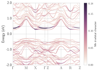
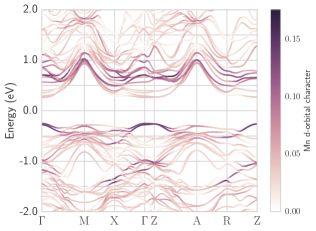
To further understand the band structure of \ceMn4Si7, we looked at the contribution of individual \ceMn sites to the bands. The unit cell of \ceMn4Si7 comprises of five distinct \ceMn sites as shown in Fig. 5a, where the first \ceMn atom is coloured red and is located at (0.0, 0.0, 0.0) and the fifth \ceMn atom in orange occupies (0.0, 0.0, 0.25). In Figs. 5b and 5c we depict the contributions to the band structure from the first \ceMn atom and the fifth \ceMn atom, respectively. Intriguingly, most of the contributions to the hole like bands come from the fifth Mn atom. In our structural picture of \ceMn4Si7 built by stacking half cells and then relaxing the positions of sterically unfavourable \ceSi atoms, this fifth Mn atom is equidistant from the interface at both and and is surrounded by \ceSi atoms that undergo the least relaxation.
This discrepancy in the relative contribution of the \ceMn atoms highlights the important role played by the \ceSi atoms in shaping the electronic band structure near the Fermi level. In the next subsection, we review some earlier results on the origin of the gap in the NCL compounds when there are 14 electrons per transition metal atom in the context of the HMS.
III.1 The origin of gap in NCLs - the 14 electron rule
Another common feature of a wide variety of NCLs (TtEm) is that most of them exhibit a gap in the band structure when there are 14 electrons per transition metal atom(Pearson, 1970; Lu et al., 2002). Fredrickson et al. (2004b) elucidated the origin of this gap with an analysis that combined DFT, Hückel theory, and the bonding between the transition metal atom and the main group element for a prototype compound with a \ceTiSi2 structure –\ceRuGa2. Much as in the case of \ceMn4Si7, the DOS near the Fermi level is dominated by the transition metal atom \ceRu in \ceRuGa2. In \ceRuGa2, the \ceRu atom is surrounded by a honeycomb of \ceGa atoms with a pair of \ceGa atoms lying both above and below the honeycomb plane. This structural motif underlies the analysis of the bonding between the \ceRu and \ceGa orbitals in \ceRuGa2. The gap at 14 electrons per T atom is related to the occupation of 14 orbitals per \ceRu atom. While the nature of the 14 orbitals and their distribution among \ceRu d, \ceRu-\ceGa bonding and \ceGa-\ceGa bonding vary depending on the -point in question, there is always a gap at this electron number.
The local environment of the fifth Mn atom in \ceMn4Si7 is very similar to that of \ceRu in \ceRuGa2, with the \ceMn atom surrounded by a honeycomb plane of \ceSi atoms and a pair of \ceSi atoms extending out of the honeycomb plane in either direction. As discussed in the previous section, the \ceSi atoms surrounding the fifth Mn atom are the ones undergoing the least structural distortion while \ceMn4Si7 is built from \ceMnSi2 and highlight how the structural underpinning of the 14 electron rule is carried over to \ceMn4Si7.
Later work on \ceRuGa2(Yannello and Fredrickson, 2014) suggests that the 14 electron rule is an instance of a more general rule for intermetallics compounds between a transition metal T and a main group element E. is identified to be the number of T-T bonds per T atom that are mediated by an E atom which in the case of a \ceTiSi2 structure as in \ceMnSi2 and \ceRuGa2 is four, thereby giving rise to the 14 electron rule.
In the case of the HMS, only \ceMn4Si7 has the requisite 14 electrons per \ceMn atom – 7 electrons from each \ceMn atom and 4 electrons from each \ceSi atom. In addition to explaining the band gap, the 14 electron rule also sheds light on why the other HMS are degenerate semiconductors. The electron count for each of the other HMS is a single electron short of the magic count of 14 electrons giving rise to a p-type band structure. Experimentally, the hole concentration is temperature independent at low temperature (Nishida, 1972) and ranges(Nishida, 1972; Teichert et al., 1996) from to . According to the 14 electron rule, the hole concentration is simply the number of holes in the unit cell and is summarized for the HMS in Table 1.
| \ceMn11Si19 | \ceMn15Si26 | \ceMn27Si47 | |
|---|---|---|---|
| Holes per unit cell | 4 | 2 | 4 |
| Unit cell volume ( cm3) | 1.46 | 2.0 | 3.61 |
| Hole density ( cm-3) | 2.74 | 1.0 | 1.11 |
IV Effective Tight-binding model for HMS
In previous sections, we highlighted how the electronic band structure of the HMS is mostly comprised of \ceMn -orbitals with the \ceSi -orbitals playing a supporting role. In addition, we also pointed out how the structure of \ceMn4Si7 can be built up from half cells. In this section, we will combine these two insights to model the band structure of the HMS via tight-binding.
The predominance of \ceMn -orbitals suggests that we might be able to model the electronic band structure (at least near the Fermi level) in terms of a model consisting solely of \ceMn orbitals. This does not mean that the Si atoms are unimportant. The hopping integral between Mn atoms are dependent on the intervening Si atoms, and we will discuss them later. Typically in transition metal oxides, the crystal field splitting from the ions provides us with a degenerate set of local orbitals on the transition metal atom, but in the HMS, the mismatch between the periods of the \ceSi and \ceMn atoms means that we do not have a regular local coordination for the \ceMn atoms. We consider instead, an effective model for the band structure of the HMS with two spherically symmetric orbitals on each \ceMn site. In the next subsection, we elaborate on the construction of this model for \ceMn4Si7.
IV.1 Tight-binding model for \ceMn4Si7
As pointed out in Section II.1, the unit cell of \ceMn4Si7 is made up of two half-cells with five distinct \ceMn atoms each. The symmetry related atoms within the unit cell are coloured the same in Fig. 5a, and Fig. 6a shows the unit cell once it has been split into two half-cells; the atoms belonging to the bottom half-cell denoted with colored circles and those in top half-cell denoted with dark borders for the colored circles. The actual positions of the distinct atoms in the unit cell are listed in Section C.1, but to simplify the our model, the fractional positions of the atoms along the axis are modified to be at integer multiples of .
In the following sections, we will discuss a model where the structure is assumed to be of the type as shown in Fig. 6a with two subunits of five distinct sites each (shown in Fig. 5a in the unit cell).
IV.1.1 Overlaps within the half-cell
Our model consists of two orbitals on each Mn site that are separated by a gap to mimic the behaviour of the valence and conduction bands. The two orbitals have the same kind of overlaps, but we allow for the magnitudes of the overlaps to be different. The various overlaps are briefly described here, more details are in Section C.1.1.
Within each half-cell, our model includes seven different types of \ceMn-\ceMn overlaps – the first three are the nearest (N), the next-nearest (NN), and the third-nearest neighbour (NNN) overlaps. The next three are further neighbour overlaps for atoms located in the same plane The final overlap is between Mn atoms that are directly above one another along the -direction. We denote the magnitudes of these overlaps by parameters .
IV.1.2 Overlaps between half cells
The two half-cell nature of the structure is incorporated into our model by supplementing the single half-cell model in the previous section with an additional hopping parametrized by between atoms that are situated half a lattice vector along the -axis. The hopping hamiltonian for each orbital is then represented in block form as
| (3) |
where is the hopping for the single half-cell, and is the hopping between the subunits.
For the valence bands, we find that a parameter set
| (4) | ||||
| (5) |
in units of meV for the hoppings within the subunit and an additional hopping parameter meV for the hopping between half cells provides us with a good match to the DFT band structure. The hopping between the subunits is chosen to match the estimated splitting between the top two valence bands.
The conduction bands are modeled by modifying the magnitudes of all the hoppings in Eq. 3 to obtain a Hamiltonian denoted by . The conduction band parameters are given by the set (we use to distinguish between valence and conduction band parameters)
| (6) | ||||
| (7) |
Our phenomenological model for \ceMn4Si7 contains two effective orbitals that are separated by a gap to give rise to a Hamiltonian of the form
| (10) |
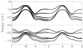
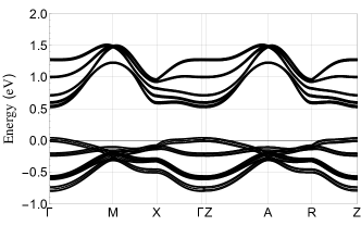
The band structures of our model is shown in Fig. 7. Considering the relative simplicity of our tight-binding model, the agreement between our band structure (which is constructed to model the bands near the Fermi level) and the one from DFT is remarkable. We are able to reproduce most of the features of the band structure for the valence bands namely the two fold hole pocket at the point and the degeneracies at the and the points. The conduction bands near the Fermi level are also well reproduced
The set of parameters employed to obtain this fit needs some elaboration given that we only considered overlaps between \ceMn sites. The validity of the 14 electron rule in \ceMn4Si7 and the contributions of the fifth Mn atom to the bands near the Fermi level are both due to the bonding between Si and Mn atoms. While further calculations based on methods such as projections to Wannier orbitals are needed to underpin the exact contribution of the Si atoms to the band structure, a few key aspects can be readily inferred from the parameter set detailed above. Given that the \ceMn atoms are composed of 3 orbitals which are quite localized, we would expect that the direct overlaps between the \ceMn orbitals would be quite small and this is indeed reflected in our tight-binding parameters where the largest overlap is only about 50 meV. The intervening Si atoms are expected to play a role in the surprisingly large further neighbour overlaps in the plane which are comparable to the nearest-neighbour overlaps111These hoppings are crucial for obtaining a good fit within our model. Also see Chapter 5 in (Vijay Shankar, 2016).
Fig. 7 compares the band structure of the model for \ceMn4Si7 with no further neighbour hoppings (). As the magnitudes of these terms are increased in the model, the effective mass of the holes in the valence band increases (valence bands become flatter) and that of the electrons in the conduction decreases near the point. In addition, the valence and conduction bands are pushed further down at the (and ) points. Applying pressure along the -axis should decrease the overlaps between orbitals in the plane compared to the overlaps along leading to decrease in effective mass for the valence band holes and increase for the conduction band electrons.
IV.2 Modeling the HMS band structure – stacking a model for \ceMn4Si7
We now proceed to discuss how we use our tight-binding model for \ceMn4Si7 described in the previous section, to model the other HMS. We have previously discussed how structurally these compounds can be built by stacking many halfcells of \ceMn4Si7. Given that the stacking is along the -axis, we employ an approach very similar to the one we described for \ceMn4Si7 – add a small hopping term (equal to ) between the same sublattice in adjacent subunits. The stacking also increases the -axis lattice constant by a factor equal to the number of \ceMn4Si7 units (say ) in the stacked unit cell and correspondingly modifies all the hopping terms described in Section IV.1.1 which have a dependence by replacing by .
Mn11Si19 is modeled by stacking three \ceMn4Si7 unit cells or six half cells along the axis. The overlap within the half cells remain the same and those between the half cells has the same form as that discussed in Section IV.1, with overlaps only between neighbouring half-cells. Since the -axis lattice constant is now three times that of the orginal case for \ceMn4Si7, all the dependent hopping terms in Section IV.1.1 are modified by changing .
In a similar vein, \ceMn15Si26 is modeled by stacking four unit cells (or eight half cells) of \ceMn4Si7 along the -axis, and modifying the dependence () for all the hopping terms outlined in Section IV.1.1.
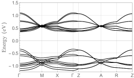
The band structures for \ceMn11Si19 and \ceMn15Si26 are shown in Fig. 8 with the Fermi level chosen by ensuring that when the valence bands are filled, the 14 electron rule is obeyed. As mentioned in Section III.1, both \ceMn11Si19 and \ceMn15Si26 are one electron short of having 14 electrons per \ceMn atom. The Fermi level is thus within the valence bands for these two compounds. Our simple model is thus able to capture the main feature of the band structure of these compounds, namely a hole pocket near the and points. The many half cells give rise to many bands crossing the Fermi level and the small hopping between the half cells is reflected in the small splitting between these bands.
As pointed out in Section II.2, the -axis lattice constant for the \ceMn11Si19 and \ceMn15Si26 is smaller than the one predicted by the rule. For our tight-binding model, this decrease in the -axis lattice constant would translate to a slight increase in the hopping along this direction, resulting in bands that would disperse slightly more along the c-axis. The overall features of the band structure will still remain the same because the -axis dispersion is quite small to begin with.
V Discussion and Conclusions
Our minimal tight-binding model for the band structure of the HMS posits that the high effective mass is due to further neighbour hoppings between the \ceMn atoms. This could be tested by measuring the effective mass or the Seebeck coefficient under pressure applied along the -axis. Under this kind of pressure, the plane overlaps are expected to decrease relative to the other overlaps and should present itself as a decreased effective mass for the valence bands. Tensile strain along the -axis, on the other hand, increases the plane overlaps relative to the others and will result in a higher effective mass. The Seebeck coefficient is proportional to the effective mass through the Pisarenko relation, and straining the HMS might be a route to increasing the Seebeck coefficient and possibly also the thermoelectric figure of merit ZT.
Compressive and tensile strain along the -axis should also impact the electrical conductivity as it changes both the effective mass and the velocity of the electrons near the Fermi level. From our tight-binding band structure, tensile strain along the -axis increases the plane hopping relative to the others resuling in an increase in both the effective mass and the electron velocity at the point, which presumably results in a higher electrical conductivity within a Boltzmann type approach. Indeed, a recent preprint(Cuong et al., 2016) that appeared while this manuscript was being prepared for publication, used density functional theory to study the effect of strain on \ceMn4Si7reports that the plane conductivity decreases under tensile strain along the plane and increases under compressive strain. Although they do not consider the effect of strain along the -axis on the plane, their results are broadly consistent with our tight-binding picture as we expect the plane hopping parameters to increase under plane compressive strain resulting in an increased electrical conductivity conductivity.
Another report describing the preparation of \ceMnSi2 phase in thin films also appeared recently(Shin et al., 2015). The measured lattice constants in Shin et al. (2015) are quite similar to that of \ceMn4Si7 and the measured electronic properties (Seebeck, resistivity) are similar to that of \ceMn11Si19. The result is tantalizing given our model for the HMS as being built from \ceMnSi2 cells, and it would be interesting to calculate the electronic band structure of the \ceMnSi2 structure and compare it with that of the HMS.
In summary, using a combination of structural arguments, and electronic structure calculations, we have constructed a minimal tight-binding model for the HMS. Our main results are as follows: all the HMS can be constructed from \ceMn4Si7 which itself is built by stacking two half-cells of a compound with stoichiometric formula \ceMnSi2 along the axis. The band structure of \ceMn4Si7 in electronic structure calculations is insulating with a gap of 0.51 eV broadly in agreement with experiments and previous theoretical calculations. A closer look at the contribution of the different \ceMn atoms to the valence bands reveals that the \ceMn atom that is least affected by rearrangement at the interfaces, is the majority contributor. The 14 electron rule provides an estimate for the charge density in the HMS and is remarkably close to measured values. Our minimal tight-binding model consisting of effective -orbitals on \ceMn atoms is able to capture most of the features of the band structure of \ceMn4Si7 and can be easily extended to model the band structure of the other HMS. The modeling of the thermoelectric properties of the HMS using the tight-binding model presented in this paper will be addressed in forthcoming work.
Acknowledgements - This work was supported by NSERC of Canada through the HEATER program and the center for Quantum Materials at the University of Toronto. Computations were performed on the GPC supercomputer at the SciNet HPC Consortium. SciNet is funded by: he Canada Foundation for Innovation under the auspices of Compute Canada; the Government of Ontario; Ontario Research Fund - Research Excellence; and the University of Toronto. VSV thanks the NSERC CREATE HEATER program for a fellowship.
Appendix A Crystal structure of \ceMn4Si7
| Spacegroup: Pc2 (no. 116) | |||||
| Lattice constants: a=b=5.52590 Å, c= 17.5156 Å | |||||
| Atom | x | y | z | Wyckoff | Symmetry |
| Mn1 | 0.00000 | 0.00000 | 0.00000 | 2c | -4.. |
| Mn2 | 0.50000 | 0.00000 | 0.06508 | 4i | 2.. |
| Mn3 | 0.50000 | 0.50000 | 0.12939 | 4h | 2.. |
| Mn4 | 0.00000 | 0.50000 | 0.19137 | 4i | 2.. |
| Mn5 | 0.00000 | 0.00000 | 0.25000 | 2a | 2.2 2 |
| Si1 | 0.15715 | 0.20150 | 0.11253 | 8j | 1 |
| Si2 | 0.32270 | 0.84419 | 0.18189 | 8j | 1 |
| Si3 | 0.33130 | 0.33130 | 0.25000 | 4e | ..2 |
| Si4 | 0.34518 | 0.22740 | -0.03800 | 8j | 1 |
Appendix B Computational Details
The Elk package (elk, ), which implements the Full-Potential Linearly Augmented Plane Wave (FP-LAPW) method was used for the electronic structure calculations. The Perdew-Zunger parametrization of the local density approximation (LDA) was chosen for the exchange-correlation functional(Perdew and Zunger, 1981). The muffin-tin radii were automatically determined by the elk code to be 1.988 and 1.822 a.u.for Manganese and Silicon, respectively. For Brillouin zone intergration we used the highq option in Elk, which resulted in a -point grid of 552 corresponding to 12 points in the irreducible part of the Brillouin zone. Spin-orbit coupling and spin polarization were both ignored in our calculations.
Appendix C Details of the tight-binding model
In this section, we provide more details of our tight-binding model including descriptions of the various terms in the tight-binding Hamiltonian. First, we describe the modified positions of the five different Mn atoms in our tight-binding unit cell and then we describe the various overlaps and the associated hopping matrices in our tight-binding model.
C.1 Modified Mn positions
The five different Mn atoms occupy positions that are very close to multiples of as listed in Table 2. For our tight-binding model, we shifted the atom positions to integer multiples of .
| Atom Type | Modified positions in unit cell |
|---|---|
| Mn1 | (0,0,0), (0., 0, ) |
| Mn2 | (,0,), (0, , ), (,0, ), (0, , ) |
| Mn3 | (0, , ), (0, , ), (0, , ), (0, , ) |
| Mn4 | (0, , ), (, 0, ), (0, , ), (0, , ) |
| Mn5 | (0, 0 , ), (0, 0 , ) |
C.1.1 Tight-binding overlaps
Within each half-cell, we considered seven different types of overlaps – the first three are the nearest (NN), the next-nearest (NN) and the third-nearest neighbour (NNN) overlaps. For each site, the nearest-neighbours are situated a fractional distance () and () or with the axis fractions interchanged among the and directions. The magnitude of this overlap was denoted and is depicted in Fig. 6a. Employing a basis , where creates an electron in the orbital at site , the NN hopping Hamiltonian is , and the matrix given by
| (16) |
where with
The next-nearest neighbours for each site are a pair of atoms situated at () and another pair at () or with and positions interchanged among these pairs. The magnitude of this hopping is also depicted in Fig. 6a. The matrix obtained for this overlap is
| (22) |
where with .
The third-nearest neighbours involved in the overlap for each site are at () along the [111] direction and give rise to a hopping matrix with the form
| (28) |
where
Fig. 6a also depicts the overlap ( from an atom to another one directly above it along the axis at a distance . The matrix is given by
| (34) |
where .
The next three overlaps are overlaps between atoms situated in the same plane and are labelled and . and were depicted in Fig. 6b. The overlap between atoms situated a lattice vector apart in the plane, which we call hab1 is
| (40) |
where
The overlap between atoms that are at a distance () apart was denoted , and the associated matrix is given by
| (46) |
where .
The last overlap within a half-cell is between atoms situated two lattice vectors apart in the plane denoted with the matrix given by
| (52) |
where
The factor of two for some of the atoms (2, 3, and 4) is because within each subunit, there are two instances of those atoms. Including all the different kinds of overlaps, the full hamiltonian for the single subunit pictured in Figure 5a is
| (53) |
The additional hopping between the same atom in different half-cells was denoted by in Fig. 6a and is associated with a matrix given by
| (59) |
References
- Nowotny (1970) H. Nowotny, in Chem. Ext. defects non-metallic solids, edited by L. Eyring and M. O’Keeffe (1970) pp. 223–237.
- Bost and Mahan (1987) M. Bost and J. E. Mahan, J. Electron. Mater. 16, 389 (1987).
- Kawasumi, I., Sakata, M., Nishida, I. & Masumoto (1981) K. Kawasumi, I., Sakata, M., Nishida, I. & Masumoto, J. Mater. Sci. 16, 355 (1981).
- Gottlieb et al. (2003) U. Gottlieb, A. Sulpice, B. Lambert-Andron, and O. Laborde, J. Alloys Compd. 361, 13 (2003).
- Schwomma et al. (1964) O. Schwomma, a. Preisinger, H. Nowotny, and a. Wittmann, Monatshefte fur Chemie 95, 1527 (1964).
- Knott et al. (1967) H. W. Knott, M. H. Mueller, and L. Heaton, Acta Crystallogr. 23, 549 (1967).
- Zwilling and Aus (1973) V. G. Zwilling and N. Aus, 675, 668 (1973).
- De Ridder and Amelinckx (1971) R. De Ridder and S. Amelinckx, Mater. Res. Bull. 6, 1223 (1971).
- Nishida (1972) I. Nishida, J. Mater. Sci. 7, 435 (1972).
- Krontiras et al. (1988) C. Krontiras, K. Promoni, and M. Roilos, J. Phys. D. Appl. Phys. 21, 509 (1988).
- Migas et al. (2008) D. Migas, V. Shaposhnikov, a. Filonov, V. Borisenko, and N. Dorozhkin, Phys. Rev. B 77, 1 (2008).
- Fredrickson et al. (2004a) D. C. Fredrickson, S. Lee, R. Hoffmann, and J. Lin, Inorg. Chem. 43, 6151 (2004a).
- Fredrickson et al. (2004b) D. C. Fredrickson, S. Lee, and R. Hoffmann, Inorg. Chem. 43, 6151 (2004b).
- (14) “http://elk.sourceforge.net,” .
- Ye and Amelinckx (1986) H. Ye and S. Amelinckx, J. Solid State Chem. 61, 8 (1986).
- Fredrickson (2005) D. C. Fredrickson, the Nowotny Chimney Ladder Phases : the Role of Electron Counts and Interfaces in the Stability of Intermetallic Compounds, Ph.D. thesis, C (2005).
- Yannello and Fredrickson (2014) V. J. Yannello and D. C. Fredrickson, Inorg. Chem. 53, 10627 (2014).
- Mahan (2004) J. E. Mahan, Thin Solid Films 461, 152 (2004).
- Teichert et al. (1996) S. Teichert, R. Kilper, J. Erben, D. Franke, B. Gebhard, T. Franke, P. Häussler, W. Henrion, and H. Lange, Appl. Surf. Sci. 104-105, 679 (1996).
- Rebien et al. (2002) M. Rebien, W. Henrion, H. Angermann, and S. Teichert, Appl. Phys. Lett. 81, 649 (2002).
- Pearson (1970) W. B. Pearson, Acta Crystallogr. Sect. B Struct. Crystallogr. Cryst. Chem. 26, 1044 (1970).
- Lu et al. (2002) G. Lu, S. Lee, J. Lin, L. You, J. Sun, and J. T. Schmidt, J. Solid State Chem. 164, 210 (2002).
- Note (1) These hoppings are crucial for obtaining a good fit within our model. Also see Chapter 5 in (Vijay Shankar, 2016).
- Cuong et al. (2016) D. D. Cuong, J. Park, S. H. Rhim, and S. C. Hong, ArXiv e-prints (2016), arXiv:1605.03684 [cond-mat.mtrl-sci] .
- Shin et al. (2015) Y. Shin, S. H. Rhim, A. T. Duong, V. Q. Nguyen, S. C. Hong, S. Cho, and H.-M. Park, J. Vac. Sci. Technol. A Vacuum, Surfaces, Film. 33, 061516 (2015).
- Perdew and Zunger (1981) J. P. Perdew and A. Zunger, Phys. Rev. B 23, 5048 (1981).
- Vijay Shankar (2016) V. Vijay Shankar, Perspectives from ab-initio and tight-binding: Applications to transition metal compounds and superlattices, Ph.D. thesis, University of Toronto (2016).