Plasmon-assisted photoresponse in Ge-coated bowtie nanojunctions
Abstract
We demonstrate plasmon-enhanced photoconduction in Au bowtie nanojunctions
containing nanogaps overlaid with an amorphous Ge film. The role of
plasmons in the production of nanogap photocurrent is verified by
studying the unusual polarization dependence of the photoresponse.
With increasing Ge thickness, the nanogap polarization of the photoresponse
rotates 90 degrees, indicating a change in the dominant relevant plasmon
mode, from the resonant transverse plasmon at low thicknesses to the
nonresonant “lightning rod”mode at higher thicknesses. To understand
the plasmon response in the presence of the Ge overlayer and whether
the Ge degrades the Au plasmonic properties, we investigate the photothermal
response (from the temperature-dependent Au resistivity) in no-gap
nanowire structures, as a function of Ge film thickness and nanowire
geometry. The film thickness and geometry dependence are modeled using
a cross-sectional, finite element simulation. The no-gap structures
and the modeling confirm that the striking change in nanogap polarization
response results from redshifting of the resonant transverse mode,
rather than degradation in the Au/Ge properties. We note remaining
challenges in determining the precise mechanism of photocurrent production
in the nanogap structures.
keywords:
Plasmonics, optoelectronics, nanogap, polarizationDepartment of Physics and Astronomy]Department of Physics and Astronomy \alsoaffiliation[Department of Electrical and Computer Engineering]Department of Electrical and Computer Engineering, Rice University, Houston, Texas 77005 \phone(713) 348-3214
Light coupled into surface plasmons in metallic nanostructures can generate extremely large enhancements to the local electromagnetic field. Optical antennas exploit the resonant behavior and large scattering cross section of plasmons in nanostructured metals for use in a wide variety of applications including surface-enhanced Raman spectroscopy (SERS)1, 2, subwavelength optics3, 4, plasmonic optical trapping5, 6, 7, 8, and plasmon-assisted light harvesting9, 10, 11, 12, 13, 14, 15, 16, 17. Photosensitive devices utilizing plasmonic nanoantennas generate photocurrent through two dominant mechanisms: Near-field photons can be absorbed in a nearby semiconductor to create electron-hole pairs; or high-energy (“hot”) electrons generated by the plasmon can tunnel across a semiconductor-metal potential barrier, directly resulting in photocurrent. Plasmonically active devices often have the benefit of being highly polarization dependent, operational at small biases, and capable of being fabricated with photoactive elements on a scale smaller than the wavelength of the incident light.
Gold “bowtie” nanojunctions, consisting of a nanowire (with or without a nanogap) connected by two extended leads, have been shown to act as combined optical antennas and electrical probes18. The plasmon response in this geometry is dominated by a transverse dipolar mode, resonant for incident light polarized perpendicular to the length of the constriction. In devices with nanogaps at their center, made through either electromigration or via a multi-step “self-aligned” lithographic technique19, the transverse plasmon mode hybridizes with multipolar “dark” modes at the gap edges to form a strong electromagnetic field enhancement at the junction center, or “hotspot”. The SERS response of molecules assembled into these hotspots follows the signature polarization dependence of dipolar optical antennas, with maximum response perpendicular to the axis of the constriction20. This is in contrast to expectations of the nonresonant “lightning rod” effect, when the maximum plasmon response occurs when the incident polarization parallel to the elongated direction of a metal wire or tip, from the excitation of longitudinal or tip plasmons21.
In no-gap bowtie nanowires, resonant laser illumination produces a polarization-dependent hotspot via photothermally induced changes in resistivity22. Direct absorption and the excitation of the transverse plasmon mode locally increase the temperature of the nanowire, decreasing its conductance, , due to the temperature-dependent resistivity of the metal. The polarization dependence of this change is also dipolar, so that the temperature of the nanowire increases more for the transverse excitation, even without the existence of gap plasmons. This measurement provides a convenient measurement technique to assess the plasmon response of the nanowire material itself.
In this report, we study the photoresponse of bowtie nanoantennas overlaid with a thin Ge film. We examine the plasmon-assisted photoconduction () in bowties with nanogaps. At low Ge thicknesses, we find that the photoconductance is maximal with incident polarization transverse to the nanowire; in contrast at higher Ge thicknesses, the maximum photoconductance occurs when the incident polarization is rotated by 90 degrees. The Ge thickness alters which plasmon response is dominant in the nanogaps, the resonant transverse mode (at low thicknesses) or the nonresonant “lightning rod” response (at high thicknesses). A concern is whether the transverse plasmon mode is eliminated entirely due to degradation of the Au properties with thicker Ge layers. To test for this, we also measured the plasmon-induced heating in unbroken (no-gap) nanowires (). We find experimentally, and in accord with a computational model, that the presence of Ge predictably redshifts the resonance of the nanoantenna’s transverse plasmon mode without degrading the Au plasmonic response. The manipulation of resonant and nonresonant plasmon responses is an interesting avenue to consider in further plasmonic optoelectronic structures.
This work is one of a handful demonstrating plasmon assisted photocurrent in individual nanoantennas. Unlike similar work integrating photosensitive materials, such as graphene23, 24, MoS225, and traditional semiconductors26, 27, 28, 29, into plasmon resonant geometries, the nanogap devices reported in this study rely on a truly nanoscale active optical region, typically 100 5 10 , fabricated from amorphous Ge, an abundant and easily deposited material. Other schemes for fabricating field enhanced photodetectors and photovoltaic devices have been discussed in depth over the past five years3, 30, 31, 32. This report builds upon recent work outlining the strength of non-radiative, hybridized plasmon modes in bowtie nanoantennas.
Methods
The devices in this report are fabricated on n-type Si wafers with a 200 thermally grown oxide layer. Electron beam lithography is used to define the nanowire constriction and small triangular electrodes, which extend to larger, prefabricated Au contact pads deposited using a shadowmask. After development, a 1 Ti adhesion layer and 13 of Au are deposited by electron beam evaporation, followed by lift-off in acetone. Nanowires are patterned to be 600 long and vary from 80 to 140 wide depending on the desired geometry.
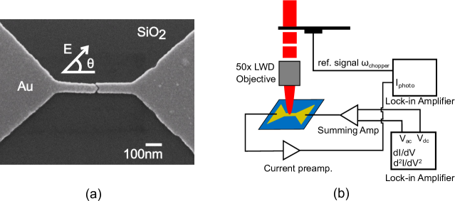
In the case of “self-aligned” nanojunctions, an extra step of lithography is needed to create the gap19. In the first step, the left half of the nanowire is patterned and the 1 / 13 Ti/Au combination is deposited, followed by a 1 layer of \ceSiO2 and 14 layer of Cr. After the metal deposition, exposing the sample to air creates a layer of Cr-oxide which swells to extend just past the edge of the pattern, acting as a shadowmask in the second evaporation. The layer of \ceSiO2 prevents Cr and unwanted elements of the Cr etchant (namely cerium) from contaminating the Au and potentially degrading device plasmon response. During a second lithographic step, the right half of the pattern is aligned to the existing left half. An identical evaporation follows with the same materials and thicknesses, to ensure device uniformity. The Cr and \ceSiO2 are etched away, leaving a 2-10 gap between the two sides of the nanowire where the oxidized Cr expanded beyond the first pattern (1a). The width of the gap can be tailored by adjusting the thickness of the Cr layer19.
The devices are cleaned with \ceO2 plasma and wirebonded to a chip carrier. Each device is scanned with a 785 diode laser configured with a telescopic lens rastering system to create a spatial map of the photoresponse. The laser has a Gaussian beam profile with a full width at half-maximum of approximately 1.8 , operating in CW mode at a typical laser power of 3-4 reaching the sample. A lock-in amplifier, synched to an optical chopper at a frequency of 281 , is used to measure device optical response: either the photocurrent generated in self-aligned devices () or the optically induced change to the conductance in no-gap nanowires (). The sample is biased with the summed output of the desired dc voltage, typically up to 0.2 , and a 10 RMS ac voltage, and a second lock-in, at frequency 789 , measures the first- and second-order differential conductance ( and ). The dc current () is measured using a digital-to-analog converter (DAC) built into one of the lock-in amplifiers (1b). After each scan, the laser is then finely positioned at the hotspot center by maximizing or , the polarization is rotated continuously from to (with defined to be along the nanoantenna long axis) using a motorized half-wave plate, and the optical and electrical responses are measured. Bare bowtie nanowires (with and without nanogaps) are coated with an amorphous Ge film of varying thickness deposited by electron beam evaporation, and remeasured using the same procedure. All measurements presented in this paper were conducted at room temperature at a pressure on the order of 100 .
Results
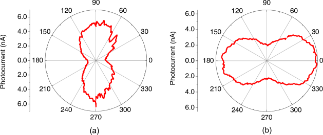
Photoresponse of the self-aligned nanogap junctions is dominated by a positive photoconductance of the Ge in the gap region. Photocurrent measurements of self-aligned nanojunctions present two distinct polarization dependences. In devices with a nanowire width of 80 and a 10 Ge film, the photocurrent follows the signature dependence of dipolar optical antennas, with maximum response at (2a). Repeating this experiment with 130 wide nanowire and a thicker layer of Ge (35 ) shifts the polarization dependence by (2b). In both cases, photocurrent is linear with respect to laser power and dc bias, and only occurs at the junction center.
To understand this, we consider the plasmons in the system. In previous work exploring photoresponse in bowtie nanoantennas, it has been demonstrated that the greatest field enhancement occurs when incident light is polarized perpendicular to the nanowire axis, corresponding to a strong dipolar transverse plasmon mode20. For bare Au nanowires, this mode is known to be resonant at 785 for bare nanowires ~130 wide and 13 thick. It would appear that in the narrower-wire nanogap devices with the thinner Ge film, the photocurrent is dominated by this transverse plasmon response, while for the wider-wire nanogap devices with thicker Ge the dominant plasmon response is that of the nonresonant longitudinal “lightning rod” mode.
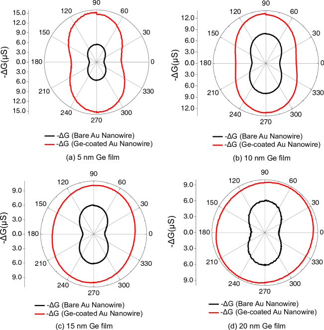
An issue is whether, in the thicker Ge devices, the plasmonic properties of the Au itself is degraded (e.g., through partial alloying with the Ge due to the longer deposition), or whether the change in the plasmon response is due purely to shifting of the resonant transverse mode away from the operating wavelength. To understand this dramatic change in nanogap device plasmon response, we fabricate “unbroken” no-gap nanowires, and assess the plasmonic properties of the Au through study the photothermally induced change in the conductance, (due to the temperature-dependent Au resistivity), as a function of nanowire width and Ge film thickness. Measurements on bare Au bowtie nanowires (~130 wide and 13 thick) are consistent with previous work measuring resistive heating in these structures; the conductance change includes a characteristic polarization dependent contribution, with a maximum at due to the contribution to heating from the structure’s transverse plasmon mode. 22. This indicates that the laser wavelength is on resonance with the transverse mode of the nanowire (width ~130 , thickness 13 ), heating it approximately by 2-10 depending on the exact width of the device and the incident laser power. The increase in temperature can be estimated directly from the change in conductance using the formula provided in Herzog, et. al. (2014), , where is the resistance of the device and for these Au bowtie nanowires. This value has been measured to be consistent for many nanowire devices.
After each initial characterization of bare devices, a Ge film of varying thickness (5 , 10 , 15 , and 20) is deposited by electron beam evaporation and the photoresponse is remeasured (3). For each trial, the polar plots become progressively more circular, as the increasing thickness of Ge redshifts the resonance of the transverse plasmon mode away from the laser wavelength of 785 . The data are fitted to the expression . Here, is the nonresonant, direct absorption contribution, while is the component of the conductance change due to dipolar plasmon-based heating. The ratio then gives a measure of the transverse plasmon contribution to the change in conductance for each thickness trial. This ratio is roughly constant for bare junctions across all four trials, but steadily decreases in the presence of increasing Ge film thickness (4a). By 20 of Ge, the devices lose all their polarization dependence; their polar plots become entirely circular, indicating that the presence of the film has shifted the transverse plasmon mode far off-resonance, removing the dipolar response of the nanoantenna, and leaving behind only heating from nonresonant absorption.
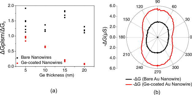
To verify that the dominant effect on the polarization is redshifting of the plasmon resonance rather than simple attenuation of the plasmon resonance due to Au degradation, we fabricated intentionally off-resonance nanowires, less than 100 wide, and then deposited a Ge film to redshift the resonance back to the laser wavelength. The pre- and post-Ge deposition bowties are analyzed following the above procedures (4b). In this case we see the ratio increase, indicating that the polarization dependence of the junction becomes more dipolar in the presence of the Ge film. This effect was found to be consistent in 8 measured devices.
These experiments verify that for the gapped nanojunctions a 35 Ge film will remove the transverse plasmon mode’s contribution toward the photocurrent for a device previously on resonance with the laser wavelength, as seen in 2b. For structures made off resonance with the laser, adding an appropriately thick layer of Ge can tune the device back onto the laser wavelength, as seen in 2a. To map out the appropriate thicknesses of Ge over a range of device widths, the resonance of the transverse plasmon mode in nanoantennas was modeled with a finite-element software package designed to solve differential equations over physical spaces (FEM, COMSOL 3.5a). A cross-sectional model was designed so that the incident light is polarized perpendicular (transverse magnetic mode) to an infinitely long nanowire, isolating the transverse plasmon mode for the purposes of this study (5a). Ge is known to be entirely amorphous when deposited by evaporation with the substrate at room temperature, and accordingly a dielectric function for amorphous Ge was used in the model33, 34. The dielectric function for Au was taken from Johnson and Christy35. Maxwell’s equations are solved over the entire solution space as a function of nanowire width and Ge film thickness. For an incident plane wave with free space wavelength ranging from 400 to 1500 , a scalar proportional to the optically driven resistive heating is found by integrating resistive heating over the area of the Au, where is the electrical conductivity and is the norm of the total electric field (5b). As the film thickness increases, the original resonance is redshifted and broadened, as expected from previous work exploring plasmon modes in the presence of semiconductors36, 10, 37. Bare devices with transverse modes previously resonant at the laser wavelength of 785 will be shifted off resonance further into the near-IR in the presence of a 5-10 film of Ge.
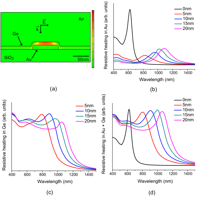
This simple model provides a proof-of-concept explanation for the shift in the resonance of the transverse plasmon mode, but does not take into account heating from absorption in the Ge layer; it assumes that all photothermally induced change in current comes from heating in the Au alone. This calculational omission accounts for the predicted decrease in the magnitude of the peaks for increasing Ge thickness not seen in the experiment. In contrast, in the measurements the photothermal heating in unbroken bowtie nanowires is larger with the Ge film than without it (ie. of the Au is always larger for Ge-coated nanowires than for bare nanowires). Integrating the variable over the volume of the Ge film produces a broad plateau at a wavelength below the plasmon resonance due to direct absorption in the Ge overlayer (5c). Adding the two spectra for together (ie. 5b + 5c) results in resonance peaks of Ge-coated nanowires with magnitudes for the structure’s total optically driven resistive heating comparable to the magnitude of bare junctions (5d). Extracting precise predictions for the Au temperature increase in Ge-coated nanowires under laser illumination would require knowledge of both the thermal boundary resistance at the interface between the Ge at the Au, and the thermal conductance of the amorphous Ge.
Discussion
We have found that the change in polarization response of the photoconductive nanogap antennas with Ge thickness is caused by the tuning of which plasmons dominate at the incident wavelength, the resonant transverse mode or the nonresonant “lightning rod” response. In either limit we have not addressed the precise mechanism of the positive photoconductance of the Ge-coated nanogap structures. There are several potential mechanisms which could contribute to the photocurrent generated in the Ge-coated nanogap structures: direct absorption of light in the Ge located at the gap creating electron-hole pairs via the photovoltaic effect (PVE); driving “hot” carriers generated in the plasmon across the semiconductor-metal barrier, also known as direct electron transfer (DET); or through plasmon-induced resonant energy transfer (PIRET), where the plasmon can directly excite electron-hole pairs in the Ge38, 39. Similar studies have also reported photocurrent generation due to the photothermoelectric effect (PTE)40, 25 and optical rectification23, 41. In this study, photocurrent generation only occurs at the nanojunction center, not along the length of the nanowire, and therefore cannot be due to PTE. Additionally, the photocurrent does not trace the signature nonlinear electrical response for optical rectification, . Therefore the photocarriers in Ge-coated bowtie nanojunctions must be generated by a combination of field-enhanced PVE in the Ge and by plasmonic coupling between the Au and the Ge through DET or PIRET. DET has been reported in various plasmon-based photovoltaic devices, but device responsivity is typically inefficient because collection of hot carriers requires careful engineering of geometry and materials to ensure effective coupling between the plasmon, absorption medium, and electrodes17, 11, 32, 30. The measured responsivity in theGe-coated nanogaps in this works calculated to be ~10-6 at 0.2 which is comparable to the values listed in Shi, et. al. (2011), who use electromigrated bowtie nanoantennas on top of graphene, but is significantly lower than the values reported by Tang, et. al. (2008). However, their device has a much larger active area and uses crystalline Ge. All three potential mechanisms would have identical polarization dependences; higher fields would produce larger enhancements and more hot carriers, making it difficult to distinguish between the these mechanisms based on photoresponse measurements alone. Spectral data or time-resolved measurements could shed light on the relative contribution of each process due to the characteristically short lifetime of hot electrons.
Bowtie nanowires provide a platform for understanding plasmon response in individual metal-semiconductor-metal nanoantennas. We provide experimental and computational evidence that the dominant plasmon modes in such structures may be controlled by tuning between resonant and nonresonant responses. Photocurrent measurements of Ge-coated nanogap structures dominated by the resonant transverse mode are consistent with measurements of unbroken bowtie nanowires; polarization dependence in both cases follows the known polarization dependence of dipolar optical antennas, with peak photoresponse occurring at an excitation perpendicular to the length of the nanowire (). By optimizing device geometry, this resonant response may be “tuned away” without degrading the Au properties, leaving behind the nonresonant, longitudinal “lightning rod” mode. The nanogap devices operate with a truly nanoscale active region defined by the volume of the interelectrode nanogap. Knowledge of the impact of dielectrics on both resonant and nonresonant local plasmon-enhanced fields is an important step toward fabricating efficient nanoscale light harvesting devices.
K.M.E. would like to acknowledge Robert A. Welch Foundation award C-1636 and thank Will Hardy and Yajing Li for useful discussions during the completion of this project. P.Z. and D.N. acknowledge support from ARO award W911-NF-13-0476.
References
- Ward et al. 2007 Ward, D. R.; Grady, N. K.; Levin, C. S.; Halas, N. J.; Wu, Y.; Nordlander, P.; Natelson, D. Electromigrated Nanoscale Gaps for Surface-Enhanced Raman Spectroscopy. Nano Lett. 2007, 7, 1396–1400
- Ward et al. 2008 Ward, D. R.; Halas, N. J.; Ciszek, J. W.; Tour, J. M.; Wu, Y.; Nordlander, P.; Natelson, D. Simultaneous Measurements of Electronic Conduction and Raman Response in Molecular Junctions. Nano Lett. 2008, 8, 919–924
- Bharadwaj et al. 2009 Bharadwaj, P.; Deutsch, B.; Novotny, L. Optical Antennas. Adv. Opt. Photon. 2009, 1, 438
- Neumann et al. 2013 Neumann, L.; van ’t Oever, J.; van Hulst, N. F. A Resonant Scanning Dipole-Antenna Probe for Enhanced Nanoscale Imaging. Nano Lett. 2013, 13, 5070–5074
- Zhang et al. 2010 Zhang, W.; Huang, L.; Santschi, C.; Martin, O. J. F. Trapping and Sensing 10nm Metal Nanoparticles Using Plasmonic Dipole. Nano Lett. 2010, 10, 1006–1011
- Tsuboi et al. 2010 Tsuboi, Y.; Shoji, T.; Kitamura, N.; Takase, M.; Murakoshi, K.; Mizumoto, Y.; Ishihara, H. Optical Trapping of Quantum Dots Based on Gap-Mode-Excitation of Localized Surface Plasmon. The Journal of Physical Chemistry Letters 2010, 1, 2327–2333
- Righini et al. 2008 Righini, M.; Volpe, G.; Girard, C.; Petrov, D.; Quidant, R. Surface Plasmon Optical Tweezers: Tunable Optical Manipulation in the Femtonewton Range. Phys. Rev. Lett. 2008, 100
- Righini et al. 2007 Righini, M.; Zelenina, A. S.; Girard, C.; Quidant, R. Parallel and selective trapping in a patterned plasmonic landscape. Nat. Phys. 2007, 3, 477–480
- Knight et al. 2011 Knight, M. W.; Sobhani, H.; Nordlander, P.; Halas, N. J. Photodetection with Active Optical Antennas. Science 2011, 332, 702–704
- Knight et al. 2013 Knight, M. W.; Wang, Y.; Urban, A. S.; Sobhani, A.; Zheng, B. Y.; Nordlander, P.; Halas, N. J. Embedding Plasmonic Nanostructure Diodes Enhances Hot Electron Emission. Nano Lett. 2013, 13, 1687–1692
- Sobhani et al. 2013 Sobhani, A.; Knight, M. W.; Wang, Y.; Zheng, B.; King, N. S.; Brown, L. V.; Fang, Z.; Nordlander, P.; Halas, N. J. Narrowband photodetection in the near-infrared with a plasmon-induced hot electron device. Nat. Commun. 2013, 4, 1643
- Sheldon et al. 2014 Sheldon, M. T.; van de Groep, J.; Brown, A. M.; Polman, A.; Atwater, H. A. Plasmoelectric potentials in metal nanostructures. Science 2014, 346, 828–831
- Li and Valentine 2014 Li, W.; Valentine, J. Metamaterial Perfect Absorber Based Hot Electron Photodetection. Nano Lett. 2014, 14, 3510–3514
- Kim and Yeo 2015 Kim, J.-H.; Yeo, J.-S. Enhanced Detection of Broadband Incoherent Light with Nanoridge Plasmonics. Nano Lett. 2015, 15, 2291–2297
- Collin et al. 2011 Collin, S.; Pardo, F.; Bardou, F.; Aristide, L.; Averin, S.; Pelouard, J.-L. Harvesting light at the nanoscale by GaAs-gold nanowire arrays. Opt. Express 2011, 19, 17293–17297
- Balram et al. 2013 Balram, K. C.; Audet, R. M.; Miller, D. A. B. Nanoscale resonant-cavity-enhanced germanium photodetectors with lithographically defined spectral response for improved performance at telecommunications wavelengths. Opt. Express 2013, 21, 10228
- Chalabi et al. 2014 Chalabi, H.; Schoen, D.; Brongersma, M. L. Hot-Electron Photodetection with a Plasmonic Nanostripe Antenna. Nano Lett. 2014, 14, 1374–1380
- Natelson et al. 2013 Natelson, D.; Li, Y.; Herzog, J. B. Nanogap structures: combining enhanced Raman spectroscopy and electronic transport. Phys. Chem. Chem. Phys. 2013, 15, 5262–5275
- Fursina et al. 2008 Fursina, A.; Lee, S.; Sofin, R. G. S.; Shvets, I. V.; Natelson, D. Nanogaps with very large aspect ratios for electrical measurements. Appl. Phys. Lett. 2008, 92, 113102
- Herzog et al. 2013 Herzog, J. B.; Knight, M. W.; Li, Y.; Evans, K. M.; Halas, N. J.; Natelson, D. Dark Plasmons in Hot Spot Generation and Polarization in Interelectrode Nanoscale Junctions. Nano Lett. 2013, 13, 1359–1364
- Novotny and Hecht 2006 Novotny, L.; Hecht, B. Principles of Nano-Optics; Cambridge University Press, 2006
- Herzog et al. 2014 Herzog, J. B.; Knight, M. W.; Natelson, D. Thermoplasmonics: Quantifying Plasmonic Heating in Single Nanowires. Nano Lett. 2014, 14, 499–503
- Shi et al. 2011 Shi, S.-F.; Xu, X.; Ralph, D. C.; McEuen, P. L. Plasmon Resonance in Individual Nanogap Electrodes Studied Using Graphene Nanoconstrictions as Photodetectors. Nano Lett. 2011, 11, 1814–1818
- Gabor et al. 2011 Gabor, N. M.; Song, J. C. W.; Ma, Q.; Nair, N. L.; Taychatanapat, T.; Watanabe, K.; Taniguchi, T.; Levitov, L. S.; Jarillo-Herroro, P. Hot Carrier-Assisted Intrinsic Photoresponse in Graphene. Science 2011, 334, 648–652
- Hong et al. 2015 Hong, T.; Chamlagain, B.; Hu, S.; Weiss, S. M.; Zhou, Z.; Xu, Y.-Q. Plasmonic Hot Electron Induced Photocurrent Response at MoS2-Metal Junctions. ACS Nano 2015,
- Tang et al. 2008 Tang, L.; Kocabas, S. E.; Latif, S.; Okyay, A. K.; Ly-Gagnon, D.-S.; Saraswat, K. C.; Miller, D. A. B. Nanometre-scale germanium photodetector enhanced by a near-infrared dipole antenna. Nat. Photon. 2008, 2, 226–229
- Cao et al. 2009 Cao, L.; White, J. S.; Park, J.-S.; Schuller, J. A.; Clemens, B. M.; Brongersma, M. L. Engineering light absorption in semiconductor nanowire devices. Nat. Mater. 2009, 8, 643–647
- Falk et al. 2009 Falk, A. L.; Koppens, F. H. L.; Yu, C. L.; Kang, K.; de Leon Snapp, N.; Akimov, A. V.; Jo, M.-H.; Lukin, M. D.; Park, H. Near-field electrical detection of optical plasmons and single-plasmon sources. Nat. Phys. 2009, 5, 475–479
- Mousavi et al. 2014 Mousavi, S. S.; Sthör, A.; Berini, P. Plasmonic photodetector with terahertz electrical bandwidth. Appl. Phys. Lett. 2014, 104, 143112
- Atwater and Polman 2010 Atwater, H. A.; Polman, A. Plasmonics for improved photovoltaic devices. Nat. Mater. 2010, 9, 205–213
- Clavero 2014 Clavero, C. Plasmon-induced hot-electron generation at nanoparticle/metal-oxide interfaces for photovoltaic and photocatalytic devices. Nat. Photon. 2014, 8, 95–103
- Brongersma et al. 2015 Brongersma, M. L.; Halas, N. J.; Nordlander, P. Plasmon-induced hot carrier science and technology. Nat. Nano. 2015, 10, 25–34
- Donovan et al. 1970 Donovan, T.; Spicer, W.; Bennet, J.; Ashley, E. Optical Properties of Amorphous Germanium Films. Phys. Rev. B 1970, 2, 397–413
- Tomlin et al. 1976 Tomlin, S.; Khawaja, E.; Thutupalli, G. The optical properties of amorphous and crystalline germanium. J. Phys. C: Sol. State Phys. 1976, 9, 4335–4347
- Johnson and Christy 1972 Johnson, P.; Christy, R. Optical Constants of the Noble Metals. Phys. Rev. B 1972, 6, 4370–4379
- Knight et al. 2009 Knight, M. W.; Wu, Y.; Lassiter, J. B.; Nordlander, P.; Halas, N. J. Substrates Matter: Influence of an Adjacent Dielectric on an Individual Plasmonic Nanoparticle. Nano Lett. 2009, 9, 2188–2192
- Liu et al. 2011 Liu, N.; Tang, M. L.; Hentschel, M.; Giessen, H.; Alivisatos, A. P. Nanoantenna-enhanced gas sensing in a single tailored nanofocus. Nat. Mater. 2011, 10, 631–636
- Cushing et al. 2012 Cushing, S. K.; Li, J.; Meng, F.; Senty, T. R.; Suri, S.; Zhi, M.; Li, M.; Bristow, A. D.; Wu, N. Photocatalytic Activity Enhanced by Plasmonic Resonant Energy Transfer from Metal to Semiconductor. J. Am. Chem. Soc. 2012, 134, 15033–15041
- Li et al. 2015 Li, G.; Cherqui, C.; Bigelow, N. W.; Duscher, G.; Straney, P. J.; Millstone, J. E.; Masiello, D. J.; Camden, J. P. Spatially Mapping Energy Transfer from Single Plasmonic Particles to Semiconductor Substrates via STEM/EELS. Nano Lett. 2015, 15, 3465–3471
- Echtermeyer et al. 2014 Echtermeyer, T. J.; Nene, P. S.; Trushin, M.; Gorbachev, R. V.; Eiden, A. L.; Milana, S.; Sun, Z.; Schliemann, J.; Lidorikis, E.; Novoselov, K. S.; Ferrari, A. Photothermoelectric and Photoelectric Contributions to Light Detection in Metal-Graphene-Metal Photodetectors. Nano Lett. 2014, 14, 3733–3742
- Ward et al. 2010 Ward, D. R.; Hüser, F.; Pauly, F.; Cuevas, J. C.; Natelson, D. Optical rectification and field enhancement in a plasmonic nanogap. Nat. Nano. 2010, 5, 732–736
![[Uncaptioned image]](/html/1605.06038/assets/x6.png)
For Table of Contents Use Only, “Plasmon-assisted photoresponse in Ge-coated bowtie nanojunctions”, by Kenneth M. Evans, Pavlo Zolotavin, and Douglas Natelson.