Configurable microscopic optical potentials for Bose-Einstein condensates using a digital-micromirror device
Abstract
Programable spatial light modulators (SLMs) have significantly advanced the configurable optical trapping of particles. Typically, these devices are utilized in the Fourier plane of an optical system, but direct imaging of an amplitude pattern can potentially result in increased simplicity and computational speed. Here we demonstrate high-resolution direct imaging of a digital micromirror device (DMD) at high numerical apertures (NA), which we apply to the optical trapping of a Bose-Einstein condensate (BEC). We utilise a () pixel DMD and commercially available 0.45 NA microscope objectives, finding that atoms confined in a hybrid optical/magnetic or all-optical potential can be patterned using repulsive blue-detuned (532 nm) light with 630(10) nm full-width at half-maximum (FWHM) resolution, within 5% of the diffraction limit. The result is near arbitrary control of the density the BEC without the need for expensive custom optics. We also introduce the technique of time-averaged DMD potentials, demonstrating the ability to produce multiple grayscale levels with minimal heating of the atomic cloud, by utilising the high switching speed (20 kHz maximum) of the DMD. These techniques will enable the realization and control of diverse optical potentials for superfluid dynamics and atomtronics applications with quantum gases. The performance of this system in a direct imaging configuration has wider application for optical trapping at non-trivial NAs.
I Introduction
The manipulation of microscopic particles has benefited from the high level of control and measurement provided by optical tweezers. With the technological development of fast configurable spatial light modulators (SLMs) allowing for ever more complex trapping geometries grier2003revolution ; woerdemann2013advanced ; neuman2004optical , new applications have emerged. For example, sculpted light may have an important role in overcoming multiple light scattering issues in complex biological tissues, and such biomedical applications have only begun to be explored. In particular the development of sculpted light patterns across the image plane, such as the generation of large trapping arrays, could have application to the in vivo trapping of larger objects, such as living cells chowdhury2014automated .
In degenerate quantum gases, the push for increasing diversification of optical trapping potentials has led to the adoption of many of the techniques from holographic optical tweezers. SLMs are most often used in the Fourier plane of an optical system, manipulating the phase of an input optical field to produce a configurable pattern in the conjugate trapping plane of the system pasienski2008high ; gaunt2011robust ; harte2014conjugate ; nogrette2014single . These methods have been successfully applied to address and pattern atoms trapped in optical lattices preiss2015strongly ; fukuhara2013quantum ; zupancic2016ultra , but demonstrations of microscopically configurable trapping potentials have been lacking, with a notable exception being the production of multiple focused spots for the confinement of single atoms nogrette2014single .
An alternative technique to manipulating the phase of the input beam is to instead utilise direct imaging. Though somewhat rarely encountered in optical tweezers, the technique known as generalised phase constrast uses the combination of a phase-based SLM and a phase-contrast filter to first create an amplitude pattern in an intermediate image plane, which is then directly reimaged to the optical tweezing plane mogensen2000dynamic . The advantages of this technique are both speed and simplicity – the desired amplitude pattern can be directly written to the SLM without requiring the calculation of the appropriate hologram. This technique likewise avoids the generation of phase defects and speckle in the imaged pattern that can plague SLMs in the Fourier plane pasienski2008high ; gaunt2011robust , while being adaptable to the generation of large numbers of traps mogensen2000dynamic ; eriksen2002multiple ; curtis2002dynamic . This comes at the cost of the ability to correct wavefront aberrations, but this disadvantage can be mitigated with a well-corrected optical system, as shown here. Another drawback is that the light efficiency is proportional to the fraction of illuminated trap area to maximum trap area.
A more recent addition to the toolkit for producing arbitrary optical potentials has been the digital-micromirror device (DMD). Consisting of (up to) millions of individually addressable mirrors in a compact package, DMDs have the advantage of fast full-frame refresh rates on the order of 20 kHz, that of comparable liquid-crystal based SLMs. DMDs can also be operated in a fixed fashion (DC) as they latch mirrors between reset pulses. Originally developed for digital light processing (DLP), these devices have seen increasing use in laboratory and industrial applications dudley2003emerging . A DMD can be considered a dynamically configurable amplitude mask, which makes it highly suitable for direct imaging applications. DMDs have been used to produce flattop beams for implementation into quantum gas experiments liang20091 , incorporated into high-resolution systems for the purpose of single-site addressing in atomic quantum gas microscopes preiss2015strongly ; fukuhara2013quantum , used to produce moving lattice potentials ha2015roton , and have recently been utilised to produce target-shaped traps kumar2016minimally . DMDs may be used in either the Fourier plane preiss2015strongly ; zupancic2016ultra ; stilgoe2016interpretation ; mirhosseini2013rapid ; liu2015generalized or directly imaged fukuhara2013quantum ; kumar2016minimally .
We demonstrate here the utility of direct imaging of a DMD at high numerical apertures (NA) for optical trapping, which we apply to trapping of a BEC. Our optical system has the major advantage of using commercially available optics and microscope objectives external to our glass vacuum chamber, and corrected for the relatively thin 1.25 mm thick walls. With this system we demonstrate patterning of potentials with an upper-bound resolution of 630(10) nm FWHM at 532 nm illumination, within 5% of the diffraction limit for our 0.45 NA objective and improved on recently reported results kumar2016minimally ; endnote1 which utilised a relatively low NA imaging system. The high-resolution potentials appear robust to tilts and misalignments of the objective and glass walls, in contrast to other cold atom experiments zimmermann2011high . These patterns have an image extent of in the atom plane, which allows nearly arbitrary sculpting of the optical potential and corresponding BEC. Subsequent imaging at the 780 nm resonant wavelength of 87Rb achieves a submicron resolution of 960(80) nm FWHM, within 8% of the diffraction limit. Our DMD allows the storage of 13,889 frames and has a full-frame frame rate ranging from DC to 20 kHz, enabling diverse and dynamically configurable potentials. We utilise this rapid switching rate to introduce the use of DMDs for producing time-averaged potentials, which have been previously produced from rapidly scanning beams schnelle2008versatile ; henderson2009experimental ; bell2016 . We find that modulation frequencies above kHz produce negligible heating of the atoms while allowing the production of six grayscale levels. This technique can be combined with binary error-diffusion (halftoning) liang20091 to increase the number of grayscale levels available.
II Apparatus and BEC production
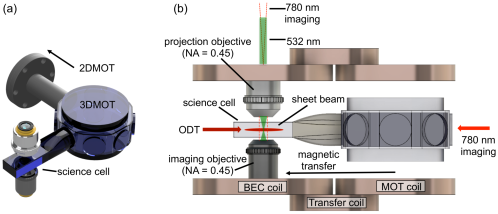
Our apparatus consists of a three-part vacuum system, comprising a two-dimensional magneto-optical trap (2DMOT), three-dimensional MOT (3DMOT) and attached science cell cuvette (see Fig. 1). The cell is made of Suprasil quartz and has 1.25 mm thick walls with an external broadband anti-reflection coating. The 2DMOT is separated from the 3DMOT and science cell sections with a 12 mm long differential pumping tube with a 1.2 mm inner diameter. This results in a pressure differential of , with a pressure of Torr and Torr on the 3DMOT and 2DMOT sides respectively. The 2DMOT loads 87Rb atoms into the 3DMOT in 5 s. The subsequent BEC production closely follows the methodology of Ref. lin2009rapid . After a 40 ms compressed MOT stage (CMOT) petrich1994behavior , the atoms are optically pumped to the manifold and captured in a 100 G/cm quadrupole magnetic field. Using two additional anti-Helmoltz coil pairs parry2014note (see Fig. 1), the atoms are adiabatically transferred to the science cell in s greiner2001magnetic . The quadrupole field is subsequently increased to 145 G/cm, and evaporation occurs over 4 s by driving the microwave transition from , resulting in a cloud of atoms at a temperature of K. The field is then relaxed to 27 G/cm, loading atoms at K into a red-detuned 1064 nm beam with a m waist, aligned m below the quadrupole zero, and with a potential depth of 110 . We find that the cancellation of stray magnetic fields is important for efficient loading of the dipole trap. Optical evaporation is performed by reducing the beam intensity, resulting in a temperature of nK, with a critical temperature for condensation of nK. If the optical evaporation is continued, BECs of atoms can be produced in this trap. Instead, we load the cold thermal atoms into a second 1064 nm red-detuned beam focused into a sheet with radial and vertical waists () = (1 mm, 8.5 m) and a trap depth of 6.4 . Subsequent evaporation in the sheet-magnetic hybrid trap results in a BEC of atoms in a highly flattened geometry, with final trapping frequencies of Hz. After evaporating in the sheet hybrid trap, we subsequently remove the magnetic field, while ramping up the sheet potential, resulting in all-optical confinement with Hz. The addition of the DMD potential to the sheet (see below) can dominate the weak radial harmonic confinement of this trap, producing nearly uniform atomic distributions.
III DMD projection
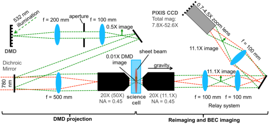
In order to produce arbitrarily patterned BECs, we directly image a DMD (Visitech LUXBEAM 4600 WUXGA 12001920 pixels) to the atom plane by illuminating the surface with spatially-filtered 532 nm light as shown in Fig. 2. This results in approximately Gaussian illumination with mm and maximum DMD diffraction efficiency of 40%. An intermediate image of the DMD with magnification is initially produced using a matched achromat imaging system. An aperture at the Fourier plane of this system removes spurious DMD diffraction orders, which otherwise contribute stray light to the dark regions of the imaged patterns and reduce the trap lifetime. Subsequently, the DMD is imaged to the atom plane using a 500 mm achromat and Nikon CFI L PLAN EPI 20XCR infinity corrected objective, resulting in magnification. The total system thus images the DMD to the atom plane with a final minimization factor of 100 ( magnification). The objective has a numerical aperture (NA) of 0.45 and an adjustable glass correction collar. We have found the correction collar to be important in obtaining high-resolution patterns inside the science cell, but the system is relatively insensitive to the precise angle of the objective and only requires coarse tuning.
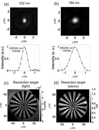
As the DMD mirrors have only two states — on and off — the resulting image is binary. However, given the limited spatial resolution of a typical optical system, the technique know as error-diffusion or halftoning can be used to produce intensity gradients liang20091 ; kumar2016minimally ; floyd1976adaptive . We determine the resolution of our system by first turning on a single mirror of the DMD and projecting it on to the atom plane. The mirror pitch is 10.8 m, so the minification factor of 100 results in an imaged mirror width of 108 nm, below the theoretical resolution limit of the top microscope system (605 nm FWHM at 532 nm illumination). As the single mirror is not resolvable, its image at the atom plane approximates the point-spread function (PSF) of the DMD imaging system. We reimage this focused spot on the camera with the bottom microscope system. Accounting for the magnification factor of the reimaging system results in a 650(50) nm FWHM peak in the atom plane, as shown in Fig. 3(a). This value is an upper limit, as it convolves any abberations of the reimaging system into the estimate of the spot size at the atom plane. Back-propagating this resolution element to the DMD location gives a 65 m spot which spans a block of mirrors; multiple mirrors will thus contribute to the resolution spot in the atom plane liang20091 . We therefore can use error-diffusion to control the light intensity at the atom plane, as shown in Fig. 4(b).
IV Atom trapping and imaging
The right half of Fig. 2 illustrates the bottom microscope imaging system. A second microscope objective (Olympus LCPLN20XIR) similar to the projection objective with a 0.45 NA and correction collar, but with near-infrared coatings, forms the first part of the imaging system. Collimated light at 780 nm is produced through the top objective, resulting in an imaging beam 1.1 mm in diameter. We then incorporate a lens relay system to allow us to implement dark-field imaging in the future wilson2015situ ; pappa2011ultra . Finally, an intermediate image is formed with magnification which is then reimaged to the CCD camera (PIXIS 1024B) with the adjustable VZM450 zoom lens ( – ). We therefore produce absorption images of the condensate in the final trap configurations with a total zoom of ( – ). By again turning on a single mirror of the DMD, but illuminating it at 780 nm, we can estimate the PSF at this wavelength, as shown in Fig. 3(b). This results in a 960(80) nm FWHM peak, consistent with the measurement at 532 nm after accounting for the increased wavelength.
The resulting high resolution DMD patterns produce a repulsive potential for the atoms trapped in the sheet-magnetic hybrid. We ramp on the intensity of the laser illuminating the DMD near the end of the final evaporation sequence in the sheet-hybrid trap to a value , where is the chemical potential of the BEC in the final trapping potential. In the case of a 80 m 50 m rectangular trapping geometry, the chemical potential calculated using the measured trap frequencies and 700,000 atoms is . Subsequently, the sheet power is linearly increased over 500 ms to keep the atoms trapped vertically while the magnetic field is linearly ramped to zero, increasing the vertical trapping frequency to Hz. The light power incident on the DMD can also be increased in this step. However, we have observed a decrease in the BEC lifetime with increasing intensity, with measured time constants of (18.2, 10.9, 9.1, 8.2) s for a 80 m 50 m rectangular DMD box potential with peaks of (1.2, 2.4, 4.8, 7.2) respectively. Similar intensity-dependent lifetimes were observed for different trap geometries. As the atoms are confined to areas of low DMD light intensity, we believe residual vibrational coupling in the DMD optical path results in parametric heating of the cloud.
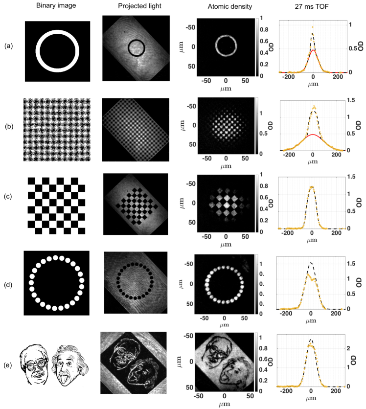
Several high-resolution atom-trap configurations are shown in Fig. 4, emphasizing the wide range of possible patterns. These are imaged immediately after turning off the optical trap. Alternatively, by imaging from the side after 27 ms time of flight (TOF) expansion, we can determine atom number and BEC fraction for the different distributions. We note that we have used the same evaporation ramp for each of these configurations — we expect that a near pure BEC can be achieved for each with optimization. We generally observe lower condensate fractions for smaller enclosed areas for similar optical evaporation profiles.
We briefly describe examples of the trapping potentials we have generated. Figure 4(a) demonstrates a ring trap, of interest for atom interferometry gupta2005bose and studies of phase slips and persistent currents eckel2014interferometric ; corman2014quench . Figure 4(b) shows a 10 m-period optical lattice. The binary DMD pattern was generated by applying a Floyd-Steinberg error diffusion algorithm floyd1976adaptive to an 8-bit grayscale image of a sinusoidal lattice. As we have not included a boundary to the lattice in the DMD pattern, we leave the magnetic field on and retain a Hz radial trapping frequency, producing a more symmetrically filled lattice. Figure 4(c) demonstrates a checkerboard pattern applied to the BEC, and the evaporation ramp in this case results in a BEC with negligible thermal component. This pattern emphasizes the sharp features in the atomic distribution resulting from the highly resolved features of the DMD pattern. Ring lattices have generated wide interest amico2005quantum , and Fig. 4(d) demonstrates a ring lattice of 25 sites. Finally, in Fig. 4(e) we project artistic impressions of Bose and Einstein into a nearly pure BEC, resulting in a ”Bose-Einstein” Bose-Einstein condensate and demonstrating our ability to create arbitrary potentials. This image is an average over 5 experimental runs (30 s experimental cycle) and is similar to Fig. 3(d) which uses a 10-run average. These images demonstrate the repeatability of the high-resolution patterned BECs. The integrated OD TOF cross sections in Fig. 4(d-e) deviate from Gaussian fit at their center. In the case of Fig. 4(d), this is due to uneven density distribution of atoms across the ring lattice and insufficient spatial overlap, or incoherent overlap of the lattice sites after only 27 ms TOF. In the case of Fig. 4(e), this deviation comes from to the high atomic densities leading to ODs above which are below the signal to noise threshold of the horizontal-imaging. In each of these cases, the limited expansion of the cloud, when compared with the thermal component of Fig. 4(b), along with the lack of a bimodal distribution, indicate a relatively pure BEC state.
V Measuring the modulation transfer function from light and atomic distributions
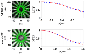
For a more quantitative characterisation of the optical systems horstmeyer2016standardizing , we produced a binary Siemens star resolution target on the DMD, imaged the projected light pattern, and imaged BECs loaded in to the pattern, as shown in Fig. 3(c,d). These patterns can then be analyzed to determine the modulation transfer function (MTF) of the total optical system. This is accomplished using the protocol illustrated in Fig. 5. We first determine circular paths around the Siemens star, with frequency spacings line-pairs (lp)/m, for the (light, atom) Siemens star. A contrast value is found for each of the 16 adjacent bright and dark spoke pairs, and the average contrast is calculated for each circular path. As the MTF is the Fourier transform of the PSF, which we estimate with a Gaussian fit, we extract a FWHM from a Gaussian fit of the measured MTF. These quantities are then related by , allowing us to compare the PSF FWHM extracted from the MTF with that of the single mirror image. For the Siemens star with 532 nm light, we find a MTF FWHM of lp/m, corresponding to a PSF FWHM of 630(10) nm, in agreement with the 650(50) nm measurement of the single mirror image. When imaging a BEC in the Siemens star pattern, we find a MTF FWHM of lp/m, corresponding to a PSF FWHM of 1250(20) nm, larger than the 960(80) nm single mirror image at 780 nm illumination. We believe that this increase is consistent with atom diffusion due to photon recoil during the 10 s repump and resonant imaging pulse muessel2013optimized .
VI Time-averaged potentials with DMDs
The DMD is capable of switching mirrors from DC to the specified maximum frequency of 20 kHz, which we have verified through photodiode measurement. This wide modulation range, along with the ability to store 13,889 frames on the device, enables a high level of dynamic control. At low modulation frequencies this allows adiabatic deformation of the DMD potentials. At the other extreme, high frequency switching can be utilised for quickly quenching the potential geometry. Furthermore, the painted-potentials technique is possible, where an average dipole force is produced through rapid modulation of the optical field schnelle2008versatile ; henderson2009experimental . This suggests pulse-width-modulation (PWM) as an alternative technique to error diffusion for producing grayscale levels, analogous to the techniques used in DLP.
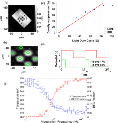
To explore the suitability of this system for producing time averaged potentials, we produced the DMD pattern shown in Fig. 6, consisting of an array of six 8 m diameter barriers contained in a 50 m 80 m rectangle. PWM, with the DMD running at an envelope frequency of kHz, was utilised, and the leading edge of each pulse was fixed. The hexagonal array within the rectangle was modulated with varying duty cycle over six levels by subdividing the carrier pulse into six modulation divisions, with the maximum duty cycle corresponding to all divisions turned on, and the minimum corresponding to one division turned on. The carrier frequency thus used was kHz. We illuminated the DMD with light corresponding to a trap depth of 1.2. The corresponding relative atomic densities are shown in Fig. 6(c).
To investigate the limits of this technique, we measured the effect on temperature and BEC fraction due to modulation of a single barrier (labeled ”3” in Fig. 6) which had a 50% duty cycle. After first forming the BEC in the rectangle in the absence of any internal barrier, we performed a modulation for 500 cycles at fixed frequencies ranging from 100 Hz to 16 kHz. We observed a decreasing effect as the frequencies are increased due to net energy gain per cycle decreasing since the barrier oscillates on a smaller time scale than atom diffusion timescales; above kHz the effect is negligible.
VII Conclusions
DMD devices combined with commercially-available glass-corrected objectives present a powerful technique for both the microscopic patterning of quantum gases and more general optical trapping. By utilising a commercial fluorescence cell with relatively thin 1.25 mm walls, expensive custom-built objectives can be avoided while still achieving high resolution. We are able to estimate a 630(10) nm FWHM PSF for our DMD projection system at 532 nm illumination, in agreement with the single-mirror analysis. A similar estimate of the PSF at 780 nm using a single mirror gives 960(80) nm FWHM, while MTF analysis of an atomic resolution target gives 1250(20) nm FWHM. We believe the broadening is due to diffusion of the atoms during the 10 s repump and resonant imaging pulses. We note that off-resonant imaging techniques such as darkground or Faraday imaging wilson2015situ ; pappa2011ultra might allow atomic distributions to be imaged with the full resolution.
Commercial DMD devices are now well-suited for implementation in both quantum gas experiments and other optical trapping applications. The painted-potentials technique, in combination with error diffusion methods, can generate grayscale potentials with more than one hundred levels. The ability to easily store and trigger 13,889 frames at high speed shows great promise for the dynamic control of these microscopic potentials. Furthermore, the ability to nearly instantaneously quench the potential geometry has many potential applications, such as investigations of superfluid transport between reservoirs lee2013analogs ; lee2015contact , and a demonstration of the superfluid fountain effect in BECs karpiuk2012superfluid . These techniques may prove useful in the production of superfluid turbulence in BECs, where, for example, the production and control of vortex pairs using moving potential barriers has recently been demonstrated samson2015deterministic ; tw2012experimental . Configurable trap geometries will be necessary for designing atomtronic circuits seaman2007atomtronics . As the DMD is largely wavelength insensitive (except in terms of diffraction efficiency), the possibilities for use at multiple wavelengths are intriguing. This capability could be utilised for the production of species dependent potentials catani2009entropy . Concurrent work by the Munich group has shown the usefulness of high resolution direct imaging (600 nm FWHM) of a DMD in creation of a two-dimensional disordered lattice for the exploration many body localization transitions Choi2016exploring .
More generally, our results demonstrate the utility of direct imaging of an DMD. With a well-corrected optical system, performance close to the diffraction limit can still be achieved at a non-trivial 0.45 NA. The computational simplicity of direct imaging may prove an advantage in applications that require reconfiguration in real-time; the high operating speed of the DMD furthermore facilitates this. These results are also applicable to optical trapping beyond quantum gases and in particular may be advantageous for the production of numerous traps for confining arrays of particles chowdhury2014automated ; eriksen2002multiple ; curtis2002dynamic .
Funding Information
Australian Research Council (ARC) (CE1101013, DP160102085).
Acknowledgments
We would like to acknowledge the contributions of Thomas Carey to the initial technical development of the BEC apparatus, and Alexander Stilgoe for useful discussions.
References
- (1) D. G. Grier, “A revolution in optical manipulation,” Nature 424, 810–816 (2003).
- (2) M. Woerdemann, C. Alpmann, M. Esseling, and C. Denz, “Advanced optical trapping by complex beam shaping,” Laser & Photonics Reviews 7, 839–854 (2013).
- (3) K. C. Neuman and S. M. Block, “Optical trapping,” Review of Scientific Instruments 75, 2787–2809 (2004).
- (4) S. Chowdhury, A. Thakur, P. Svec, C. Wang, W. Losert, and S. K. Gupta, “Automated manipulation of biological cells using gripper formations controlled by optical tweezers,” Automation Science and Engineering, IEEE Transactions on 11, 338–347 (2014).
- (5) M. Pasienski and B. DeMarco, “A high-accuracy algorithm for designing arbitrary holographic atom traps.” Optics Express 16, 2176–2190 (2008).
- (6) A. Gaunt and Z. Hadzibabic, “Robust digital holography for ultracold atom trapping.” Scientific Reports 2, 721–721 (2011).
- (7) T. Harte, G. D. Bruce, J. Keeling, and D. Cassettari, “Conjugate gradient minimisation approach to generating holographic traps for ultracold atoms,” Optics Express 22, 26548–26558 (2014).
- (8) F. Nogrette, H. Labuhn, S. Ravets, D. Barredo, L. Béguin, A. Vernier, T. Lahaye, and A. Browaeys, “Single-atom trapping in holographic 2D arrays of microtraps with arbitrary geometries,” Physical Review X 4, 021034 (2014).
- (9) P. M. Preiss, R. Ma, M. E. Tai, A. Lukin, M. Rispoli, P. Zupancic, Y. Lahini, R. Islam, and M. Greiner, “Strongly correlated quantum walks in optical lattices,” Science 347, 1229–1233 (2015).
- (10) T. Fukuhara, A. Kantian, M. Endres, M. Cheneau, P. Schauß, S. Hild, D. Bellem, U. Schollwöck, T. Giamarchi, C. Gross, I. Bloch, and S. Kuhr, “Quantum dynamics of a mobile spin impurity,” Nature Physics 9, 235–241 (2013).
- (11) P. Zupancic, P. M. Preiss, R. Ma, A. Lukin, M. E. Tai, M. Rispoli, R. Islam, and M. Greiner, “Ultra-precise holographic beam shaping for microscopic quantum control,” arXiv preprint arXiv:1604.07653 (2016).
- (12) N. M. Parry, M. Baker, T. Neely, T. Carey, T. Bell, and H. Rubinsztein-Dunlop, “Note: High turn density magnetic coils with improved low pressure water cooling for use in atom optics,” Review of Scientific Instruments 85, 086103 (2014).
- (13) P. C. Mogensen and J. Glückstad, “Dynamic array generation and pattern formation for optical tweezers,” Optics Communications 175, 75–81 (2000).
- (14) R. L. Eriksen, P. C. Mogensen, and J. Glückstad, “Multiple-beam optical tweezers generated by the generalized phase-contrast method,” Optics Letters 27, 267–269 (2002).
- (15) J. E. Curtis, B. A. Koss, and D. G. Grier, “Dynamic holographic optical tweezers,” Optics Communications 207, 169–175 (2002).
- (16) D. Dudley, W. M. Duncan, and J. Slaughter, “Emerging digital micromirror device (DMD) applications,” (2003).
- (17) J. Liang, R. N. Kohn Jr, M. F. Becker, and D. J. Heinzen, “1.5% root-mean-square flat-intensity laser beam formed using a binary-amplitude spatial light modulator,” Applied Optics 48, 1955–1962 (2009).
- (18) L.-C. Ha, L. W. Clark, C. V. Parker, B. M. Anderson, and C. Chin, “Roton-maxon excitation spectrum of Bose condensates in a shaken optical lattice,” Physical Review Letters 114, 055301 (2015).
- (19) A. Kumar, N. Anderson, W. Phillips, S. Eckel, G. Campbell, and S. Stringari, “Minimally destructive, Doppler measurement of a quantized flow in a ring-shaped Bose-Einstein condensate,” New Journal of Physics 18, 025001 (2016).
- (20) A. B. Stilgoe, A. V. Kashchuk, D. Preece, and H. Rubinsztein-Dunlop, “An interpretation and guide to single-pass beam shaping methods using SLMs and DMDs,” Journal of Optics 18, 065609 (2016).
- (21) M. Mirhosseini, O. S. Magana-Loaiza, C. Chen, B. Rodenburg, M. Malik, and R. W. Boyd, “Rapid generation of light beams carrying orbital angular momentum,” Optics Express 21, 30196–30203 (2013).
- (22) R. Liu, F. Li, M. Padgett, and D. Phillips, “Generalized photon sieves: fine control of complex fields with simple pinhole arrays,” Optica 2, 1028–1036 (2015).
- (23) Our results represent an improvement over previously reported work on optical trapping of BECs using DMDs. We note that Ref. fukuhara2013quantum directly imaged a DMD with a higher resolution ( nm at 787.65 nm illumination) for the purposes of optical addressing of atoms trapped in an optical lattice, but not for atom trapping.
- (24) B. Zimmermann, T. Mueller, J. Meineke, T. Esslinger, and H. Moritz, “High-resolution imaging of ultracold fermions in microscopically tailored optical potentials,” New Journal of Physics 13, 043007 (2011).
- (25) S. Schnelle, E. Van Ooijen, M. Davis, N. Heckenberg, and H. Rubinsztein-Dunlop, “Versatile two-dimensional potentials for ultra-cold atoms,” Optics Express 16, 1405–1412 (2008).
- (26) K. Henderson, C. Ryu, C. MacCormick, and M. Boshier, “Experimental demonstration of painting arbitrary and dynamic potentials for Bose-Einstein condensates,” New Journal of Physics 11, 043030 (2009).
- (27) T. A. Bell, J. A. P. Glidden, L. Humbert, M. W. J. Bromley, S. A. Haine, M. J. Davis, T. W. Neely, M. A. Baker, and H. Rubinsztein-Dunlop, “Bose-Einstein condensation in large time-averaged optical ring potentials,” New Journal of Physics 18, 035003 (2016).
- (28) Y.-J. Lin, A. Perry, R. Compton, I. Spielman, and J. Porto, “Rapid production of 87Rb Bose-Einstein condensates in a combined magnetic and optical potential,” Physical Review A 79, 063631 (2009).
- (29) W. Petrich, M. H. Anderson, J. R. Ensher, and E. A. Cornell, “Behavior of atoms in a compressed magneto-optical trap,” Journal of the Optical Society of America B 11, 1332–1335 (1994).
- (30) K. E. Wilson, Z. L. Newman, J. D. Lowney, and B. P. Anderson, “In situ imaging of vortices in Bose-Einstein condensates,” Physical Review A 91, 023621 (2015).
- (31) M. Pappa, P. Condylis, G. Konstantinidis, V. Bolpasi, A. Lazoudis, O. Morizot, D. Sahagun, M. Baker, and W. Von Klitzing, “Ultra-sensitive atom imaging for matter-wave optics,” New Journal of Physics 13, 115012 (2011).
- (32) M. Greiner, I. Bloch, T. W. Hänsch, and T. Esslinger, “Magnetic transport of trapped cold atoms over a large distance,” Physical Review A 63, 031401 (2001).
- (33) R. W. Floyd, “An adaptive algorithm for spatial gray-scale,” (1976).
- (34) S. Gupta, K. Murch, K. Moore, T. Purdy, and D. Stamper-Kurn, “Bose-Einstein condensation in a circular waveguide,” Physical Review Letters 95, 143201 (2005).
- (35) S. Eckel, F. Jendrzejewski, A. Kumar, C. Lobb, and G. Campbell, “Interferometric measurement of the current-phase relationship of a superfluid weak link,” Physical Review X 4, 031052 (2014).
- (36) L. Corman, L. Chomaz, T. Bienaimé, R. Desbuquois, C. Weitenberg, S. Nascimbene, J. Dalibard, and J. Beugnon, “Quench-induced supercurrents in an annular Bose gas,” Physical Review Letters 113, 135302 (2014).
- (37) L. Amico, A. Osterloh, and F. Cataliotti, “Quantum many particle systems in ring-shaped optical lattices,” Physical Review Letters 95, 063201 (2005).
- (38) R. Horstmeyer, R. Heintzmann, G. Popescu, L. Waller, and C. Yang, “Standardizing the resolution claims for coherent microscopy,” Nature Photonics 10, 68–71 (2016).
- (39) L. Mathey, A. Ramantahn, K. C. Wright, S. R. Muniz, W. D. Phillips, and W. Charles, “Phase fluctuations in anisotropic Bose-Einstein condensates: From cigars to rings,” Physical Review A 82, 033607 (2010).
- (40) Einstein image from www.muraldecal.com, used with permission.
- (41) W. Muessel, H. Strobel, M. Joos, E. Nicklas, I. Stroescu, J. Tomkovič, D. B. Hume, and M. K. Oberthaler, “Optimized absorption imaging of mesoscopic atomic clouds,” Applied Physics B 113, 69–73 (2013).
- (42) J. G. Lee, B. J. McIlvain, C. Lobb, and W. Hill III, “Analogs of basic electronic circuit elements in a free-space atom chip,” Scientific Reports 3 (2013).
- (43) J. Lee, S. Eckel, F. Jendrezjewski, C. Lobb, G. Campbell, and W. Hill III, “Contact resistance and phase slips in mesoscopic superfluid atom transport,” arXiv preprint arXiv:1506.08413 (2015).
- (44) T. Karpiuk, B. Gremaud, C. Miniatura, and M. Gajda, “Superfluid fountain effect in a Bose-Einstein condensate,” Physical Review A 86, 033619 (2012).
- (45) E. Samson, K. Wilson, Z. Newman, and B. Anderson, “Deterministic creation, pinning, and manipulation of quantized vortices in a Bose-Einstein condensate,” arXiv preprint arXiv:1508.05110 (2015).
- (46) K. E. Wilson, E. C. Samson, Z. L. Newman, T. W. Neely, and B. P. Anderson, “Experimental methods for generating two-dimensional quantum turbulence in Bose-Einstein condensates,” Annual Review of Cold Atoms and Molecules 1, 261 (2012).
- (47) B. Seaman, M. Krämer, D. Anderson, and M. Holland, “Atomtronics: Ultracold-atom analogs of electronic devices,” Physical Review A 75, 023615 (2007).
- (48) J. Catani, G. Barontini, G. Lamporesi, F. Rabatti, G. Thalhammer, F. Minardi, S. Stringari, and M. Inguscio, “Entropy exchange in a mixture of ultracold atoms,” Physical Review Letters 103, 140401 (2009).
- (49) J.-Y. Choi, S. Hild, J. Zeiher, P. Schauß, A. Rubio-Abadal, T. Yefsah, V. Khemani, D. A. Huse, I. Bloch, and C. Gross, “Exploring the many-body localization in two dimensions,” Science 352, 1547 (2016).