Nonlinear photocurrents in two-dimensional systems based on graphene and boron nitride
Abstract
The dc photoelectrical currents can be generated purely as a non-linear effect in uniform media lacking inversion symmetry without the need for a material junction or bias voltages to drive it, in what is termed photogalvanic effect. These currents are strongly dependent on the polarization state of the radiation, as well as on topological properties of the underlying Fermi surface such as its Berry curvature. In order to study the intrinsic photogalvanic response of gapped graphene, biased bilayer graphene (BBG), and hexagonal boron nitride (hBN), we compute the non-linear current using a perturbative expansion of the density matrix. This allows a microscopic description of the quadratic response to an electromagnetic field in these materials, which we analyze as a function of temperature and electron density. We find that the intrinsic response is robust across these systems and allows for currents in the range of pA cm/W to nA cm/W. At the independent-particle level, the response of hBN-based structures is significant only in the ultra-violet due to their sizable band-gap. However, when Coulomb interactions are accounted for by explicit solution of the Bethe-Salpeter equation, we find that the photoconductivity is strongly modified by transitions involving exciton levels in the gap region, whose spectral weight dominates in the overall frequency range. Biased bilayers and gapped monolayers of graphene have a strong photoconductivity in the visible and infrared window, allowing for photocurrent densities of several nA cm/W. We further show that the richer electronic dispersion of BBG at low energies and the ability to change its band-gap on demand allows a higher tunability of the photocurrent, including not only its magnitude but also, and significantly, its polarity.
pacs:
78.67.-n,78.67.Wj,81.05.ue,42.65.AnI Introduction
Non-linear photocurrents consist of dc electric currents induced in a material by non-linear interaction with an external electromagnetic field. This is frequently termed photogalvanic, or optical rectification effect Bass et al. (1962); Ivchenko (2005). It belongs to a vast class of processes arising from the non-linear response of matter to light fields, such as higher harmonic generation, sum/difference frequency generation, optical rectification, parametric oscillation, two-photon absorption, or stimulated Raman scattering. These processes have a broad range of applications, from non-linear optical microscopy, optical switching, tunable high-frequency lasers, surface analysis with non-linear optics, to parametric down conversion for generation of entangled photons Ghosh and Mandel (1987); Shih and Alley (1988); Boyd (2008); Shen (2002) and photocurrents Bass et al. (1962); Shen (2002). The photogalvanic effect is particularly interesting for optoelectronic applications as it opens the door for light-induced injection and steering of electric or spin currents Ivchenko (2005) without electrical contacts or the need of electric fields to separate photo-excited electron-hole pairs, as commonly happens in most applications of photo-generated currents.
In metallic structures, the non-linear response to external fields is frequently dominated by surface states as a result of the large absorption in metals. This is both interesting and convenient in bulk crystals with inversion symmetry because elastic even-order interactions with electromagnetic fields are suppressed by symmetry in the bulk, but might be possible at the surface where the inversion symmetry is brokenBoyd (2008); Haussühl (2007).
The wealth of strictly two-dimensional systems that emerged in the wake of the success of graphene, with a range of different intrinsic opto-electronic properties that continues to grow, provide a particularly fertile setting to explore non-linear optical properties. Two of their important characteristics in this context are the intrinsically low absorption as light traverses only one or a few atomic layers, and the ease to fabricate planar heterostructures based on combining different functionalities that are important for photoelectric and photogalvanic devices. Moreover, in many of them the electronic density and/or gap can be tuned externally by field effect Zhang et al. (2009); Castro et al. (2007) or electrolytic gating Das et al. (2008), thereby allowing control over two key parameters that determine the optical response.
In this paper, we analyze the characteristics of the second-order electrical conductivity tensor with a focus on the intrinsic photoconductivity of graphene-based systems and boron-nitride using a perturbative expansion of the density matrix. We start with a brief analysis of symmetry, followed by an overview of the formalism proposed in Ref. Aversa and Sipe, 1995 to compute the relevant response functions. In the main sections, we analyze in detail the features of the photoconductivity in monolayers of “gapped graphene”, of which the canonical example is hBN (hexagonal boron nitride), as well as their bilayer counterparts which can display a richer response when the inter-layer bias and chemical potential are independently controlled. The photogalvanic reponse is a second order non-linear effect and, therefore, requires broken inversion symmetry in the dipole limit. We systematically investigate the influence of stacking sequence on the inversion symmetry of various bilayer structures. It has previously been established that the second order non-linear optical response, in the form of second harmonic generation, in bilayer graphene is very large Brun and Pedersen (2015). Moreover, the response is highly tunable by external gating or variations in doping level. We find that similar conclusions hold for the photogalvanic response.
In the last section we address the role of excitons in the photoconductivity of these two-dimensional insulators, and establish that, similarly to the large renormalization that they cause in the linear optical conductivity, the excitonic response is crucial for an accurate characterization of the quadratic response. The important role of excitons in second harmonic generation from two-dimensional materials has previously been demonstrated for MoS2 and hBNTrolle et al. (2014); Pedersen (2015). Hence, in the last part of this paper, we apply the excitonic intraband formalism developed in Ref. Pedersen, 2015 to include Coulomb interactions in the non-linear photoconductivity of hBN. In this manner, we show that excitons lead to a large red-shift of the response as well as a renormalization of the spectrum above the band gap.
II Symmetry considerations
The essence of response theory applied to photocurrent generation is that, when an electromagnetic wave with electric field
| (1) |
impinges on an electronic system, the induced current density can be, quite generically, expressed as a sum of contributions proportional to increasing powers of the field magnitude,
| (2) |
This defines the -th order frequency-dependent conductivity, a tensor of rank that determines the Cartesian component of the current, , as a function of time. A perennial question in this context is to determine at a given order from the microscopic details of the target system (symmetry, electronic structure, interactions, etc.).
The dc photocurrent arising in the intrinsic photogalvanic effect results from the existence of a non-zero quadratic response in systems that fulfill certain symmetry criteria. Foremost is the fact that, being an odd-rank tensor, it can only be sustained in the absence of inversion symmetry. In addition to this, the most basic threefold symmetry common to all honeycomb-based lattices considerably reduces the non-zero independent components of . Under the point group symmetry, we have only two independent in-plane components, say and , as well as the constraints , . In Table 1, we identify the symmetry and non-vanishing components of rank-3 tensors for mono and bilayers of graphene and hBN that are appropriate for the target systems in this paper. It contains the relevant space (SG) and point groups (PG) for the lattices under consideration and highlights the presence or absence of inversion symmetry in each case Dresselhaus et al. (2008); Haussühl (2007).
| material | stacking | SG | PG | i | |
| graphene | SL | yes | none | ||
| AB | yes | none | |||
| (biased) | AB | no | |||
| hBN | SL | no | |||
| AA | no | ||||
| AA’ | yes | none | |||
| AB | no | ||||
| A’B | yes | none | |||
| AB’ | yes | none |
Among the cases selected to analyze in detail here, the restrictions imposed by lattice symmetry are most stringent in graphene, where both free standing monolayer and AB bilayers have inversion symmetry. However, second order response is possible in biased AB graphene bilayers because the potential difference between the two layers naturally breaks that symmetryBrun and Pedersen (2015). In contrast, due to the presence of two distinct elements in the unit cell, an hBN monolayer does not have an inversion center and, consequently, its quadratic response can be finite. In addition, the stacking order plays an important role in hBN bilayers since a majority of possible stackings results in inversion-symmetric lattices (namely, AA’, A’B, and AB’). In the remainder of this paper we will compute and analyze the intrinsic photoconductivity of the systems listed in the table whose response is not suppressed by symmetry.
III Calculation of non-linear response functions
We shall be interested in the interaction of the electronic system in a crystal with light, for which we can neglect the position dependence of the electromagnetic field in a first (dipole) approximation, and write the total Hamiltonian of the system as
| (3) |
Here, represents the Hamiltonian of the electrons in the periodic crystal and the explicitly time-dependent external field and is the elementary charge. The field is taken to be monochromatic and parametrized as in Eq. 1. The eigenvalues of the unperturbed Hamiltonian define the band energies , and its eigenstates, , are the corresponding Bloch waves. In the derivations below, electronic interactions are neglected and, hence, collective effects arise simply on account of the Fermi-Dirac statistics. In the last section, however, we investigate the effect of Coulomb interactions on the excited electronic states, i.e. excitons. These effects are studied only for the simple case of monolayer hBN, though.
III.1 Perturbative expansion of the density matrix
The time evolution of a system governed by the Hamiltonian (3) is entirely determined if one computes the time-dependent density operator
| (4) |
that obeys the dynamical (quantum Liouville) equation or, more explicitly,
| (5) |
Knowledge of permits one to readily quantify and characterize the electric current density in terms of the polarization and intensity of the field . The current density is given in terms of the single-particle velocity operator,
| (6) |
by
| (7) |
where accounts for the spin degeneracy and is the -dimensional volume of the system.
The formal integration of (5) is facilitated in the interaction picture with respect to the external perturbation, and leads to the conventional perturbative expansion of the density operator in powers of the perturbation Sakurai (1967). In a crystal, however, such straightforward expansion cannot be directly used for the perturbation defined in (3) because it involves matrix elements of the position between Bloch states such as , which are notably ill defined Blount (1962). The integration of Eq. 5 thus requires a more careful treatment of these matrix elements. Moreover, the potential alternative of effecting a gauge transformation to describe the external field in the minimal coupling scheme is plagued by its own difficulties in the non-linear response functions it generates, most notably the appearance of non-physical divergences in the dc limit of an insulator at zero temperature Moss et al. (1990). To navigate these difficulties, we follow the systematic approach proposed in Ref. Aversa and Sipe, 1995 to handle the external field perturbation as expressed in equation (3). In order to provide here a self-contained account of our calculations we briefly review the key aspects of that approach.
An important step is to express matrix elements of the position operator between Bloch states as Blount (1962)
| (8) |
where is the so-called Berry connection Berry (1984); Xiao et al. (2010); Aversa and Sipe (1995) and
| (9) |
is the Kronecker delta with representing the volume of the unit cell. We normalize the Bloch states in the finite volume as
| (10) |
with a cell-periodic function. The Berry connection then has the explicit form
| (11) |
For brevity, we will frequently omit the explicit dependence in , and other quantities when there is no risk of confusion. Equation (8) suggests a natural identification of two types of matrix elements, interband and intraband, respectively given by
| (12a) | ||||
| (12b) | ||||
In this expression, is the usual Kronecker delta, and . This allows a decomposition of the position operator into a purely interband component and another purely intraband, , with
| (13) | ||||
| (14) |
With these definitions, Eq. 5 can be recast as Aversa and Sipe (1995)
| (15) |
where and the second term contains the generalized (gauge invariant) gradient Aversa and Sipe (1995)
| (16) |
The purpose of writing Eq. 5 as (15) is that, now, all the matrix elements appearing in (15) are well defined and non-singular, which would not be the case if we had generated an equivalent expansion in terms of matrix elements directly from (5).
Equation (15) can be straightforwardly integrated recursively yielding a series in increasing powers of the electric field,
| (17) |
Each term is associated with the -th order response function. Since we are ultimately interested in the electrical currents induced by the external radiation field, we will compute the non-linear conductivity which is the natural response function for this case. In the absence of the light field, the system is in equilibrium and its effective single-particle density matrix reduces to , a simple Fermi-Dirac distribution. This unperturbed density matrix begins the iterative solution of Eq. 15 which is then straightforward and we obtain, in first order in the electric field,
| (18a) | ||||
| where we introduced , , and the frequency summation should be interpreted as including the two possible Fourier components, i.e. . Also, with a positive infinitesimal is added to each frequency to ensure adiabatic turn-on of the field. However, to improve numerical stability and account for broadening in realistic spectra, we will keep finite but small throughout. In addition, in (18a) and henceforth, Greek superscripts denote Cartesian components and are implicitly summed over when they appear repeated. The second-order contribution to the density matrix reads as | ||||
| (18b) | ||||
where the generalized derivative introduced in Eq. 16 appears explicitly in the last term.
III.2 Linear and quadratic response functions
The current response at any desired order is obtained by substituting the perturbative expansion (17) in equation (7),
| (19) |
where
| (20) |
According to the earlier definition in equation (2),
| (21) |
which defines the -th order optical conductivity . In this expression, means a summation that runs over all , and each takes all the values that define the harmonic content of the external field. In the case of a single source of monochromatic light as in (1), we have simply . Equation (21) transparently shows that, in quadratic and higher orders, the time dependence of the response is richer than that of the external field, with the characteristic appearance of up to higher order harmonics of the input frequency. In particular, in second order we see that it is possible to induce a dc contribution (constant in time) to that is determined by . This particular response function — the photoconductivity — is our main focus in this paper.
As a preliminary illustration, one obtains the linear optical conductivity by directly combining the results in Eq. 18 with the definitions above:
| (22) |
with , , and . We have written explicitly in terms of the matrix elements of the velocity operator using the relation that follows from Eqs. (6 and 12) when . Note that, in this form, the two terms that make up the result above directly, and individually, reflect the interband () and intraband () contributions to the overall optical conductivity. For example, the Drude component can be read from the first term in (III.2) due to the constraint . In fact, one can readily see that
| (23) |
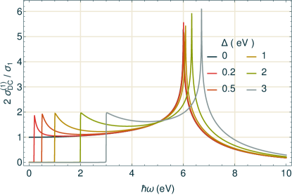
where the Drude weight is , is the density of states (DOS) at the Fermi level, and denotes an average over the Fermi surface Gusynin and Sharapov (2006). This component is zero in the presence of a band gap for a clean system (as happens in most of the situations we consider throughout this paper) as long as the chemical potential remains in the gapped region and the temperature is low. In such cases, that include the peculiar situation of undoped graphene, the linear conductivity is uniquely determined by the interband component Peres et al. (2006); Gusynin and Sharapov (2006); Stauber et al. (2008a); Mak et al. (2008). Several examples are shown in Fig. 1.
The clear distinction between inter and intraband terms in the final expressions for the conductivity is a direct result of the earlier decomposition of the position matrix elements (12), and propagates to higher orders Aversa and Sipe (1995). In particular, the quadratic conductivity can be decomposed into four distinct contributions:
| (24) |
where
| (25a) | ||||
| (25b) | ||||
| (25c) | ||||
| (25d) | ||||
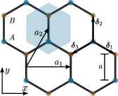
In these expressions, refers to a contribution including interband matrix elements only, to that including purely intraband, and , to those that include one inter and one intraband matrix element. For later convenience, the constant is defined in terms of the in-plane nearest-neighbor lattice parameter and hopping integral (cf. Fig. 2).

The results (24) completely describe the quadratic response of the system for any combination of the pair of frequencies and . Henceforth, we shall be interested only in the specific case of that characterizes the intrinsic photoconductivity of the system: how much current density is driven in the system for a given intensity and polarization of the incident electromagnetic radiation. This response function is associated with the effect known as photoconductivity. To ease the notation, we define
| (26) |
where the subscript “dc” emphasizes that the induced current is constant in time. Since there is no risk of ambiguity and, moreover, a system with point group symmetry has only one independent tensor component, will be used from this point on.
IV Photoconductivity of monolayer honeycomb lattices
To actually compute the linear and quadratic conductivities in Eq. III.2 or 24, we must determine not only the electronic energy bands, but also the matrix elements of the velocity, , and Berry connection, , involving any two bands. A simple one orbital tight-binding (TB) model provides an accurate, yet simple, description of such quantities in graphene and boron nitride (monolayers and bilayers).
Consider the general case of a single layer of a honeycomb lattice where the atoms residing in the A and B sublattices can be different, a canonical example being a monolayer of hBN. The direct and reciprocal lattices of such a crystal are illustrated in Fig. 2. In a single orbital, nearest neighbor tight-binding modeling of the relevant electronic degrees of freedom, the Hamiltonian operator takes the form
| (27) |
where comprises the Fourier-transformed electron creation operators at sites of the A and B sublattices, and is the reduced Hamiltonian in the crystal momentum representation:
| (28) |
Henceforth, we use units of energy such that . Here, quantifies the difference in the atomic energy of A- and B-type atoms, and , being the nearest neighbor distance. This description yields the simple two-band energy dispersion
| (29) |
In this tight-binding parametrization, the velocity matrix elements and Berry connection (28) are simply
| (30) |
where are the normalized eigenstates of (28).
IV.1 Hexagonal boron nitride
A system to which the Hamiltonian above is directly relevant is that of a monolayer of boron nitride, whose crystal lattice consists of a honeycomb structure where the B and N atoms occupy distinct sublattices. We follow the parametrization of Ref. Pedersen, 2015 for the hopping and gap, namely , , and the nearest neighbor distance is .
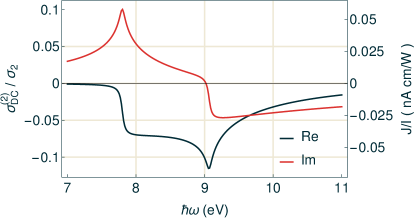
The symmetry constraints greatly facilitate the calculation of the quadratic conductivity because, as only needs to be computed explicitly, the last two contributions (25c) and (25d) vanish identically as long as time-reversal symmetry is preserved. Hence, quite generically only and need to be computed in a system with threefold plane rotational symmetry. Moreover, in any two-band model, is also identically zero for the same reason.
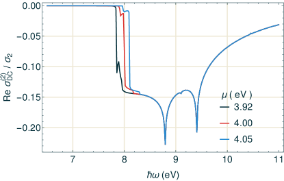
Figure 3(a) shows the real and imaginary parts of for a hBN monolayer computed directly from the results in eqs. (24). As anticipated from the nature of the frequency denominators in those expressions, the system mainly responds for photon energies at, or above, the band gap. The peak at eV is associated with virtual transitions between the van Hove singularities at the point in the Brillouin zone.
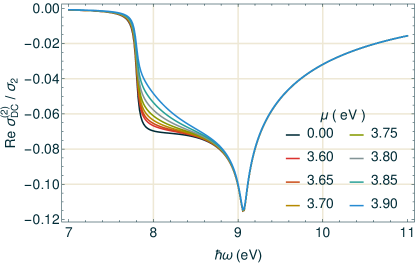
Unlike other two-dimensional (2D) crystals such as graphene or transition-metal dichalcogenides, the large gap in hBN makes it impossible to change the Fermi level by electrostatic gating. On the other hand, a small amount of impurities might introduce a shallow donor (acceptor) band and allow the chemical potential to be driven close to the edge of the conduction (valence) band. This scenario is explored in Fig. 3(b), where we show the effect of varying the chemical potential in the vicinity of the band edge at high temperature. High temperature is chosen here because the interaction with very intense laser light, as required to observe non-linear effects, generates hot carriers in the material. Experiments Sun et al. (2008); Ruzicka et al. (2010a, b); Lui et al. (2010); Sun et al. (2012); Tielrooij et al. (2013) in graphene indicate hot carrier temperatures in the range 1000 to 3600 K.
IV.2 Gapped graphene
The case of hBN can be seen as an extreme limit of “gapped graphene” in the framework of the effective two-band tight-binding model introduced in (28). We use the designation “gapped graphene” to describe a nearest-neighbor tight-binding model like that of graphene, but where the sublattice symmetry is explicitly broken by introducing a potential energy that differs by an amount between the two sublattices [see (28)]. Second order non-linearities are not expected in pristine graphene, or any odd numbered Bernal stacked multi-layers due to the presence of an inversion center Jorio et al. (2011). Breaking the sublattice symmetry in a monolayer, in addition to opening a band-gap, lifts this restriction. It is of general interest to describe and understand the behavior of the photoconductivity as a function of gap magnitude in such a system: on the one hand, such sublattice symmetry breaking has been predicted to take place when graphene is grown or transferred to particular substrates Giovannetti et al. (2007); Zhou et al. (2007); Sławińska et al. (2010); Dean et al. (2010); Ortix et al. (2012); Chen et al. (2014); Bokdam et al. (2014); Woods et al. (2014); Yankowitz et al. (2014); Huang et al. (2014); on the other hand, models such as (28) are frequently used as minimal descriptions of the low-energy details in many transition metal dichalcogenides. We note that inversion symmetry in graphene can also be broken by rolling the material into chiral nanotubes Pedersen and Pedersen (2009), for which the gapped graphene model may also be applied.
Using the parameters relevant for graphene to be definite, we computed explicitly the four non-vanishing elements of the photoconductivity tensor , which are shown in Fig. 4 when the gap . That the curves for distinct components coincide and cannot be distinguished in the figure documents a correct implementation of our computation of the various terms in (24).
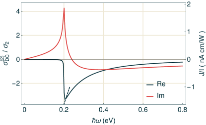
The real part of should share key features of the joint density of states for transitions between the valence and conduction bands. In particular, it should display an onset of response at precisely (for ), and van Hove singularities at frequencies coinciding with transitions between locally flat portions of the band dispersion. The band-gap feature can be clearly identified in the figure. Note, however, an important difference in contrast to the case shown in Fig. 3 for an actual realization of hBN: for small gap, the response is much stronger at frequencies in the vicinity of the gap (compare the magnitude of at in the two cases). Since the low frequency features are governed by the nature of virtual transitions in the vicinity of the point of the Brillouin zone (BZ), we can understand this behavior from an exact analytical standpoint which is possible to establish after expanding (24) in the vicinity of :
| (31) |
This curve that defines the onset of photoconductivity at is shown in Figs. 4 and Fig. 5(a) as dashed lines.
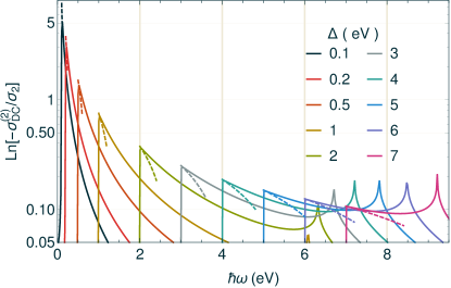
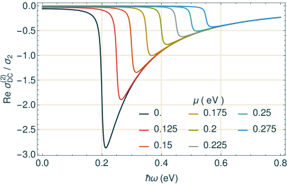
It is clear that the singular behavior at should be more prominent the smaller the gap. Since the magnitude of there is exactly , the frequencies near the optical absorption edge will entirely dominate the photoconductivity response for gaps smaller than eV. This is shown explicitly in Fig. 5(a), where we plot the photoconductivity for different gaps at very low temperature. The effect of varying the chemical potential is studied in Fig. 5(b) for representative cases. Since all the virtual transitions that define the response in a translationally invariant system are vertical (i.e., conserving the crystal momentum ), at a chemical potential in the conduction band will block any response for due to Pauli exclusion, as seen in the figure.
V Photoconductivity of bilayer honeycomb lattices
V.1 Biased bilayer graphene
If it is not clear within the current experimental landscape whether a realization of small gapped graphene is a realistic prospect, the existence of a band-gap in biased bilayer graphene (BBG) is a well-established experimental fact Zhang et al. (2009). Crucially, its gap is a function of the externally driven inter-layer bias voltage and, hence, tuneable Castro et al. (2007); Zhang et al. (2009). From this perspective, a BBG is a more natural candidate to explore the quadratic response to light.
A minimal tight-binding model that captures the electronic structure of Bernal-stacked bilayer graphene in the presence of a uniform electric field perpendicular to the plane, is given by Castro et al. (2007); McCann and Fal’ko (2006)
| (32) |
where represents the interlayer hopping and the difference in potential energy in the two layers induced by the external field. The dispersion function is the same that appears in Eq. 29. The Hamiltonian (32) is represented in the basis .
The largest gaps obtained by field effect with top and bottom-gated devices have not so far exceeded 0.5 eV Castro et al. (2007); Szafranek et al. (2011); Velasco et al. (2012); Pachoud et al. (2010); Britnell et al. (2012); Stabile et al. (2015). Hence, to be specific, we shall analyze the photocurrent in BBG with in the parametrization of (24).
The band structure of BBG can accommodate different types of vertical transitions in the low energy regime, thereby increasing the richness of the interaction with light. Having now one pair of conduction and another of valence bands means that transitions such as or become important at low frequencies because the separation between these bands (set by the interlayer hopping ) can easily be comparable to the bias-induced band-gap. What is more, chemical potential and bias (hence gap) can be controlled independently in experiments, allowing for a selective suppression of different types of transitions.
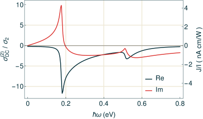
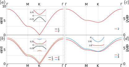
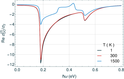
Figure 6 shows the intrinsic photoconductivity expected in charge-neutral BBG. At low temperature, the response exhibits two key features associated with the onset of the virtual transitions and (see Fig. 7 for details of the band labeling). As expected, no features appear related to transitions involving bands or due to Pauli blocking.
V.2 Finite temperatures, doping and broadening
If the temperature is high enough, we can see in Fig. 88 that the frequency response becomes much richer, and can even change sign in the range that is dictated by the magnitude of the inter-layer hopping . This is caused by the suppression of Pauli blocking with increasing temperature, leading to the emergence of spectral features associated with transitions from the bands and that are not effectively possible at room temperature. It is easy to conceive a direct application of this characteristic: since experiments that probe the non-linear response must be frequently done under relatively high power, the observation of spectral features expected to be Pauli blocked could be used as an indirect thermometer to estimate the local temperature of the electron gas in the system under illumination.
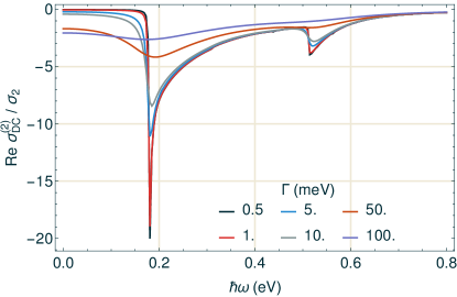
Since in this paper we are concerned with the generation of a dc electrical current through optical means, it is natural to wonder what effect the scattering of charge carriers by impurities might have in the strength and nature of the photocurrents. Although we do not explicitly include disorder in our calculations, and to the best of our knowledge, disorder has not been addressed in microscopic calculations of the non-linear optical response, we can draw insight from the effects that weak disorder has in the linear optical conductivity. In this context, several types of disorder have been studied and, in addition to the fact that dilute scatterers lead to perturbations proportional to their concentration, the leading qualitative effect of both short-ranged and Coulomb impurities is the broadening/smearing of the line shape characteristic of the pristine crystalsPeres et al. (2008); Stauber et al. (2008b); Stauber and Peres (2008); Abergel et al. (2012); Yuan et al. (2011). Correspondingly, we expect the main effect of weak disorder in the non-linear response to be captured qualitatively by making the adiabatic parameter in our calculations explicitly finite, with a magnitude that reflects a phenomenological scattering rate. That would be equivalent to assuming that self-energy corrections arising from disorder are featureless in momentum and frequency, which is a reasonable approximation for these cases. As an illustration, in Fig. 88, we study the sensitivity of the photocurrent to that scattering rate for the BBG at room temperature. The main features remain identifiable up to meV.
Notwithstanding the impact that disorder might have in the dc currents generated by the photogalvanic effect, the continuous progress in the production of high quality samples, such as encapsulating graphene between hBN crystals Gannett et al. (2011); Chari et al. (2015); Banszerus et al. (2016); Ni et al. (2016) and other techniques Pallecchi et al. (2014), has delivered procedures to achieve graphene-based electronic devices of progressively higher mobility and mean free paths up to Banszerus et al. (2016). This corresponds to a typical lifetime for ballistic transport of ps or a scattering rate meV. According to the data in Fig. 88, this means that, even though effects such as photon drag might compete with the photogalvanic effect at the quadratic order, it is not unrealistic to anticipate a class of systems where contributions to the photocurrent arising from impurity-assisted processes are minimal, and it is mostly determined by the intrinsic photogalvanic effect discussed here.
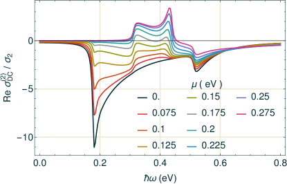
Finally, the results presented in Fig. 88 at different demonstrate that the ability to experimentally vary the chemical potential on demand through simple gating might allow external control over the polarity of the induced photocurrents within target frequency ranges. The sign of directly translates into the sign of the dc current in the material and, as we can see in this figure, the photocurrent can be made to switch from positive to negative at frequencies that are controlled by .
V.3 Bilayer boron nitride
As discussed earlier, several types of hBN bilayers can arise from distinct stacking arrangements, but only two are non-centrosymmetric (cf. Table 1) and thus relevant in the context of quadratic response. We will consider the bilayer in the following discussion, which is the counterpart of the Bernal graphene bilayer that results when two superimposed hBN monolayers are displaced so that the N atom () lies above the B () in the layer underneath. The corresponding Hamiltonian in the basis is
| (33) |
where, analogously to Eq. 32, is the interlayer bias parameter and the interlayer hopping. For consistency with the calculations done earlier in the monolayer, we consider the same in-plane tight-binding parameters , , and . In reference Ribeiro and Peres, 2011, a fit to a first-principles calculation of the bandstructure of -BN finds and we use this value. Although a finite inter-layer bias voltage can be added similarly to BBG and is expected to modify the gap Yang and Ni (2010), we consider only unbiased hBN bilayers ().
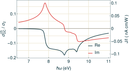
Figure 9 displays the resulting photoconductivity at low temperature for an undoped () hBN bilayer. Since is by far the largest energy scale in hBN, it is no surprise that the shape of seen here is almost entirely similar to that of the monolayer (cf. Fig. 3), except for a factor of 2 enhancement in the case of the bilayer on account of the system now having twice as many layers. The one noticeable difference appears associated with the van Hove singularities at the points of the BZ because, at these saddle points in the energy dispersion, the separation of the pair of valence (and conduction) bands is large (), leading to a sizable separation () of the two possible vertical transitions.
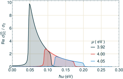
An interesting scenario is possible if the bilayer is slightly doped (possibly intentionally by impurities) in order to place the chemical potential at or slightly above the bottom of the lowest conduction band (the same happens if is slightly below the top of the highest valence band in a slightly hole-doped scenario)Terrones et al. (2007); Wei et al. (2011). Consider the results shown in Fig. 10(a). At the point the separation between bands 2 and 4 [cf. Fig. 7(d)] is
| (34) |
Since in hBN, this separation is rather small when compared with to leading order in the gap. As a result, transitions between bands open a channel for second order response at a very low energy () when compared with typical valence-conduction transitions. Consequently, when hBN is slightly electron-doped so that straddles the bottom of the two conduction bands one obtains: (i) a strong response at frequencies meV that can easily be an order of magnitude higher than the response characteristic of the valence-conduction transitions; (ii) an inversion of the sign of the induced current for low stimulating frequencies in comparison with that for frequencies above the fundamental band gap. The high intensity seen in the low frequency window shown in Fig. 10(a) stems from the fact that these processes arise from interband transitions between bands having approximately the same curvature [see Fig. 7(d)]. As a result, there is a much larger underlying joint density of states than at higher energies, where the transitions always connect states in bands with opposite curvature. The frequency band showing strong infrared response is controlled by the position of the chemical potential, suggesting that the effect can be manipulated by tailoring the doping level.
VI The role of excitons in hBN
Excitons are not a crucial element in elementary descriptions of the optical response of graphene. Even though they do lead to quantitative changes in the position of the van Hove singularities Yang et al. (2009) and, therefore, should be properly accounted for in quantitative comparisons with experimental data Kravets et al. (2010); Mak et al. (2014), their presence doesn’t introduce significant qualitative changes to the frequency dependence of the response functions Kravets et al. (2010). In particular, the low-frequency behavior is not visibly sensitive to the inclusion of excitonic corrections due mostly to the fact that graphene has no band-gap. In BBG, the band-gap allows for the absorption spectrum to be modified in the gap region due to excitons, but the screening from substrates is enough to make these corrections relatively small in comparison with a single particle description Park and Louie (2010).
Boron nitride is different. First principles calculations indicate that the linear optical conductivity of hBN is strongly renormalized by excitonic corrections Wirtz et al. (2006). This, although a fact common to all two-dimensional insulator crystals on account of the reduced screening of Coulomb interactions, leads to a particularly strong correction in hBN on because of its very large band-gap. The second-harmonic susceptibility of hBN studied in Ref. Pedersen, 2015 is entirely dominated by the two-particle spectrum and we expect the photoconductivity, , to be likewise strongly modified.
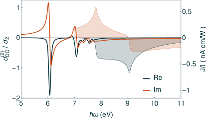
To that end, we have applied the two-band model Pedersen (2015) of the second-order intraband response to the non-linear photoconductivity in hBN. The band structure is based on the parameters applied above, i.e. and screening is implemented as in reference Pedersen, 2015. The resulting exciton spectrum is shown in Fig. 11, which should be contrasted with the independent-electron result in Fig. 3(a). For a direct comparison, the latter is reproduced as the shaded curves in Fig. 11. It is apparent that Coulomb effects cause a marked red-shift by nearly 2 eV of the onset of the photoconductive response: the prominent band-gap feature characteristic of the independent-electron response at 7.8 eV is down-shifted to the fundamental exciton energy around 6.1 eV. It is also noted that the magnitude of the response at frequencies associated with well isolated exciton levels is dramatically increased (in excess of tenfold) in comparison with the non-interacting case. At the same time, whereas the curve of is markedly structured in the frequency range containing well defined excitons, it becomes quite featureless above the non-interacting band-gap. This is a consequence of the large spectral weight carried by the excitonic peaks that implies a depletion in the response at frequencies above the band-gap. This is analogous to the behavior observed in the (linear) optical absorption spectrum of this material Wirtz et al. (2006). The colossal excitonic effects derive mainly from the poor screening in large-gap two-dimensional insulators, of which hBN is clearly an extreme case. In view of the close similarity between the photoconductivity of hBN monolayers and bilayers seen at the independent-particle level [cf. Figs. 3(a) and Fig. 9], we expect an equally strong renormalization of the response in the undoped bilayers. In general, less pronounced modifications are expected for low-gap systems such as bilayer graphene or other realizations of the more general “gapped graphene” model discussed above, as well as in the lightly doped scenarios discussed before.
VII Conclusion
The photoconductivity provides a direct measure of the ability to directly inject dc currents in a system by purely optical means. Harnessing and being able to tailor this effect can lead to improved optoelectronic device concepts and functionalities. Two-dimensional crystals are excellent materials to explore towards this end due to the intrinsic ease of integration in flat heterostructures, the possibility of controlling the electronic density through field effect, or the ability to modify their electronic structure by various types of surface modification. We have explored the photoconductivity of honeycomb-based electronic systems in monolayer and bilayer form and resorted to the examples of graphene and hBN for a definite illustration of its behavior in the cases of small and large band-gap.
Our calculations were done in the length-gauge within the framework originally discussed by Sipe and collaborators Aversa and Sipe (1995). In the systems derived from graphene, an independent-particle approach should provide a good qualitative and quantitative characterization of the response. We therefore trust that our results for BBG are entirely realistic, and similarly for those pertaining to the “gapped graphene” model, provided the gaps are kept small. In particular, our results in Sec. V.1 show that the ability to independently tune both the gap and density in BBG can lead to a very rich and density dependent photogalvanic response. On the other hand, those structures based on undoped hBN necessarily require an explicit treatment of the Coulomb interactions between particle-hole pairs. By solving the Bethe-Salpeter equation and computing the resulting photogalvanic response, we have shown in Sec. VI that the reduced screening in two-dimensions leads to robust excitons with large binding energies that, not only strongly renormalize the onset of the response to much lower energies, but, importantly, concentrate most of the spectral weight for . Therefore, similarly to their crucial impact in the absorption spectrum, interaction effects are clearly unavoidable in an accurate model of the photoconductivity for hBN. In a lightly doped scenario, however, the enhanced metallic screening is expected to significantly suppress the Coulomb interaction and bring the system’s response closer to that of an independent-particle description. Experiments reporting doping by carbon substitution have been reported in hBN films, nanotubes and nanoribbons Terrones et al. (2007); Wei et al. (2011). It has also been predicted that intercalation or adsorption with alkali elements can produce shallow donor states with minimal impact in the underlying band structure Oba et al. (2010). In this case, the features discussed in Sec. V.3 should hold, and one expects a strong photoconductivity in a narrow frequency band in the infra-red. The existence and width of this band are controlled by the position of the chemical potential within the two conduction sub-bands, and suggests the possibility of generating photogalvanic currents in hBN with frequencies much smaller than the fundamental band-gap.
Acknowledgements.
F.H. expresses thanks to A. H. Castro Neto for his support and discussions throughout this project. This work was supported by the National Research Foundation Singapore, under its Medium Sized Centre Programme and the CRP Award No. NRF-CRP6-2010-05. T.G.P. is financially supported by the CNG center under the Danish National Research Foundation, Project No. DNRF103, and the QUSCOPE center sponsored by the Villum foundation. The numerical computations were carried out at the HPC facilities of the Centre for Advanced 2D Materials at the National University of Singapore.References
- Bass et al. (1962) M. Bass, P. A. Franken, F. Ward, and G. Weinreich, Phys. Rev. Lett. 9, 446 (1962).
- Ivchenko (2005) E. L. Ivchenko, Optical Spectroscopy of Semiconductor Nanostructures (Alpha Science International, Ltd, 2005) p. 350.
- Ghosh and Mandel (1987) R. Ghosh and L. Mandel, Phys. Rev. Lett. 59, 1903 (1987).
- Shih and Alley (1988) Y. H. Shih and C. O. Alley, Phys. Rev. Lett. 61, 2921 (1988).
- Boyd (2008) R. W. Boyd, Nonlinear Optics, 3rd ed. (Elsevier Science Publishing Co Inc, 2008).
- Shen (2002) Y. R. Shen, The Principles of Nonlinear Optics (2002).
- Haussühl (2007) S. Haussühl, Physical Properties of Crystals, edited by S. Hausshl (Wiley-VCH Verlag GmbH, Weinheim, Germany, 2007).
- Zhang et al. (2009) Y. Zhang, V. W. Brar, C. Girit, A. Zettl, and M. F. Crommie, Nat. Phys. 5, 722 (2009).
- Castro et al. (2007) E. V. Castro, K. S. Novoselov, S. V. Morozov, N. M. R. Peres, J. M. B. L. dos Santos, J. Nilsson, F. Guinea, A. K. Geim, and A. H. C. Neto, Phys. Rev. Lett. 99, 216802 (2007).
- Das et al. (2008) A. Das, S. Pisana, B. Chakraborty, S. Piscanec, S. K. Saha, U. V. Waghmare, N. K. S., H. R. Krishnamurthy, A. K. Geim, A. C. Ferrari, and A. K. Sood, Nat. Nano. 3, 210 (2008).
- Aversa and Sipe (1995) C. Aversa and J. E. Sipe, Phys. Rev. B 52, 14636 (1995).
- Brun and Pedersen (2015) S. J. Brun and T. G. Pedersen, Phys. Rev. B 91, 205405 (2015).
- Trolle et al. (2014) M. L. Trolle, G. Seifert, and T. G. Pedersen, Phys. Rev. B 89, 235410 (2014).
- Pedersen (2015) T. G. Pedersen, Phys. Rev. B 92, 235432 (2015).
- Dresselhaus et al. (2008) M. S. Dresselhaus, G. Dresselhaus, and A. Jorio, Group Theory (Springer Berlin Heidelberg, Berlin, Heidelberg, 2008).
- Ribeiro and Peres (2011) R. M. Ribeiro and N. M. R. Peres, Phys. Rev. B 83, 235312 (2011).
- Sakurai (1967) J. J. Sakurai, Advanced Quantum Physics, 1st ed. (Addison-Wesley, Berlin, Heidelberg, 1967).
- Blount (1962) E. Blount, in Solid State Phys., Vol. 13 (1962) pp. 305–373.
- Moss et al. (1990) D. J. Moss, E. Ghahramani, J. E. Sipe, and H. M. van Driel, Phys. Rev. B 41, 1542 (1990).
- Berry (1984) M. V. Berry, Proc. R. Soc. A 392, 45 (1984).
- Xiao et al. (2010) D. Xiao, M.-C. Chang, and Q. Niu, Rev. Mod. Phys. 82, 1959 (2010).
- Gusynin and Sharapov (2006) V. P. Gusynin and S. G. Sharapov, Phys. Rev. B 73, 245411 (2006).
- Peres et al. (2006) N. M. R. Peres, F. Guinea, and A. Castro Neto, Phys. Rev. B 73, 125411 (2006).
- Stauber et al. (2008a) T. Stauber, N. M. R. Peres, and A. K. Geim, Phys. Rev. B 78, 085432 (2008a).
- Mak et al. (2008) K. F. Mak, M. Y. Sfeir, Y. Wu, C. H. Lui, J. A. Misewich, and T. F. Heinz, Phys. Rev. Lett. 101, 196405 (2008).
- (26) Given a linearly polarized electric field along , the photocurrent depends exclusively on the real part of the photoconductivity. Hence, the ratio between the electric curent per laser intensity to the real part of photoconductivity tensor in units of reads , where is refrective index, the vacuum permitivity and the speed of light in vacuum. For hBN or graphene based systems, the ratios are respectively.
- Sun et al. (2008) D. Sun, Z.-K. Wu, C. Divin, X. Li, C. Berger, W. A. de Heer, P. N. First, and T. B. Norris, Phys. Rev. Lett. 101, 157402 (2008).
- Ruzicka et al. (2010a) B. A. Ruzicka, S. Wang, L. K. Werake, B. Weintrub, K. P. Loh, and H. Zhao, Phys. Rev. B 82, 195414 (2010a).
- Ruzicka et al. (2010b) B. A. Ruzicka, L. K. Werake, H. Zhao, S. Wang, and K. P. Loh, App. Phys. Lett. 96, 173106 (2010b).
- Lui et al. (2010) C. H. Lui, K. F. Mak, J. Shan, and T. F. Heinz, Phys. Rev. Lett. 105, 127404 (2010).
- Sun et al. (2012) D. Sun, G. Aivazian, A. M. Jones, J. S. Ross, W. Yao, D. Cobden, and X. Xu, Nat. Nanotechnol. 7, 114 (2012).
- Tielrooij et al. (2013) K. J. Tielrooij, J. C. W. Song, S. A. Jensen, A. Centeno, A. Pesquera, A. Zurutuza Elorza, M. Bonn, L. S. Levitov, and F. H. L. Koppens, Nat. Phys. 9, 248 (2013).
- Jorio et al. (2011) A. Jorio, R. Saito, G. Dresselhaus, and M. S. Dresselhaus, Raman Spectroscopy in Graphene Related Systems (Wiley-VCH Verlag GmbH & Co. KGaA, Weinheim, Germany, 2011).
- Giovannetti et al. (2007) G. Giovannetti, P. A. Khomyakov, G. Brocks, P. J. Kelly, and J. van den Brink, Phys. Rev. B 76, 073103 (2007).
- Zhou et al. (2007) S. Y. Zhou, G.-H. Gweon, a. V. Fedorov, P. N. First, W. A. de Heer, D.-H. Lee, F. Guinea, A. H. Castro Neto, and A. Lanzara, Nat. Mater. 6, 916 (2007).
- Sławińska et al. (2010) J. Sławińska, I. Zasada, and Z. Klusek, Phys. Rev. B 81, 155433 (2010).
- Dean et al. (2010) C. R. Dean, A. F. Young, I. Meric, C. Lee, L. Wang, S. Sorgenfrei, K. Watanabe, T. Taniguchi, P. Kim, K. L. Shepard, and J. Hone, Nat. Nanotechnol. 5, 722 (2010).
- Ortix et al. (2012) C. Ortix, L. Yang, and J. van den Brink, Phys. Rev. B 86, 081405 (2012).
- Chen et al. (2014) Z.-G. Chen, Z. Shi, W. Yang, X. Lu, Y. Lai, H. Yan, F. Wang, G. Zhang, and Z. Li, Nat. Commun. 5, 4461 (2014).
- Bokdam et al. (2014) M. Bokdam, T. Amlaki, G. Brocks, and P. J. Kelly, Phys. Rev. B 89, 201404 (2014).
- Woods et al. (2014) C. R. Woods, L. Britnell, A. Eckmann, R. S. Ma, J. C. Lu, H. M. Guo, X. Lin, G. L. Yu, Y. Cao, R. V. Gorbachev, A. V. Kretinin, J. Park, L. A. Ponomarenko, M. I. Katsnelson, Y. N. Gornostyrev, K. Watanabe, T. Taniguchi, C. Casiraghi, H.-j. Gao, A. K. Geim, and K. S. Novoselov, Nat. Phys. 10, 451 (2014).
- Yankowitz et al. (2014) M. Yankowitz, J. Xue, and B. J. LeRoy, J. Phys. Condens. Matter 26, 303201 (2014).
- Huang et al. (2014) L. Huang, Q. Yue, J. Kang, Y. Li, and L. Jingbo, J. Phys. Condens. Matter 26, 295304 (2014).
- Pedersen and Pedersen (2009) T. G. Pedersen and K. Pedersen, Phys. Rev. B 79, 035422 (2009).
- McCann and Fal’ko (2006) E. McCann and V. I. Fal’ko, Phys. Rev. Lett. 96, 086805 (2006).
- Szafranek et al. (2011) B. N. Szafranek, D. Schall, M. Otto, D. Neumaier, and H. Kurz, Nano Lett. 11, 2640 (2011).
- Velasco et al. (2012) J. Velasco, L. Jing, W. Bao, Y. Lee, P. Kratz, V. Aji, M. Bockrath, C. N. Lau, C. Varma, R. Stillwell, D. Smirnov, F. Zhang, J. Jung, and A. H. MacDonald, Nat. Nanotechnol. 7, 156 (2012).
- Pachoud et al. (2010) A. Pachoud, M. Jaiswal, P. K. Ang, K. P. Loh, and B. Oezyilmaz, EPL 92, 27001 (2010).
- Britnell et al. (2012) L. Britnell, R. V. Gorbachev, R. Jalil, B. D. Belle, F. Schedin, A. Mishchenko, T. Georgiou, M. I. Katsnelson, L. Eaves, S. V. Morozov, N. M. R. Peres, J. Leist, A. K. Geim, K. S. Novoselov, and L. A. Ponomarenko, Sci. 335, 947 (2012).
- Stabile et al. (2015) A. A. Stabile, A. Ferreira, J. Li, N. M. R. Peres, and J. Zhu, Phys. Rev. B 92, 121411 (2015).
- Peres et al. (2008) N. M. R. Peres, T. Stauber, and A. Castro Neto, EPL 84, 38002 (2008).
- Stauber et al. (2008b) T. Stauber, N. M. R. Peres, and A. H. Castro Neto, Phys. Rev. B 78, 085418 (2008b).
- Stauber and Peres (2008) T. Stauber and N. M. R. Peres, J. Phys. Condens. Matter 20, 055002 (2008).
- Abergel et al. (2012) D. S. L. Abergel, H. Min, E. H. Hwang, and S. Das Sarma, Phys. Rev. B 85, 045411 (2012).
- Yuan et al. (2011) S. Yuan, R. Roldán, H. De Raedt, and M. I. Katsnelson, Phys. Rev. B 84, 195418 (2011).
- Gannett et al. (2011) W. Gannett, W. Regan, K. Watanabe, T. Taniguchi, M. F. Crommie, and A. Zettl, Appl. Phys. Lett. 98, 242105 (2011).
- Chari et al. (2015) T. Chari, I. Meric, C. Dean, and K. Shepard, IEEE Trans. Electron Devices 62, 4322 (2015).
- Banszerus et al. (2016) L. Banszerus, M. Schmitz, S. Engels, M. Goldsche, K. Watanabe, T. Taniguchi, B. Beschoten, and C. Stampfer, Nano Lett. 16, 1387 (2016).
- Ni et al. (2016) G. X. Ni, L. Wang, M. D. Goldflam, M. Wagner, Z. Fei, A. S. McLeod, M. K. Liu, F. Keilmann, B. Özyilmaz, A. H. Castro Neto, J. Hone, M. M. Fogler, and D. N. Basov, Nat. Photon. 10, 244 (2016).
- Pallecchi et al. (2014) E. Pallecchi, F. Lafont, V. Cavaliere, F. Schopfer, D. Mailly, W. Poirier, and A. Ouerghi, Sci. Rep. 4, 4558 (2014).
- Yang and Ni (2010) Z. Yang and J. Ni, J. Appl. Phys. 107, 104301 (2010).
- Terrones et al. (2007) M. Terrones, J. M. Romo-Herrera, E. Cruz-Silva, F. López-Urías, E. Muñoz-Sandoval, J. J. Velázquez-Salazar, H. Terrones, Y. Bando, and D. Golberg, Mater. Today 10, 30 (2007).
- Wei et al. (2011) X. Wei, M.-S. Wang, Y. Bando, and D. Golberg, ACS Nano 5, 2916 (2011).
- Yang et al. (2009) L. Yang, J. Deslippe, C. H. Park, M. L. Cohen, and S. G. Louie, Phys. Rev. Lett. 103, 186802 (2009).
- Kravets et al. (2010) V. G. Kravets, A. N. Grigorenko, R. R. Nair, P. Blake, S. Anissimova, K. S. Novoselov, and A. K. Geim, Phys. Rev. B 81, 155413 (2010).
- Mak et al. (2014) K. F. Mak, F. H. da Jornada, K. He, J. Deslippe, N. Petrone, J. Hone, J. Shan, S. G. Louie, and T. F. Heinz, Phys. Rev. Lett. 112, 207401 (2014).
- Park and Louie (2010) C. H. Park and S. G. Louie, Nano Lett. 10, 426 (2010).
- Wirtz et al. (2006) L. Wirtz, A. Marini, and A. Rubio, Phys. Rev. Lett. 96, 126104 (2006).
- Oba et al. (2010) F. Oba, A. Togo, I. Tanaka, K. Watanabe, and T. Taniguchi, Phys. Rev. B 81, 075125 (2010).