Well-Posed Models of Memristive Devices
Abstract
Existing compact models for memristive devices (including RRAM and CBRAM) all suffer from issues related to mathematical ill-posedness and/or improper implementation. This limits their value for simulation and design and in some cases, results in qualitatively unphysical predictions. We identify the causes of ill-posedness in these models. We then show how memristive devices in general can be modelled using only continuous/smooth primitives in such a way that they always respect physical bounds for filament length and also feature well-defined and correct DC behaviour. We show how to express these models properly in languages like Verilog-A and ModSpec (MATLAB). We apply these methods to correct previously published RRAM and memristor models and make them well posed. The result is a collection of memristor models that may be dubbed “simulation-ready”, i.e., that feature the right physical characteristics and are suitable for robust and consistent simulation in DC, AC, transient, etc., analyses. We provide implementations of these models in both ModSpec/MATLAB and Verilog-A.
I Introduction
In 1971, Leon Chua noted [1] that while two-terminal circuit elements relating voltage and current (i.e., resistors), voltage and charge (capacitors) and current and flux (inductors) were well known, no element that directly relates charge and flux seemed to exist. He explored the properties of this hypothetical element and found that its voltage-current characteristics would be those of a resistor, but that if the element were nonlinear, its resistance would change with time and be determined by the history of biasses applied to the device. In other words, the instantaneous resistance of the element would retain some memory of past inputs. Chua dubbed this missing element a “memristor”, and showed that a telltale characteristic was that its – curves would always pass through , regardless of how it was biassed as a function of time.111i.e., a memristor’s – characteristics are “pinched” at the origin. Long after Chua’s landmark observation, devices with memristive behaviour were found in nature, e.g., in the well-publicized nano-crossbar device of Stan Williams and colleagues [2, 3], and others as well [4, 5]. It was also realized that many physically observed devices prior to [2, 3] were in fact memristors [6, 7, 8].
Physically, present-day memristive nano-devices typically operate by forming and destroying conducting filaments through an insulating material sandwiched between two contacts separated by a small distance . The conducting filaments can be of different types. For example, they can consist of oxide vacancies, by filling which electrons can flow, as in RRAM (Resistive Random Access Memory [9]). In CBRAM (Conductive Bridging RAM [10]), metal ions222various metals, including Cu, Ag, W, Sn and Cr, have been used. that infiltrate the insulator form the conducting filament. In memristors made of Si-impregnated silica [11], conduction occurs via tunnelling between traps. Depending on the magnitude and polarity of the voltage applied, the conducting filaments can lengthen or shorten; it is their length that determines the resistance of the device. Basic geometry indicates that the length of the filament(s) must always be between zero (i.e., there is no filament) and the distance between the contacts (i.e., the filament connects the two contacts) — in other words, the length of the filament(s) must never be outside the range . Another basic property is that when the voltage across the device has one polarity (say positive), the filament grows until it reaches its maximum length , at which it settles; whereas for the opposite polarity (say negative), the filament shrinks until it reaches its minimum length . Therefore, if a positive DC voltage is applied, the DC (i.e., long term) response of the memristor’s filament length must be ; whereas if a negative DC voltage is applied, its DC response must be .
A number of novel circuits based on memristors have been proposed [12, 13], most of which use crossbar architectures for non-volatile memory [14, 15] and neuromorphic computing [16, 17, 18] applications. To support their design, various compact models of memristors, purportedly suitable for simulation in SPICE-like simulators, have been published. However, our attempts to use these models have revealed shortcomings serious enough to preclude their general use for simulation or design. Broadly speaking, these existing models suffer from ill-posedness issues; e.g., they are not properly defined at all biasses, or their outputs are not unique, or they suffer from continuity/smoothness problems. Well-posedness [19, 20]333A well-posed mathematical model of a physical device should have the properties that a unique solution or output should exist for any given input, and that outputs should vary smoothly with respect to inputs and parameters. is a fundamental requirement for models meant to represent physical reality and is also crucial for numerical algorithms using the models to work properly.
The well-posedness requirement applies not only to memristive devices, but to any model meant for simulation. To appreciate why, it is important to realize that a model represents a mathematical abstraction of a physical device. While this abstraction must represent reality well enough to be useful for prediction, it must also be suitable for use with numerical simulation algorithms. To be so, it needs to satisfy certain important mathematical properties, the most basic and universal of which is well posedness.
To illustrate how a well-posed mathematical model must often be “more than” the physical device it represents, consider the question: is it necessary to model a device outside regions that are physically reasonable in proper operation?444This is a frequent point of confusion amongst compact model developers. For example, should a compact model of a memristor (or a diode, or resistor, or IC MOSFET), be “valid” at a bias of a million volts (at which, in reality, most physical devices would simply burn up)? The answer to this question is yes – indeed, it has been a standard requirement for device models (including resistors, capacitors, diodes, BJT and MOS devices, etc.) in SPICE-like simulators to evaluate successfully and provide unique, smoothly varying outputs at all biasses, including large, physically unrealistic, biasses. These requirements stem not only from the numerical algorithms used by simulators (in particular, the Newton-Raphson (NR) algorithm for solving nonlinear equations [21]), but also from the iterative methodology using which circuits are typically designed:
-
1.
In the process of converging to a valid solution of the circuit, NR typically applies a sequence of biasses to devices; many of these biasses can be large or physically unreasonable. Compact models must be designed to evaluate successfully and be smooth at every bias applied, whether it is physically reasonable or not, in order for NR to go about trying to find a solution [22, 23]. If devices are modelled well and the circuit has been designed properly, then, at the solution found by NR, biasses to devices can be expected to be physically reasonable.
-
2.
Even if NR converges to a solution that is physically unreasonable, the “bad” solution has value in circuit design, for it typically provides quantitative insight into what is wrong with the design. A compact model that refuses to evaluate or generates a floating-point error prevents such solutions, and the insights they provide, from being found.
Common ill-posedness mechanisms in models include division-by-zero errors, often due to expressions like , which become unbounded (and feature a “doubly infinite” jump) at ; the use of or without ensuring that their arguments are always positive, regardless of bias; the fundamental misconception that non-real (i.e., complex) numbers or infinity are legal values for device models (they are not!); and “sharp”/“pointy” functions like , whose derivatives are not continuous.
Another key aspect of well-posedness is that the model’s equations must produce mathematically valid outputs for any mathematically valid input to the device. Possibly the most basic kind of input is one that is constant (“DC”) for all time. DC solutions (“operating points”) are fundamental in circuit design; they are typically the kind of solution a designer seeks first of all, and are used as starting points for other analyses like transient, small signal AC, etc. If a model’s equations do not produce valid DC outputs given DC inputs, it fails a very fundamental well-posedness requirement. For example, the equation is ill posed, since no DC (constant) solution for the output is possible if the input is any non-zero constant. Such ill posedness is typically indicative of some fundamental physical principle being violated; for example, in the case of , the system is not strictly stable [24]. Indeed, a well-posed model that is properly written and implemented should work consistently in every analysis (including DC, transient, AC, etc.).555Different analyses correspond to different ways of exciting the device, or to finding specific kinds of outputs. For example, periodic steady state analyses excite the device with time-periodic inputs, and seek similarly time-periodic outputs.
In spite of seemingly significant efforts to devise memristor models, every model we are aware of666We request the reader to contact us if he/she is aware of published, openly available and reproducible memristor models prior to this work (other than the ones noted here), especially if they do not suffer from ill-posedness issues. in the literature [25, 26, 27, 28, 29, 30] suffers from one or more of the above-mentioned types of ill-posedness. The University of Michigan model [25], many aspects of which have been adopted by later models, suffers from division-by-zero errors and DC response problems. An RRAM model from Stanford/ASU with several variants [26, 27, 28, 29, 31, 32, 33, 34] that has received considerable publicity suffers from egregious DC response problems.777To their credit, the authors of [27] explicitly note this deficiency in their model’s documentation. The UESTC memristor models [30], though they avoid many issues common to other models, still suffer from subtle (but serious) DC response problems. The TEAM models for general memristors [31, 32, 33, 34] also suffer from DC, uniqueness and continuity/smoothness issues. Over and above well-posedness issues, released versions of existing memristor compact models frequently suffer from deficiencies in the way their equations are expressed in modelling languages like Verilog-A. Examples of deficiencies we have encountered include attempts to perform time-integration of differential equations within the model definition, inserting time-varying noise terms as an integral part of the model, using integral formulations instead of differential ones, etc. As explained in [23], such practices compromise accuracy, limit the model’s ability to support all analyses, reduce portability across simulators, and so on. Further details about the shortcomings we have observed in these models are provided later in this paper.
In this paper, we explain the correct generic way to model memristive devices in a well-posed manner. Our modelling technique sets up the dynamics of the filament length using a differential equation, and the current-voltage relationship of the memristor using an algebraic equation involving the filament length. Employing only continuous/smooth mathematical constructs, we show how filament dynamics can be modelled such that physical bounds are always respected and correct DC behaviour for positive and negative biasses always results. In the process of developing our modelling technique, we pinpoint several common mechanisms underlying ill-posedness in prior models. Since filament dynamics in memristive devices have features closely related to hysteresis,888Memristive devices may be said to be at the “cusp of hysteresis”. we explain how to model hysteresis correctly in general, then apply this to memristive devices. We use our techniques to correct several previous models, making them well posed and suitable for any analysis (including DC, transient, AC, periodic steady state, etc.). The process of restoring well-posedness to memristor models also provides insights into possible physical mechanisms in memristors that seem not to have been looked into yet.
The remainder of the paper is organized as follows. In Sec. II, we explain how hysteresis should be modelled in general, i.e., using internal unknown variables and implicit equations. We illustrate how a model with internal unknowns and implicit equations can be written properly in both Verilog-A [35, 36, 23, 37] and ModSpec [38, 39]. In Sec. IV, we specialize our general model template for hysteresis to RRAM devices, showing how to design the continuous/smooth equations involved so that filament length boundaries are always respected and the correct DC behaviour results. We write well-posed RRAM models in both Verilog-A and ModSpec and test them in simulation, using DC, transient and homotopy [40] analyses.999Homotopy analysis provides considerable insight into RRAM behaviour. Then, in Sec. V, we develop techniques for aiding numerical convergence in the RRAM model. In particular, we design a SPICE-compatible limiting function for the rapidly-growing hyperbolic sine function used in the RRAM model, inspired by the limiting functions used in SPICE’s non-linear semiconductor devices. To our knowledge, this is the first limiting function designed to aid convergence after PNJLIM and FETLIM, which were developed as part of the original Berkeley SPICE [41]. Next, in Sec. VI, we study all the published compact models for memristors we are aware of that come with concrete equations or code. We identify issues of ill-posedness and poor implementation that affect their applicability in simulation. We then use our modelling techniques to correct their problems and turn them into well-posed models, providing proper implementations in ModSpec and Verilog-A.
The result of our study is a collection of well-posed, properly implemented, compact models for memristive devices. Specifically, we devise 5 different algebraic current-voltage and 6 different differential equation dynamical models for filament length, i.e., 30 different models for memristors and/or RRAM devices, all well posed.
Although we use underlying equations published by others, we modify them to remove ill-posedness issues, and also provide proper implementations. Understanding the process by which we do this can be valuable for the development of future models, not only of memristors, but of other hysteretic devices as well.
II How to Model Hysteresis Properly
To develop our memristor models, we first study how to model – hysteresis in two-terminal devices properly. We show that the – hysteresis can be modelled with the help of an internal state variable and an implicit differential equation. Then with the help of an example, we illustrate how a model with internal unknowns and implicit equations can be properly written in both Verilog-A and the ModSpec format.
II-A Model Template for Devices with – Hysteresis
The equation of a general two-terminal resistive device can be written as
| (1) |
where is the voltage across the device, the current through it. For example, the function for a simple linear resistor can be written as
| (2) |
For devices with – hysteresis, and cannot have a simple algebraic mapping like (1). Instead, we introduce a state variable into (1) and rewrite the – relationship as
| (3) |
The dynamics of the internal state variable is governed by a differential equation:
| (4) |
The internal state variable can have several physical meanings. If we consider the original memristor model proposed by Chua in the 1970s [1, 42], can be thought of as the flux or charge stored in the device. In the context of metal-insulator-metal-(MIM)-structured RAM devices, e.g., RRAMs and CBRAMs, can represent either the length of the conductive filament/bridge, or the gap between the tip of the filament/bridge to the opposing electrode.101010For CBRAM devices, the tunnelling gap can also form in the middle of the conductive bridge instead of on one of its ends [43].
In all these scenarios, has some influence on . So we cannot directly calculate the current based on the voltage applied to the device at a single time ; also depends on the value of . On the other hand, at time , the value of is determined by the history of according to (4). Therefore, we can think of the device as having internal “memory” of the history of its input voltage. If we choose the formula for and in (3) and (4) properly, as we sweep the voltage, hysteresis in the current becomes possible.
In the rest of this paper, (3) and (4) serve as a model template for two-terminal devices with – hysteresis. To illustrate its use, we design a device example, namely “hys_example”, with functions and defined as follows.
| (5) |
| (6) |
The choice of is easy to understand. is a monotonically increasing function with range . We add to it to make its range positive. We then incorporate it into as a factor such that can modulate the conductance of the device between and .
The choice of determines the dynamics of . And when , the corresponding (, ) pairs will show up as part of the DC solutions of circuits containing this device. Therefore, if we plot the values of in a contour plot, such as in Fig. 1 (a), the curve representing is especially important. Through the use of a simple cubic polynomial of in (6), we design the curve to fold back in the middle, crossing the axis three times. In this way, when is around , there are three possible values can settle on, all satisfying . This multiple stability in state variable is the foundation of hysteresis found in the DC sweep on the device.
Fig. 1 (b) illustrates how hysteresis takes place in DC sweeps. In Fig. 1 (b), we divide the curve into three parts: curve A and B have positive slopes while C has a negative one. When we sweep towards the right at a very slow speed to approximate DC conditions, starting from a negative value left of , at the beginning, there is only one possible DC solution of . As we increase , the (, ) pair will move along curve A, until A ends when reaches . If increases slightly beyond , multiple stability in disappears. (, ) reaches the region and will grow until it reaches the B part of the curve. This shows up in the DC solutions as a sudden jump of towards curve B. Similarly, when we sweep in the other direction starting from the right of , the (, ) pair will follow curve B, then have a sudden shift to A at . Because , hysteresis occurs in when sweeping , as illustrated in Fig. 1 (b). Since modulates the device’s conductance, there will also be hysteresis in the – relationship.
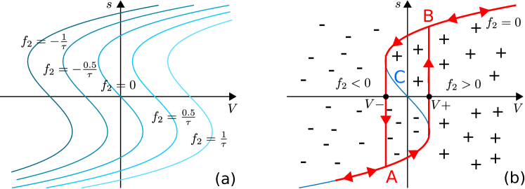
Note that we are analyzing and predicting hysteresis based on the DC solution curve defined by . This clarifies a common confusion people have. As hysteresis is normally defined as a type of time-dependence between output and input, people often believe that it has nothing to do with the circuit’s or device’s DC properties. It is true that hysteresis is normally observed in transient analysis. But from the above discussions, we can see that it is indeed generated by the multiple stability and the abrupt change in DC solutions. As mentioned earlier, at a certain time , can be thought of as encoding the memory of from the past. Its multiple stability reflects the different possible sets of history of . And the separation between and in the DC curves ensures that no matter at what speed we sweep , there will always be hysteresis in the – relationship.
When we sweep back and forth, curve C, the one with a negative slope in Fig. 1 (b) never shows up in solutions. The reason is that, although it also consists of solutions of , these solutions are not stable. If a (, ) point on curve C is perturbed to move above C, whether because of physical noise or numerical error, it falls in the region and will continue to grow until it reaches B. Similarly, if it moves below C, it will decrease to curve A. Therefore, it won’t be observed during voltage sweep, leaving only A and B to form the – hysteresis curves.
II-B Compact Model in MAPP
With the model equations for hys_example defined in (5) and (6), how do we put them into a compact model so that we can simulate it in circuits? To answer this question, in this section, we first discuss our formulation of the general form of device compact models, namely the ModSpec format [38, 39]. Then we develop the ModSpec model for hys_example and implement it in MAPP [44].
ModSpec is MAPP’s way of specifying device models. A device model describes the relationship between variables using equations. Among the variables of interest, some are the device’s inputs/outputs; they are related to the circuit connectivity. We call them the device’s I/Os. In the context of electrical devices, they are branch voltages and currents. Among all the I/Os, some may be expressed explicitly using the other variables; they are the outputs of the model’s explicit equations. Furthermore, a device model can also have non-I/O internal unknowns and implicit equations. Taking all these possibilities into consideration, we specify model equations in the following ModSpec format.
| (7) | |||||
| (8) |
Vectors and contain the device’s I/Os: comprises those I/Os that can be expressed explicitly (for hys_example, it contains only ), while comprises those that cannot (for hys_example, it is ). contains the model’s internal unknowns (for hys_example, it is ), while provides a mechanism for specifying time-varying inputs within the device (e.g., as in independent voltage or current sources). The functions , , and define the differential and algebraic parts of the model’s explicit and implicit equations.
For hys_example, we can write its model equations in the ModSpec format as follows.
| (9) |
with , , , .
We can enter the model information in (9) into MAPP by constructing a ModSpec object MOD. The code in Appendix A-A shows how to create this device model for hys_example entirely in the MATLAB language. For more detailed description of the ModSpec format, users can issue the command “help ModSpec_concepts” in MAPP.
II-C Simulation Results
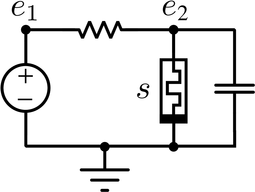
In this section, we verify our analysis and prediction of – hysteresis in Sec. II-A by testing the compact models presented in Sec. II-B and in a circuit shown in Fig. 2.

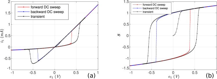
Fig. 3 shows the results from DC sweep and transient simulation with input voltage sweeping up and down on the circuit in Fig. 2. It confirms that hysteresis takes place in both – and – relationships of the device.
In Fig. 3 (b), curve C (defined in Fig. 1 (b)) with a negative slope never shows up in either forward or backward voltage DC sweep. This matches our discussion in Sec. II-A. In order to plot this curve and complete the DC solutions, also to get rid of the abrupt change of solutions in DC sweeps, we can use the homotopy analysis [40]. Homotopy analysis can track the DC solution curve in the state space.
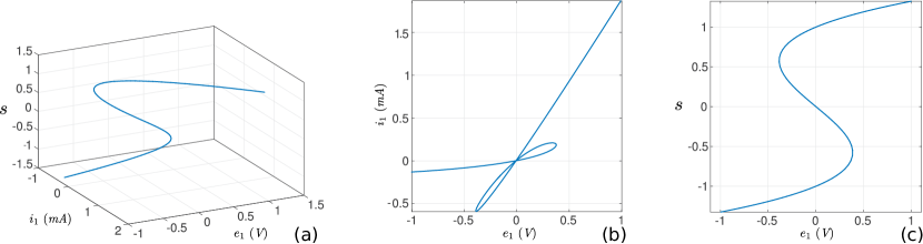
Results from homotopy analysis on the circuit in Fig. 2 are shown in Fig. 4. We note that all the circuit’s DC solutions indeed form a smooth curve in the state space. The side view of the 3-D plot displays curve C we have designed in our model equation (6). The corresponding curve in the top view connects the two discontinuous DC sweep curves in Fig. 3; it consists of all the unstable solutions in the – relationship. This curve was previously missing in DC and transient sweep results, and now displayed by the homotopy analysis. These results from homotopy analysis provide us with important insights into the model. They reveal that there is a single smooth and continuous DC solution curve in the state space, which is an indicator of the well-posedness of the model. They also illustrate that it is the folding in the smooth DC solution curve that has created the discontinuities in DC sweep results. These insights are important for the proper modelling of hysteresis.
Moreover, the top view explains the use of internal state for modelling hysteresis from another angle. Without the internal state, it would be difficult if not impossible to write a single equation describing the – relationship shown in Fig. 4 (b). With the help of , we can easily choose two simple model equations as (5) and (6), and the complex – relationship forms naturally.
III How to Model Internal Unknowns Properly in Verilog-A
In this section, we write the hys_example model in the Verilog-A language.
Apart from the differences in syntax, Verilog-A differs from ModSpec in one key aspect — the way of handling internal unknowns and implicit equations. Verilog-A models a device with an internal circuit topology, i.e., with internal nodes and branches defined just like in a subcircuit. The variables in a Verilog-A model, the “sources” and “probes”, are potentials and flows specified based on this topology. Coming from this subcircuit perspective, the language doesn’t provide a straightforward way of dealing with general internal unknowns and implicit equations inside the model, e.g., the state variable and the equation (4) in hys_example.
This limitation gives rise to so much confusion about the modelling of devices with hysteresis, that we would like to examine the common modelling mistakes and pitfalls before describing our approach. Here is the list of how not to model internal unknowns and implicit equations in Verilog-A.
-
Declare the internal unknown as a general variable, e.g., using “real”, then use “idt()” function to describe the differential equation the variable should satisfy. This approach is not recommended because of several reasons.
First, Verilog-A provides most consistent definitions and support for potentials and flows as circuit unknowns; it is unclear how “real” variables inside differential equations are handled by each Verilog-A compiler. Some simulators will return inconsistent or incorrect results. Moreover, another potential hazard from this practice is that the simulator may create a memory state for the variable [23], limiting its use in some simulation algorithms, e.g., those for periodic steady state (PSS) analysis.
Also, people often attempt to use “idt()” in this scenario, apparently because Verilog-A doesn’t allow using “ddt()” to contribute to a none-potential/flow quantity as “source”, for good reasons. But this “workaround” with the use of “idt()” is not recommended [23, 36], as different simulators have inconsistent support for “idt()”.
-
Another pitfall is to use implicit contributions. While an implicit contribution in Verilog-A seems to simplify the code, and forces users to model the internal unknown as a potential or flow, which is in line with what we propose, it is not recommended [23, 37]. In fact, it is not supported properly even by some well-known commercial simulators.
-
Model the differential relationship by coding time integration inside. In this approach, the model has access to the absolute time and calculates the time step inside, then approximates the differential equation (4) by integrating at each time step. The approach may seem straightforward, but it has so many problems that I have to create another list for them:
-
The method can only use Forward Euler (FE) [22] internally for integration, potentially causing convergence issues for stiff systems.
-
In this method, the internal unknown is intentionally defined as a memory state, again creating difficulties for PSS simulation.
-
The model won’t perform correctly in analyses that do not involve time integration, like DC, small signal AC analysis and Harmonic Balance.
-
Even for transient simulation, it defeats the purpose of using the simulator, as it bypasses the simulator’s many built-in facilities, e.g., convergence aiding techniques, truncation error estimation, time step control, etc.
-
There are many more issues with this approach. For example, circuit designers cannot set transient analysis initial conditions for the internal unknown the normal way they do for capacitor voltages and inductor currents. Also, to “ensure” the accuracy of internal time integration, “bound_step” is often used. And the bounded step specified either makes simulation inaccurate or unnecessarily slow.
We note that these problems and pitfalls arise partly from the limitation of the Verilog-A language in intuitively handling general internal unknowns and implicit equations, mostly from bad modelling practices. To circumvent these issues and write a robust Verilog-A model for hys_example that should work consistently in all simulators and all simulation algorithms, we model state variable as a voltage. We declare an internal branch, whose voltage represents . One end of the branch is an internal node that doesn’t connect to any other branches. In this way, by contributing and ddt(-tau * s) both to this same branch, the KCL at the internal node will enforce the implicit differential equation in (6).
Declaring as a voltage is not the only way to model hys_example in Verilog-A. Depending on the physical nature of , one can also use Verilog-A’s multiphysics support and model it as a mechanical property, such as a position from the kinematic discipline. This may be closer to the actual meaning of for MIM-structured RAM devices. Alternatively, we can also use the property for potential from the thermal or magnetic discipline. One can also switch potential and flow by defining as a flow instead. These alternatives may make the model look more physical, but they do not make a difference mathematically, except from the scale of tolerances in each discipline, which we will discuss in more detail in Sec. IV-C. The essence of our approach is to recognize that state variable is a circuit unknown, and thus should be modelled as a potential or flow in Verilog-A, for the consistent support from different simulators in various circuit analyses.
The Verilog-A code for hys_example is provided in Appendix A-B. It generates consistent results in many simulation platforms, including Spectre,111111Spectre version: 7.2.0 64bit. HSPICE,121212HSPICE version: J-2014.09 64bit. and the open-source simulator Xyce.131313Xyce version: 6.4. The test benches with all these simulators can be found in Appendix A.
IV RRAM Model
The model hys_example developed in Sec. II is a model template for devices with hysteresis, such as RRAM devices. By changing its (5) and (6) functions in model equations, as well as the corresponding function implementations in MAPP and Verilog-A code, we can then have compact models capturing the physics of RRAM devices.
IV-A Model Equations
An RRAM device consists of two metal electrodes, namely (top) and (bottom), and a thin oxide film separating them. A conductive filament can form in the film. When it grows to connect the two electrodes, the device is in low resistance state (LRS); when part of it dissolves, the device enters high resistance state (HRS). As a RAM, its “memory” is stored in the status of its internal conductive filament and the corresponding resistance state.
From the above discussion, the internal state variable for RRAM models can be either the length of the filament [25], or the gap between the tip of the filament and the opposing electrode [26, 27]. We choose to use the gap in this section, as it is what really determines the tunnelling current. Then the variables in the RRAM model are: the voltage across the device, the current through it and the internal unknown . We can then rewrite the equations (3) and (4) from the model template in Sec. II-A as
| (10) | |||||
| (11) |
The physical contexts of these RRAM model equations are straightforward to understand. Equation (10) determines how the current is modulated by both the voltage and ; equation (11) describes the growth rate of at a given voltage with some existing size. Our goal of RRAM modelling is to find suitable and functions to capture these physical properties.
The formula for are mostly consistent across several existing RRAM models developed in different groups [25, 27, 29, 32]. Among them, [27, 29] use the same equation, which is only different from that used in [32] in the choice of internal unknown.141414In the I-V relationship equation in [32], we can redefine the internal unknown and make a one-to-one mapping between and , to make the equation equivalent to the one in [27, 29]. Therefore, in this section, we choose to use the function in [27, 29]:
| (12) |
where , , are fitting parameters.
For , we can adapt the growth formulation in [27, 29] and write it as
| (13) |
where , , are fitting parameters, is the thickness of the oxide film, is the thermal voltage, and
| (14) |
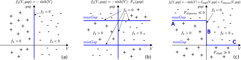
in (14) is known as the local field enhancement factor [45]. It accounts for the abrupt SET (filament grows enough to connect electrodes) and gradual RESET (filament dissolves) behaviors in bipolar RRAM devices [46]. Parameters are normally chosen to ensure that this factor is always positive. So the sign and zero-crossings of in (13) are determined only by .
While there are small differences among the functions in models developed by various groups [25, 27, 29, 32], they differ mainly in the definitions of fitting parameters. A property they all share is that the sign of is the same as that of . Put in other words, begins to decrease whenever is positive, and vice versa, as illustrated in Fig. 5 (a). While there is some physical truth to this statement, considering that an RRAM device will eventually be destroyed151515Under constant negative voltages, the filament will dissolve to the extent that SET cannot restore it. The device will need to go through the forming process again. Under constant positive voltages, the filament will grow too thick to RESET, and the device becomes shorted. if applied a constant voltage for an indefinite amount of time, for the model to work in numerical simulation, the state variable has to be bounded.
Ensuring that the upper and lower bounds for are always respected in simulation is one major challenge for the compact modelling of RRAM devices. To address this challenge, several techniques have been attempted in the existing RRAM compact models:
-
Directly use if-then-else statements on [27, 29]. This type of model is normally written in Verilog-A. They declare gap as a real variable, then directly enforce “if (gap < 0) gap = 0;”. We have discussed in great detail in Sec. III about the problems of modelling internal unknowns as general Verilog-A variables. On top of these problems, no matter whether the Verilog-A compiler treats gap as a circuit unknown or a memory state, the use of if-then-else statements for bounding the variable excludes the model from the differential equation framework. Thus they are not suitable for simulation analyses.
Moreover, the use of if-then-else also introduces hard discontinuities in the model, causing convergence problems [22]. Also, forcefully setting variable gap to certain values can result in singular circuit Jacobian matrices, creating difficulties for most simulation algorithms.
-
The goal is to set when and . The method used in these models is to multiply the in (13) with a window function that is close to when , equal to when is at or , and has negative values elsewhere. Directly constructing such windows functions with step() functions [25] is not recommended as it introduces discontinuities into the model. One better example of such window functions for window size is known as the Joglekar window [33]:
(15) where is a positive integer used to adjust the sharpness of the window.
After multiplying window functions, the function used in these models is still smooth and continuous, and the models still in the differential equation format, complying with the model template we have discussed in Sec. II. As a result, the models are often reported to run reasonably well in transient simulations [34, 33, 31].
However, there are subtle and deeper problems with this approach. The problems can also be illustrated by analyzing the sign and zero-crossings of function . After multiplying by window functions, the zero-crossings of are shown in Fig. 5 (b). The curves consist of three lines: the and lines, and the line. Based on the sign of , the left half of the line and the right half of the line consist of unstable DC solutions; they are unlikely to show up in transient simulations. Therefore, when sweeping the voltage between negative and positive values, will move between and . This is the foundation for the model to work in transient simulations. However, based on Fig. 5 (b), the model has several problems in other types of analyses.
-
In DC operating point analysis or DC sweeps, all lines consisting the curves can show up, including those containing unphysical results. For example, when the voltage is zero, any size is a solution; is not bounded anymore.
-
In homotopy analysis, the intersection of solution lines introduced by the window functions makes the solution curve difficult to track. In particular, it will attempt to track the line where grows without bound. The fact that there is no single continuous solution curve in the state space indicates poor numerical properties of the model in other types of simulation algorithms as well.
-
Even in transient analysis, the model won’t run properly unless we carefully set an initial condition for . If the initial value of is beyond , or if it falls outside this range due to any numerical error, it can start to grow without bound.
Other window functions are also tried for this approach, e.g., Biolek and Prodromakis windows [33, 31]. But as long as the window function is multiplied to , the picture of DC solutions in Fig. 5 (b) stays the same. And it is this introduction of unnecessary DC solutions the modelling artifact that limits the RRAM model’s use in simulation analyses.
-
In our approach, we try to bound variable while keeping the DC solutions in a single continuous curve, illustrated as the curve in Fig. 5 (c). This is inspired by studying the model template hys_example in Sec. II. The sign and zero-crossing of for our RRAM model are closely related to those of the function (6) for hys_example (shown in Fig. 1).
The desired solution curve consists of three parts: curve A and C contain the stable solutions; curve B contains those that are unstable (or marginally stable). In this way, when sweeping the voltage past zero, variable will start to switch between and . If the sweeping is fast enough, I-V hysteresis will show up.
To construct the desired solution curve, we modify the original in (13) by adding clipping terms to it. Our new can be written as
| (16) |
where is the original function in (13), and are clipping functions:
| (17) | |||||
| (18) |
The intuition behind and is to make and when is within ; then when , when .
When or , the added clipping term in (17) or (18) is “in effect”. Either term will first use to cancel out the effect of , then add a fast growing component modelled using exponential functions to ensure that has the desired sign as in Fig. 5 (c). Parameter is used to adjust the speed in which these exponential components grow.
Note that in equations (17), (18) and (19), (20), instead of using normal exponential and step functions, we use safeexp() and smoothstep(). These are smooth functions we have developed with better numerical properties than the original ones. safeexp() linearises the exponential function from the point its derivative reaches parameter . smoothstep() is implemented whether as a parameterised , or as
| (21) |
Issuing commands “help safeexp;” and “help smoothstep;” in MAPP will display more usage and implementation details of these functions.
The we have proposed for RRAM model is smooth and continuous in both and . Its sign and zero-crossings are designed to mimic those shown in Fig. 5 (c). By adjusting the parameters and , users can tune the sharpness of the DC solution curve in Fig. 5 (c). The clipping terms can also leave the values from the original function in (13) almost intact when .
While the intention of adding the clipping terms in (16) is to set up bounds for variable and to construct DC solution curve in Fig. 5 (c), there is also some physical justification to our approach. As a physical quantity, is indeed bounded by definition. Therefore, cannot look like Fig. 5 (a) in reality. The curves must have the A and B parts in Fig. 5 (c). One can think of the clipping terms as infinite amount of resisting “force” to keep from decreasing below , or increasing beyond . The analogy is the modelling of MEMS switches, where the switching beam’s position is often used as an internal state variable. This variable reaches its bound when the switching beam hits the opposing electrode (often the substrate). The position does not move further. The beam cannot move into the electrode/substrate because of the huge force resisting it from causing any shape change in the structures. Similarly, in RRAM modelling, if the variable represents it physical meaning accurately, one can expect such “forces” to exist to make it a bounded quantity. This physics intuition matches well with our proposed numerical technique of using fast growing exponential components to enforce the bounds.
The compact model we propose for RRAM devices, with equations (12) and (16), complies with the differential equation format. It uses the correct model template for hysteretic devices proven to work. The study of the model template and the use of it for RRAM help us avoid many of the modelling pitfalls at this equation formulation stage. Compared with existing models, our model does not have to use “idt()” [27, 28], or events and functions like “initial_step”, “bound_step” and “abstime” [27, 29]. It is not limited to using SPICE subcircuits written in simulator-dependent syntax [25, 32]. With our model formulation, for the first time, it is possible to write robust compact models for RRAM devices in both ModSpec and Verilog-A, that should run consistently on various simulation platforms in different analyses.
Apart from the use in modelling and simulation, our analysis of the RRAM equations provides important insights into the physical nature of these devices. Comparing Fig. 1 (b) and Fig. 5 (c), we note that the function for RRAM, unlike that of the model template hys_example, does not have DC solutions folding back with a negative slope. We can say that there is no “DC hysteresis” for these devices. Put in other words, if voltage is swept slowly enough, there will be no I-V hysteresis; there will only be an abrupt change in at zero voltage. We would like to clarify that this does not constitute a problem for using RRAMs as memory devices. Because the growth rate of filament is exponential in the input voltage; only when the voltage is substantially large will the growth be significant. When the applied voltage is small, it may take years or decades for SET and RESET to happen. Therefore, the device can still keep its “memory” securely. From our analysis, it is this exponential relationship that accounts for the switching voltages measured in RRAM devices. But the lack of “DC hysteresis” distinguishes RRAM from the general hysteresis devices like hys_example. This provides new perspective to the debate over whether RRAMs are memristors or not [47, 48, 49]. The lack of “DC hysteresis” in RRAM devices explains why they cannot cope with inevitable thermal fluctuations and will erratically change state over time in the presence of noise [49]. Although showing I-V hysteresis curves like a genuine memristor during voltage sweeps, RRAMs are more like “chemical capacitors” as they violate some essential requirements on a genuine memristor [48]. It is arguable whether these criticisms are valid. Nevertheless, our analysis in this section explains the difference between hys_example, a device with true “DC hysteresis” and the RRAM device model vigorously, while being easy to appreciate graphically.
IV-B Compact Model in MAPP
Similar to the hys model in Sec. II, we can put the RRAM equations (12) and (16) into a compact model by writing them in the ModSpec format:
| (22) |
with , , , .
Note that there is in the function. This is to scale the equation for better convergence. We explain this technique in more detail in Sec. IV-C.
The code in Appendix B-A shows how to enter this RRAM model into MAPP.
IV-C Compact Model in Verilog-A
Having followed the model template discussed in Sec. II and formulated the RRAM model in the differential equation format in Sec. IV-A, in this section, we discuss the Verilog-A model for RRAM. The Verilog-A model is show in Appendix B-B.
Same as in the Verilog-A model for hys_example (Sec. III), we also model the internal state variable in RRAM as a voltage. We have discussed why this approach results in more robust Verilog-A models compared with many alternatives, e.g., using “idt()” [27, 28], implementing time integration inside models [29], etc. In this section, we would like to highlight from the provided Verilog-A code a few more details in our modelling practices.
-
Scaling of unknowns and equations. In the Verilog-A code, we can see that is modelled in nano-meters, as opposed to meters. This is not an arbitrary choice; the intention is to bring the value of this variable to around , at the same scale as other voltages in the circuit. When the simulator solves for an unknown, only a certain accuracy can be achieved, controlled by absolute and relative tolerances. The abstol in most simulator for voltages is set to be V. If gap is modelled in meters with nominal values around , it won’t be solved accurately. Apart from the scaling of unknowns, we can also see from the Verilog-A code another factor in the implicit equation, scaling down its value. In this RRAM model, the implicit equation is represented as the KCL at the internal node. The equality in KCL is calculated to a certain accuracy as well — often A. However, without scaling down, the equation is expressed in nano-meter per second. For RRAM models, this is a value around . The simulator has to ensure an accuracy of at least 18 digits such that the KCL is satisfied, which is not necessary and often not achievable with double precision. So we scale it by to bring its nominal value to around , just like a regular current in a circuit.
Note that when explaining the scaling of unknowns and equations, we are using the units nm or nm/s, mainly for readers to grasp the idea more easily. It doesn’t indicate that certain units are more suitable for modelling than others. The essence of scaling is to make the model work better with simulation tolerances set for unknowns and equations.
-
Numerical accuracy. Note that in the Verilog-A code, we include the standard constants.vams file and use physical constants from it. This practice ensures that we are using these constants with their best accuracy; their values will also be consistent with other models also including constants.vams. Although this is straightforward to understand, it is often neglected in existing models. For example, in the model released in [25], many constants are used with only two digits of accuracy. A variable named alpha, which can be calculated with 16 digits, is hard-coded to . Since numerical errors propagate through computations, the best accuracy the model can possibly achieve is limited to two digits, and worse if the inaccurate variables are used in non-linear functions.
-
Smooth and safe functions. In the Verilog-A code, we have used limexp, smoothstep. As discussed earlier, these functions help with convergence greatly and are highly recommended for use in compact models.
IV-D Simulation Results
In this section, we simulate the RRAM model in a test circuit with the same schematic as in Fig. 2. The transient simulation results are shown in Fig. 6, with the I-V relationship plotted in log scale in Fig. 6 (b). The results clearly show pinched hysteresis curves.
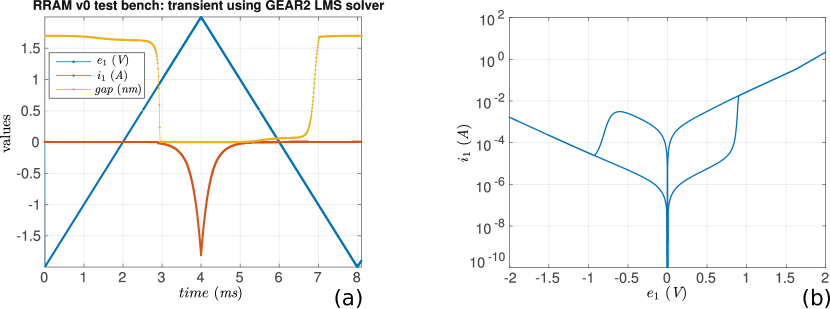
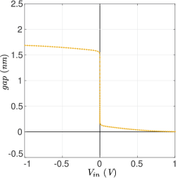
The model we develop also work in DC and homotopy analyses. - relationship under DC conditions acquired from homotopy analysis are shown in Fig. 7. DC sweeps from both directions in this case give the same results since the model doesn’t have DC hysteresis. The - curve in Fig. 7 matches our discussion on the solutions in Sec. IV-A.
Note that in the transient results, gap is not perfectly flat at or ; same phenomenon can also be observed in the DC solutions obtained using homotopy. This is because that the clipping functions we use, although fast growing, cannot set exact hard limits on the internal unknown. In other words, even when gap is close to or , changing the voltage can still affect gap slightly. This is not a modelling artifact. In fact, this makes the model numerically robust, and at the same time more physical. It maintains the smoothness of equations and reduces the chance for Jacobian matrix to become singular in simulation. Physically, even when is close to the boundary, changing voltage still causes the device’s state to change. The small changes in in this scenario can be interpreted as reflecting the change in device’s state, e.g., the width of the filament. We conclude that, by making the model equations smooth, we are actually making the model more physical.
V Convergence Aids
A common issue with newly-developed compact models of non-linear devices is that they often do not converge in simulation. In this section, we discuss several techniques in compact modelling that can often improve the convergence of simulation. Among these techniques, we focus on the use of SPICE-compatible limiting functions. We explain the intuition behind this technique and use this intuition to design a limiting function specific to the RRAM model.
In the previous sections, we have already discussed several convergence aiding techniques used in our RRAM model. One of them is the proper scaling of both unknowns and equations. This improves both the accuracy of solutions and the convergence of simulation. The use of GMIN makes sure that the two terminals are always connected with a finite resistance, reducing the chance for the circuit Jacobian matrix to become singular during simulation. We have also discussed the use of smooth and safe functions (smoothstep(), safeexp()). We highly recommend that compact model developers consider these techniques when they encounter convergence issues with their models.
However, the above techniques do not solve all the convergence problems with the RRAM model. In particular, we have observed that the values and derivatives of (12) and (13) often become very large while the Newton Raphson (NR) iterations [22] are trying different guesses during DC operating point analysis. This is because of the fast-growing sinh functions in the equations. One solution is to use safesinh instead of sinh. The safesinh function uses safeexp/limexp inside to eliminate the fast-growing part with its linearized version, keeping the function values from exploding numerically. Although it has some physical justifications, it also has the potential problems of inaccuracy, especially since the exponential relationship is the key to the switching behaviour of RRAM devices (Sec. IV-A). Therefore, in this section, we focus on another technique that can keep the fast-growing exp or sinh function intact, but prevent NR from evaluating these functions with large input values. The techniques are known as initialization and limiting; they were implemented in Berkeley SPICE, for nonlinear devices such as diodes, BJTs and MOSFETs. Initialization evaluates these fast-growing nonlinear equations of semiconductor devices with “good” voltage values at the first NR iteration; limiting changes the NR guesses for these voltages in the subsequent iterations, based on both the current guess at each iteration and the value used in the last evaluation.
The limiting functions in SPICE include pnjlim, fetlim and limvds. Among them, pnjlim calculates new p-n junction voltage based on the current NR guess and the last junction voltage being used, in an attempt to avoid evaluating the exp function in the diode equation with large values. This mechanism is applicable to sinh as well. Inspired by pnjlim, we design a sinhlim that can reduce the chance of numerical exposion for the RRAM model.
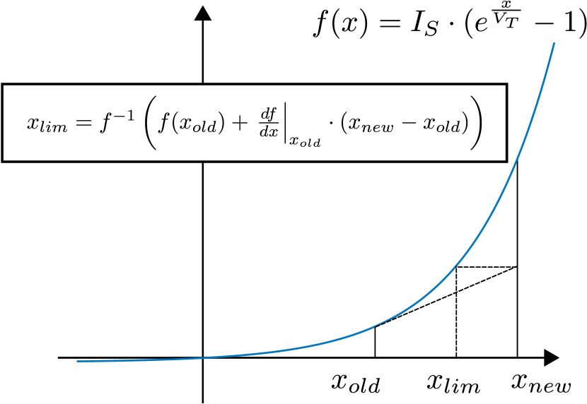
pnjlim calculates the new junction voltage using the mechanism illustrated in Fig. 9. The current NR guess is , which is too large a value for evaluating an exponential function. So pnjlim calculates the limited version, , in between and . Since NR linearized the system equation at in the last NR iteration, and the linearization indicates that the new guess is , what NR actually wants is for the p-n junction to generate the current predicted for . Because this prediction is based on the linearization at , the actual current at is apparently far larger than it. Therefore, a more sensible choice for the junction voltage should be one that gives out the predicted current. From the above discussion, we can write an equation for the desired :
| (23) |
Solving from the above equation, we get the core of pnjlim.
| (24) |
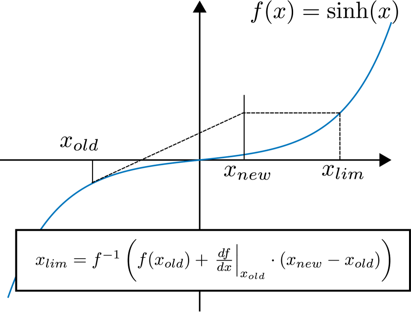
From the above formula, the operation of pnjlim is essentially inverting the diode I-V equation to calculate the desired voltage from the predicted current at . Based on the same idea, we can write the limiting function for sinh. As illustrated in Fig. 9, given and the current guess , we can calculate the desired “current” (function value), then invert sinh to get the corresponding for function evaluation. Such an satisfies
| (25) |
which gives out the formulation of sinhlim:
| (26) |
This new limiting function sinhlim can be easily implemented in any SPICE-compatible circuit simulator. To demonstrate its effectiveness, we implement a simple two-terminal device with its I-V relationship governed by a sinh function, i.e., the device equation is . As sinh is a rapidly-growing function, even a simple circuit with a series connection of a voltage source, a resistor of and this device may not converge if the supply voltage is large. This is because when searching for the solution, plain NR algorithm may try large voltage values as inputs to the model’s sinh function, resulting difficulties or failure in convergence. In contrast, SPICE-compatible NR can use sinhlim to calculate for use in iterations, preventing using large directly. We run DC operating point analyses on this simple circuit, with NR starting from all-zeros as initial guesses. As shown in Table I, with the same convergence criteria,161616In the simulation experiments, reltol is 1e-6, abstol is 1e-12, residualtol is 1e-12. the use of sinhlim improves convergence greatly.
| Supply Voltage (V) | with sinlim (niters) | without limiting (niters) |
|---|---|---|
| 1 | 4 | 4 |
| 10 | 4 | 9 |
| 100 | 4 | 50 |
| 1000 | 4 | non-convergence within 100 iters |
We implement parameterized versions of the sinhlim function in our RRAM model to aid convergence; the code is included in Appendix B-A. Since there are two sinh function used in the RRAM model, in both and , two limited variables are declared in the model, with two sinhlim with different parameters used in a vectorized limiting function.
Many simulators available today are SPICE-compatible, in the sense that they implement the equivalent limiting technique as in SPICE.171717Some simulators implement a technique known as “limiting correction”, which is compatible with SPICE’s limiting formulation. Our sinhlim can also be incorporated there. However, we would like to note that the limiting functions available in literature today, 40 years after the introduction of SPICE, are still limited to only the original pnjlim, fetlim and limvds. The sinhlim we have developed for RRAM models, is a new one. Moreover, among all these limiting functions, sinhlim is the only one that is smooth and continuous, making it more robust to use in simulation.
VI Models for General Memristive Devices
In this section, we apply the modelling techniques and methodology we have developed in previous sections to the modelling of general memristive devices. We use the same model template we have demonstrated in Sec. II, where specifies the device’s I-V relationship, describes the dynamics of the internal unknown. For general memristive devices, there are several equations available for and , from existing models such as the linear and non-linear ion drift models [31], Simmons tunnelling barrier model [50], TEAM/VTEAM model [34, 51], Yakopcic’s model [32, 33], etc. In this section, we examine the reason why they do not work well in simulation, especially in DC analysis. We first summarize the common issues with the and functions used in them, then examine the individual problems of each / function, and list our improvements in Table II and Table III.
As discussed earlier, both , the I-V relationship, and , the internal unknown dynamics, are often highly non-linear and asymmetric wrt positive and negative voltages; available and functions often use discontinuous and fast-growing components in them, e.g., exponential, sinh functions, power functions with a large exponent, etc. These components result in difficulty of convergence in simulation. To overcome these difficulties, similar to what we did in Sec. IV for the RRAM model, we can use smooth and safe functions.
The key idea of the design of smooth functions is to combine common elementary functions to approximate the original non-smooth ones. A parameter common to all these functions, aka. smoothing factor, is used to control the trade-off between better approximation and more smoothness, which is often synonymous to better convergence. Similar ideas apply to safe functions. For the fast-growing functions, their “safe” versions limit the maximum slope the functions can reach, then linearize the functions to keep the slopes constant beyond those points. For functions that are not defined for all real inputs, e.g., sqrt, log, etc., their “safe” versions clip the inputs using smoothclip such that these functions will never get invalid inputs.
Specifically, for the available and functions, the if-then-else statements can be replaced with smoothswitch. The exp and sinh functions can be replaced with safeexp and safesinh. The power functions, e.g., pow(a, b), can also be replaced with safeexp(b*safelog(a)).
We have implemented common smooth and safe functions in MAPP. For example, issuing “help smoothclip” within MAPP will display more information on the usage of smoothclip. For Verilog-A, we have implemented these smooth and safe functions as “analog functions”, listed them in a separate file in Appendix C-C for model developers to use conveniently.
The use of smooth and safe functions are more than numerical tricks, and they do not necessarily make models less physical. On the contrary, physical systems are usually smooth. For example, when switching the voltage of a two-terminal device across zero, the current should change continuously and smoothly. Therefore, compared with the original if-then-else statements, the smoothswitch version is likely to be closer to physical reality. The same applies to the safe functions we use in our models. For example, there are no perfect exponential relationships in physical reality. Even the growth rate of bacteria, which is often characterized as exponential in time, will saturate eventually. Another quantity often modelled using exponential functions is the current through a p-n junction. When the voltage indeed becomes large, the junction doesn’t really give out next to infinite current. Instead, other factors come into play — the temperature will become too high that the structure will melt. This is not considered when writing the exponential I-V relationship; the use of exponential function is not to capture the physics exactly, but more an approximation and simplification of physical reality. So the use of safeexp and safesinh is more than just a means to prevent numerical explosion, but also a fix to the original over-simplified models.
| No. | Original | Comments and improved |
|---|---|---|
| 1 |
Can have division-by-zero when .
We use then |
|
| 2 | We change exponential function to safeexp(). | |
| 3 | We change sinh to safesinh(), exponential function to safeexp(). | |
| 4 | We change sinh to safesinh(), then smooth the function. | |
| 5 | We express using : Then we change sinh to safesinh(), exponential function to safeexp(). |
One common problem with existing functions is the range of the internal unknown. We have discussed this problem in Sec. IV in the context of RRAM device models. The functions available either neglect this issue or use window functions to set the bounds for the internal unknown. From the discussion in Sec. IV, using window functions introduces modelling artifacts that limit the usage of the model to only transient simulation. To fix this problem, we apply the same modelling technique using clipping functions in our memristor models.
| No. | Original | Comments and improved |
|---|---|---|
| 1 | Linear ion drift model: |
No DC hysteresis. Doesn’t ensure .
We use the clipping technique to set bounds for . |
| 2 | Nonlinear ion drift model: |
No DC hysteresis. Doesn’t ensure .
We use the clipping technique to set bounds for . |
| 3 | Simmons tunnelling barrier model: where . |
No DC hysteresis. Doesn’t ensure . Contains fast-growing functions.
We change sinh to safesinh(), exponential function to safeexp(), then implement the smooth version of this if-then-else statement. We use the clipping technique to set bounds for . |
| 4 | VTEAM model: |
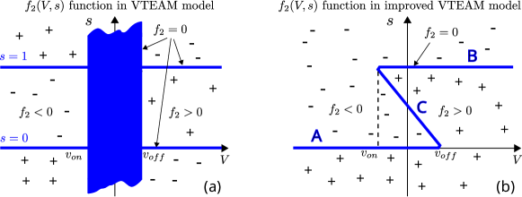
DC hysteresis is modelled by a flat region. We redesign the equation
based on Fig. 10.
where
such that when and , it is equivalent to VTEAM equation in the
and regions respectively.
We also make the function smooth: And finally, we use the clipping technique to set bounds for . |
| 5 | Yakopcic’s model: where and | DC hysteresis is modelled by a flat region. We redesign the equation based on Fig. 10. where We also change exponential function to safeexp(), make the function smooth, then use the clipping technique to set bounds for . |
| 6 | Standford/ASU RRAM model: where | We convert to : Then we change sinh to safesinh(), exponential function to safeexp(). We also use the clipping technique to set bounds for . |
Another problem with the available functions is the way they handle DC hysteresis. As discussed earlier, DC hysteresis is observed in forward and backward DC sweeps; it accounts for the pinched I-V curves when voltage is moving infinitely slow. From the model example hys_example in Sec. II, we can conclude that DC hysteresis results from the model’s DC solution curve folding backward in voltage, which creates multiple stable solutions of internal state variable at certain voltages. In fact, from the equations of TEAM/VTEAM model and Yakopcic’s model, we can see an attempt to model DC hysteresis. However, the way it is done in both these models is to set within a certain voltage range, e.g., when voltage is close to 0. In this way, as long as the voltage is within this range, there are infinitely many solutions for the model, regardless of values of . During transient simulation, will just keep its old value from the previous time point. In DC analysis, if also keeps its old value from the last sweeping point, there can be DC hysteresis. However, since actually has infinitely many solutions within this voltage range, the equation system becomes ill-conditioned. The circuit Jacobian matrix can also become singular, since has no control over the value of . Homotopy analysis won’t work with these device models since there is no solution curve to track. Even in DC operating point (OP) analysis, the OP can have a random as part of the solution, depending on the initial condition, and if it is not provided, on how the OP analysis is implemented. DC sweep results also depend on how DC sweep is written, particularly on the way the old values are used as initial guesses for current steps.181818For example, if the DC sweep implements predictor, when sweeping across the hysteresis range of voltage, may not stay flat. In other words, because of the model is ill-conditioned, the behaviour of the model is specific to the implementation of the analysis and will vary from simulator to simulator. To fix this problem, we modify the available functions such that the solutions form a single curve in state space, as illustrated in Fig. 10 (b). For each model, this requires different modifications specific to its equations; we list more detailed descriptions of these modifications in Table III.
To summarize the problems with existing memristor models and our solutions to them, we fix the nonsmoothness and overflow problems of the existing equations with smooth and safe functions; we fix the internal state boundry problem with the same clipping function technique we have used for the RRAM model; we fix the “flat” problem by properly implementing the curve that bends backward for the modelling of DC hysteresis. Table II and Table III list our approaches in improving the available and functions in more detail. The result is a collection of memristor models, controlled by two variables (which can be thought of as higher-level model parameters), f1_switch and f2_switch. All the combinations of 5 functions and 6 functions constitute 30 compact models for various types of memristors. Different and functions describe different underlying physics of the devices, with different levels of accuracy. We would like to note that one particular combination — f1_switch = 5, f2_switch = 6, is equivalent to the RRAM model we have discussed in Sec. IV.
Apart from this combination for RRAM devices, several other combinations in the general memristor model can also be used for RRAM devices. For example, when f2_switch =5 and f2_switch = 4, our proposed model uses the improved equations from the VTEAM and Yakopcic’s models. The range of the DC hysteresis in these models is controlled by two threshold voltages, e.g., and for Yakopcic’s model, and for VTEAM model. When both these two thresholds are equal to zero, the DC hysteresis disappears, and the models are suitable for RRAM devices. Also, when the two threshold voltages have the same sign, these models can also be used for unipolar memristive devices. They are more general and flexible than the model equations we have discussed in Sec. IV written only for bipolar RRAM devices. The ideas and techniques underlying these models are likely to also be applicable to new memristive devices and model equations to be developed in the future.
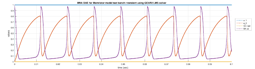
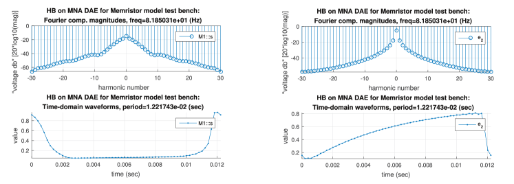
The ModSpec and Verilog-A files of the proposed general memristor models are listed in Appendix C-A and Appendix C-B respectively. They can be used in the same test benches for RRAMs in Sec. IV. Their parameters can also be fitted to generate similar results in Fig. 6 and Fig. 7. As an extra example, we use f1_switch=2, f2_switch=5, corresponding to the improved Yakopcic model, and adjust its parameters for a unipolar RRAM device, connect it with a resistor as shown in Fig. 12 to make an oscillator. Then we run both transient simulation and PSS analysis with Harmonic Balance and show their results in Fig. 12 and Fig. 13. These results demonstrate that our model not only run in DC, transient and homotopy analyses, but also work for PSS simulation.
VII Summary
Our study in this paper centers around the compact modelling of memristive devices. Memristor models available today do not work well in simulation, especially in DC analysis. Their problems come from several main sources. Firstly, some models are not in the differential equation format; they are essentially hybrid models with memory states used for hysteresis. We clarified that the proper modelling of hysteresis should be achieved through the use of an internal state variable and an implicit equation. To make this concept clear, we developed a model template and implemented an example, namely hys_example, in both ModSpec and Verilog-A. During this process, we examined the common mistakes model developers make when writing internal unknowns and implicit equations in the Verilog-A language. Then we applied the model template to model RRAM devices, which led to another common difficulty in memristor modelling — enforcing the upper and lower bounds of the internal unknown. We proposed numerical techniques with clipping functions that can modify the filament growth equation such that the bounds are respected in simulation. We also discussed the physical justification behind our approaches. Then we demonstrated that the same techniques can be applied to fix the similar problems with many other existing memristor models. As a result, we not only developed a suite of 30 memristor models, all tested to work with many simulation analyses in major simulators, but also took this process as an opportunity to identify and document many good and bad modelling practices. Both the resulting models and the techniques used in developing them should be valuable to the compact modelling community.
References
- [1] L.O. Chua. Memristor-the missing circuit element. IEEE Transactions on Circuit Theory, 18(5):507–519, 1971.
- [2] S.R. Williams. How We Found The Missing Memristor. IEEE Spectrum, 45(12):28–35, December 2008.
- [3] D.B. Strukov, G.S. Snider, D.R. Stewart and R.S. Williams. The missing memristor found. Nature, 453(7191):80–83, 2008.
- [4] S.H. Jo, K.-H. Kim and W. Lu. High-density crossbar arrays based on a Si memristive system. Nano letters, 9(2):870–874, 2009.
- [5] H.S. Yoon, I.-G. Baek, J. Zhao, H. Sim, M.Y. Park, H. Lee, G.-H. Oh and others. Vertical cross-point resistance change memory for ultra-high density non-volatile memory applications. In Symposium on VLSI Technology (VLSI Technology), June 2009.
- [6] S. Thakoor, A. Moopenn, T. Daud and A.P. Thakoor. Solid-state thin-film memistor for electronic neural networks. Journal of Applied Physics, 67(6):3132–3135, 1990.
- [7] F.A. Buot and A.K. Rajagopal. Binary information storage at zero bias in quantum-well diodes. Journal of Applied Physics, 76(9):5552–5560, 1994.
- [8] V. Erokhin and M.P. Fontana. Electrochemically controlled polymeric device: a memristor (and more) found two years ago. arXiv preprint arXiv:0807.0333, 2008.
- [9] H.-S. P. Wong, H.-Y. Lee, S. Yu, Y.-S. Chen, Y. Wu, P.-S. Chen, B. Lee, F.-T. Chen, and M.-J. Tsai. Metal-oxide RRAM. Proceedings of the IEEE, 100(6):1951–1970, 2012.
- [10] M. Kund, G. Beitel, C.-U. Pinnow, T. Rohr, J. Schumann, R. Symanczyk, K.-D. Ufert and G. Muller. Conductive bridging RAM (CBRAM): An emerging non-volatile memory technology scalable to sub 20nm. In Proc. IEEE IEDM, 2005.
- [11] A. Mehonic, S. Cueff, M. Wojdak, S. Hudziak, O. Jambois, C. Labbe, B. Garrido, R. Rizk and A.J. Kenyon. Resistive switching in silicon suboxide films. Journal of Applied Physics, 111(7):074507, April 2012.
- [12] J. Yang, D.B. Strukov and D.R. Stewart. Memristive devices for computing. Nature Nanotechnology, 8(1):13–24, 2013.
- [13] I. Vourkas and G.C. Sirakoulis. Memristor-Based Nanoelectronic Computing Circuits and Architectures. Springer, 2015.
- [14] E. Linn, R. Rosezin, C. Kügeler and R. Waser. Complementary resistive switches for passive nanocrossbar memories. Nature Materials, 9(5):403–406, 2010.
- [15] S.-S. Sheu, P.-C. Chiang, W.-P. Lin, H.-Y. Lee, P.-S. Chen, Y.-S. Chen, T.-Y. Wu, F. T. Chen, K.-L. Su and others. A 5ns fast write multi-level non-volatile 1 K bits RRAM memory with advance write scheme. In Symposium on VLSI Circuits, pages 82–83. IEEE, 2009.
- [16] F. Alibart, E. Zamanidoost and D.B. Strukov. Pattern classification by memristive crossbar circuits using ex situ and in situ training. Nature Communications, 4, 2013.
- [17] M. Sharad, D. Fan, K. Aitken and K. Roy. Energy-efficient non-boolean computing with spin neurons and resistive memory. IEEE Transactions on Nanotechnology, 13(1):23–34, 2014.
- [18] S.H. Jo, T. Chang, I. Ebong, B.B. Bhadviya, P. Mazumder and W. Lu. Nanoscale memristor device as synapse in neuromorphic systems. Nano Letters, 10(4):1297–1301, 2010.
- [19] Jacques Hadamard. Sur les problèmes aux dérivées partielles et leur signification physique. Princeton university bulletin, 13(49-52):28, 1902.
- [20] Sybil P Parker. McGraw-Hill Dictionary of Scientific and Technical Terms. McGraw-Hill Book Co., 1989.
- [21] W.H. Press, S.A. Teukolsky, W.T. Vetterling, and B.P. Flannery. Numerical Recipes – The Art of Scientific Computing. Cambridge University Press, 1989.
- [22] J. Roychowdhury. Numerical simulation and modelling of electronic and biochemical systems. Foundations and Trends in Electronic Design Automation, 3(2-3):97–303, December 2009.
- [23] T. Wang and J. Roychowdhury. Guidelines for Writing NEEDS-compatible Verilog-A Compact Models. https://nanohub.org/resources/18621, Jun 2013.
- [24] L. A. Zadeh and C. A. Desoer. Linear System Theory: The State-Space Approach. McGraw-Hill Series in System Science. McGraw-Hill, New York, 1963.
- [25] P. Sheridan, K.-H. Kim, S. Gaba, T. Chang, L. Chen and W. Lu. Device and SPICE modeling of RRAM devices. Nanoscale, 3(9):3833–3840, 2011.
- [26] X. Guan, S. Yu and H.-S. P. Wong. A SPICE compact model of metal oxide resistive switching memory with variations. IEEE electron device letters, 33(10):1405–1407, 2012.
- [27] Z. Jiang, S. Yu, Y. Wu, J.H. Engel, X. Guan and H.-S. P. Wong. Verilog-A compact model for oxide-based resistive random access memory (RRAM). In International Conference on Simulation of Semiconductor Processes and Devices (SISPAD), pages 41–44. IEEE, 2014.
- [28] H. Li, Z. Jiang, P. Huang, Y. Wu, H.-Y. Chen, B. Gao, X.Y. Liu, J.F. Kang and H.-S. P. Wong. Variation-aware, reliability-emphasized design and optimization of RRAM using SPICE model. In Proc. IEEE DATE, pages 1425–1430. EDA Consortium, 2015.
- [29] P.-Y. Chen and S. Yu. Compact Modeling of RRAM Devices and Its Applications in 1T1R and 1S1R Array Design. IEEE Transactions on Electron Devices, 62(12):4022–4028, 2015.
- [30] K. Xu, Y. Zhang, L. Wang, M. Yuan, Y. Fan, W. Joines and Q. Liu. Two memristor SPICE models and their applications in microwave devices. IEEE Transactions on Nanotechnology, 13(3):607–616, 2014.
- [31] S. Kvatinsky, K. Talisveyberg, D. Fliter, E.G. Friedman, A. Kolodny and U.C. Weiser. Verilog-A for memristors models. In CCIT Tech. Rep. 801, 2011.
- [32] C. Yakopcic, T.M. Taha, G. Subramanyam and R.E. Pino. Generalized memristive device SPICE model and its application in circuit design. IEEE Trans. CAD, 32(8):1201–1214, 2013.
- [33] C. Yakopcic. Memristor Device Modeling and Circuit Design for Read Out Integrated Circuits, Memory Architectures, and Neuromorphic Systems. PhD thesis, University of Dayton, 2014.
- [34] S. Kvatinsky, E.G. Friedman, A. Kolodny and U.C. Weiser. TEAM: threshold adaptive memristor model. IEEE Trans. on Circuits and Systems I: Fundamental Theory and Applications, 60(1):211–221, 2013.
- [35] L. Lemaitre, G. Coram, C. C. McAndrew, and K. Kundert. Extensions to Verilog-A to support compact device modeling. In Behavioral Modeling and Simulation, 2003. BMAS 2003. Proceedings of the 2003 International Workshop on, pages 134–138. IEEE, 2003.
- [36] G. Coram. How to (and how not to) write a compact model in Verilog-A. In Behavioral Modeling and Simulation, 2004. BMAS 2004. Proceedings of the 2004 International Workshop on, pages 97–106. IEEE, 2004.
- [37] C.C. McAndrew, G.J. Coram, K.K. Gullapalli, J.R. Jones, L.W. Nagel, A.S. Roy, J. Roychowdhury, A.J. Scholten, Geert D.J. Smit, X. Wang and S. Yoshitomi. Best Practices for Compact Modeling in Verilog-A. IEEE J. Electron Dev. Soc., 3(5):383–396, September 2015.
- [38] D. Amsallem and J. Roychowdhury. ModSpec: An open, flexible specification framework for multi-domain device modelling. In Computer-Aided Design (ICCAD), 2011 IEEE/ACM International Conference on, pages 367–374. IEEE, 2011.
- [39] T. Wang, K. Aadithya, B. Wu, J. Yao, and J. Roychowdhury. MAPP: The Berkeley Model and Algorithm Prototyping Platform. In Proc. IEEE CICC, pages 461–464, September 2015. DOI link.
- [40] J. Roychowdhury and R. Melville. Delivering Global DC Convergence for Large Mixed-Signal Circuits via Homotopy/Continuation Methods. IEEE Trans. CAD, 25:66–78, Jan 2006.
- [41] L.W. Nagel. SPICE2: a computer program to simulate semiconductor circuits. PhD thesis, EECS department, University of California, Berkeley, Electronics Research Laboratory, 1975. Memorandum no. ERL-M520.
- [42] L.O. Chua and S.M. Kang. Memristive devices and systems. Proceedings of the IEEE, 64(2):209–223, 1976.
- [43] S. Lin, L. Zhao, J. Zhang, H. Wu, Y. Wang, H. Qian and Z. Yu. Electrochemical simulation of filament growth and dissolution in conductive-bridging RAM (CBRAM) with cylindrical coordinates. In Proc. IEEE IEDM, 2012.
- [44] MAPP: The Berkeley Model and Algorithm Prototyping Platform. Web site: http://mapp.eecs.berkeley.edu.
- [45] J. McPherson, J. Kim-Y., A. Shanware and H. Mogul. Thermochemical description of dielectric breakdown in high dielectric constant materials. Applied Physics Letters, 82:2121, 2003.
- [46] Z. Fang H. Yu J. Kang S. Yu, B. Gao and H.-S. P. Wong. A neuromorphic visual system using RRAM synaptic devices with Sub-pJ energy and tolerance to variability: Experimental characterization and large-scale modeling. In Proc. IEEE IEDM, pages 10–4. IEEE, 2012.
- [47] P. Meuffels and R. Soni. Fundamental issues and problems in the realization of memristors. arXiv:1207.7319, 2012.
- [48] M. Di Ventra and Y.V. Pershin. On the physical properties of memristive, memcapacitive and meminductive systems. Nanotechnology, 24(25):255201, 2013.
- [49] V.A. Slipko, Y.V. Pershin and M. Di Ventra. Changing the state of a memristive system with white noise. Physical Review E, 87(4):042103, 2013.
- [50] Pickett, M. and Strukov, D. and Borghetti, J. and Yang, J. and Snider, G. and Stewart, D. and Williams, S. Switching dynamics in titanium dioxide memristive devices. Journal of Applied Physics, 106(7):074508, 2009.
- [51] S. Kvatinsky, M. Ramadan, E. Friedman and A. Kolodny. VTEAM: A General Model for Voltage-Controlled Memristors. IEEE Trans. on Circuits and Systems II: Analog and Digital Signal Processing, 62(8):786–790, 2015.
Appendix A Model and Circuit Code for hys — A Device Example with Hysteresis
A-A hys_ModSpec.m: model file for hys in MAPP
-
1function MOD = hys_ModSpec()2 MOD = ee_model();3 MOD = add_to_ee_model(MOD, ’name’, ’hys’);4 MOD = add_to_ee_model(MOD, ’terminals’, {’p’, ’n’}); % create IO: vpn, ipn5 MOD = add_to_ee_model(MOD, ’explicit_outs’, {’ipn’});6 MOD = add_to_ee_model(MOD, ’internal_unks’, {’s’});7 MOD = add_to_ee_model(MOD, ’implicit_eqn_names’, {’ds’});8 MOD = add_to_ee_model(MOD, ’parms’, {’R’, 1e3, ’k’, 1, ’tau’, 1e-5});9 MOD = add_to_ee_model(MOD, ’fqei’, {@fe, @qe, @fi, @qi});10 MOD = finish_ee_model(MOD);11end % hys_ModSpec1213function out = fe(S)14 v2struct(S); % populates workspace with vpn, R, k, tau15 out = vpn/R * (1+tanh(k*s)); % ipn16end % fe1718function out = qe(S)19 out = 0; % ipn20end % qe2122function out = fi(S)23 v2struct(S);24 out = vpn - s^3 + s;25end % fi2627function out = qi(S)28 v2struct(S);29 out = - tau * s;30end % qi
Listing 1: hys_ModSpec.m
A-B hys.va: Verilog-A model for hys
-
1// A device with hysteresis2‘include "disciplines.vams"34module hys(p, n);5 inout p, n;6 electrical p, n, ns;7 parameter real R = 1e3 from (0:inf);8 parameter real k = 1 from (0:inf);9 parameter real tau = 1e-5 from (0:inf);10 real s;1112 analog begin13 s = V(ns, n);14 I(p, n) <+ V(p, n)/R * (1+tanh(k*s));15 I(ns, n) <+ V(p, n) - pow(s, 3) + s;16 I(ns, n) <+ ddt(-tau*s);17 end18endmodule
Listing 2: hys.va
A-C test_hys.m: circuit and test script for hys in MAPP
-
1clear ckt;2ckt.cktname = ’hys_ckt’;3ckt.nodenames = {’1’};4ckt.groundnodename = ’gnd’;5mysinfunc = @(t, args) 0.7 * sin(2*pi*1e3*t);6ckt = add_element(ckt, vsrcModSpec(), ’V1’, ...7 {’1’, ’gnd’}, {}, {{’DC’, 0}, {’TRAN’, mysinfunc, []}});8ckt = add_element(ckt, hys_ModSpec(), ’H1’, {’1’, ’gnd’});910% create DAE11DAE = MNA_EqnEngine(ckt);1213% forward DC sweep14swp1 = dcsweep(DAE, [], ’V1:::E’, -1:0.015:1);15[pts1, sols1] = swp1.getSolution(swp1);16figure; plot(pts1(1,:), -sols1(2,:), ’.-r’); drawnow; % V1::ipn1718% backward DC sweep19swp2 = dcsweep(DAE, [], ’V1:::E’, 1:-0.015:-1);20[pts2, sols2] = swp2.getSolution(swp2);21hold on; plot(pts2(1,:), -sols2(2,:), ’.-b’); drawnow; % V1::ipn2223% run transient simulation24tran = dot_transient(DAE, [], 0, 5e-6, 2.5e-3);25[tpts, sols] = tran.getSolution(tran);2627% plot transient28hold on; plot(sols(1,:), -sols(2,:), ’.-k’); % e_1, V1::ipn29xlabel(’V1:::E (V)’); ylabel(’-V1:::ipn (A)’); grid on;30legend(’forward DC sweep’, ’backward DC sweep’, ’transient’);3132figure; plot(pts1(1,:), sols1(3,:), ’.-r’); % H1:::s33hold on; plot(pts2(1,:), sols2(3,:), ’.-b’); % H1:::s34hold on; plot(sols(1,:), sols(3,:), ’.-k’); % H1:::s35legend(’forward DC sweep’, ’backward DC sweep’, ’transient’);36xlabel(’V1:::E (V)’); ylabel(’H1:::s’); grid on;3738% run homotopy analysis39startLambda = -1; stopLambda = 1; lambdaStep = 1e-1; initguess = [-1;0;-1];40hom = homotopy(DAE, ’V1:::E’, ’input’, initguess, startLambda, lambdaStep, stopLambda);41hom.plot(hom);4243souts = StateOutputs(DAE); souts = souts.DeleteAll(souts);44souts = souts.Add({’V1:::ipn’}, souts); hom.plot(hom, souts);4546sols = hom.getsolution(hom);47figure; plot3(sols.yvals(1,:), sols.yvals(2,:), sols.yvals(3,:));48unk_names = DAE.unknames(DAE);49xlabel(unk_names{1}); ylabel(unk_names{2}); zlabel(unk_names{3});50grid on; box on;
Listing 3: test_hys.m
A-D test_hys.cir: circuit and test script for hys in Xyce
-
1* test hys.va in DC, TRAN and Homotopy23V1 1 0 1 sin(0 0.7 1k)4Yhys H1 1 056* DC analysis7* .dc V1 -1 1 0.0189* transient simulation10* .tran 1u 2m11* .print tran V(1) I(V1) N(Yhys!H1_ns)1213* homotopy analysis14.dc V1 .7 .7 115.print homotopy V(1) I(V1) N(Yhys!H1_ns)16.options nonlin continuation=117.options loca stepper=ARC18+ predictor=1 stepcontrol=119+ conparam=V1:DCV020+ initialvalue=-1.0 minvalue=-1.0 maxvalue=1.021+ initialstepsize=0.01 minstepsize=1.0e-8 maxstepsize=0.122+ aggressiveness=0.1
Listing 4: test_hys.cir
A-E test_hys.scs: circuit and test script for hys in Spectre
-
1simulator lang=spectre23ahdl_include "hys.va"45V1 (1 0) vsource dc=1 type=sine sinedc=0 ampl=0.7 freq=1k6X1 (1 0) hys78// DC analysis9dc1 dc dev=V1 start=-1 stop=1 lin=10010dc2 dc dev=V1 start=1 stop=-1 lin=1001112// transient simulation13tran tran stop=2m
Listing 5: test_hys.scs
A-F test_hys.sp: circuit and test script for hys in HSPICE
-
1* test hys.va in DC, and TRAN2.OPTION POST3.hdl hys.va4V1 1 0 1 sin(0 0.7 1k)5X1 1 0 hys67* DC analysis8.dc V1 -1 +1 0.01910* transient simulation11.tran 1u 2m12.end
Listing 6: test_hys.sp
Appendix B Model and Circuit Code for RRAM version 0
B-A RRAM_v0_ModSpec.m: model file for RRAM version 0 in MAPP
-
1function MOD = RRAM_v0_ModSpec()2 MOD = ee_model();3 MOD = add_to_ee_model(MOD, ’name’, ’RRAM’);4 MOD = add_to_ee_model(MOD, ’terminals’, {’t’, ’b’}); % create IO: vtb, itb5 MOD = add_to_ee_model(MOD, ’explicit_outs’, {’itb’});6 MOD = add_to_ee_model(MOD, ’internal_unks’, {’Gap’});7 MOD = add_to_ee_model(MOD, ’implicit_eqn_names’, {’dGap’});89 MOD = add_to_ee_model(MOD, ’parms’, {’g0’, 0.25, ’V0’, 0.25, ’I0’, 1e-3});10 MOD = add_to_ee_model(MOD, ’parms’, {’Vel0’, 10, ’Beta’, 0.8, ’gamma0’, 16});11 MOD = add_to_ee_model(MOD, ’parms’, {’Ea’, 0.6, ’a0’, 0.25, ’tox’, 12});12 MOD = add_to_ee_model(MOD, ’parms’, {’maxGap’, 1.7, ’minGap’, 0});13 MOD = add_to_ee_model(MOD, ’parms’, {’maxslope’, 1e15});14 MOD = add_to_ee_model(MOD, ’parms’, {’smoothing’, 1e-8, ’Kclip’, 50});15 MOD = add_to_ee_model(MOD, ’parms’, {’GMIN’, 1e-12});1617 MOD = add_to_ee_model(MOD, ’fqei’, {@fe, @qe, @fi, @qi});1819 MOD = add_to_ee_model(MOD, ’limited_var’, {’vtblim1’, ’vtblim2’});20 MOD = add_to_ee_model(MOD, ’limited_matrix’, [1, 0; 1, 0]);21 MOD = add_to_ee_model(MOD, ’limiting’, @limiting);22 MOD = add_to_ee_model(MOD, ’initGuess’, @initGuess);2324 MOD = finish_ee_model(MOD);25end2627function out = fe(S)28 v2struct(S);29 out = I0*safeexp(-Gap/g0, maxslope)*sinh(vtblim1/V0) + GMIN*vtb; % itb30end3132function out = qe(S)33 out = 0; % itb34end3536function out = fi(S)37 v2struct(S);38 T = 300;39 k = 1.3806226e-23; % Boltzmann’s Constant (joules/kelvin)40 q = 1.6021918e-19; % Electron Charge (C)4142 Gamma = gamma0 - Beta * Gap^3;43 ddt_Gap = - Vel0 * exp(- q*Ea/k/T) * sinh(vtblim2 * Gamma*a0/tox*q/k/T);4445 Fw1 = smoothstep(minGap-Gap, smoothing);46 Fw2 = smoothstep(Gap-maxGap, smoothing);47 clip_minGap = (safeexp(Kclip*(minGap-Gap), maxslope) - ddt_Gap) * Fw1;48 clip_maxGap = (-safeexp(Kclip*(Gap-maxGap), maxslope) - ddt_Gap) * Fw2;4950 out = ddt_Gap + clip_minGap + clip_maxGap;51end5253function out = qi(S)54 v2struct(S);55 out = - 1e-9 * Gap;56end5758function vtblimInitout = initGuess(S)59 v2struct(S);60 vtblimInitout(1, 1) = 0;61 vtblimInitout(2, 1) = 0;62end6364function vtblimout = limiting(S)65 v2struct(S);66 T = 300;67 k = 1.3806226e-23; % Boltzmann’s Constant (joules/kelvin)68 q = 1.6021918e-19; % Electron Charge (C)69 vtblimout(1, 1) = sinhlim(vtb, vtblim1, 1/V0);70 Gamma = gamma0 - Beta * Gap^3;71 vtblimout(2, 1) = sinhlim(vtb, vtblim2, Gamma*a0/tox*q/k/T);72end7374function xlim = sinhlim(x, xold, k)75 % return xlim such that sinh(k*xlim) = sinh(k*xold) + k*cosh(k*xold) * (x - xold)76 ylim = sinh(k*xold) + k*cosh(k*xold) * (x - xold);77 xlim = log(ylim + sqrt(1+ylim^2)) / k;78end
Listing 7: RRAM_v0_ModSpec.m
B-B RRAM_v0.va: Verilog-A model for RRAM version 0
-
1‘include "disciplines.vams"2‘include "constants.vams"3module RRAM_v0(t, b);4 inout t, b;5 electrical t, b, nGap;6 parameter real g0 = 0.25 from (0:inf);7 parameter real V0 = 0.25 from (0:inf);8 parameter real Vel0 = 10 from (0:inf);9 parameter real I0 = 1e-3 from (0:inf);10 parameter real Beta = 0.8 from (0:inf);11 parameter real gamma0 = 16 from (0:inf);12 parameter real Ea = 0.6 from (0:inf);13 parameter real a0 = 0.25 from (0:inf);14 parameter real tox = 12 from (0:inf);1516 parameter real maxGap = 1.7 from (0:inf);17 parameter real minGap = 0.0 from (0:inf);1819 parameter real smoothing = 1e-8 from (0:inf);20 parameter real GMIN = 1e-12 from (0:inf);21 parameter real Kclip = 50 from (0:inf);2223 real Gap, ddt_gap, Gamma, Fw1, Fw2, clip_0, clip_maxGap;2425 analog function real smoothstep;26 input x, smoothing;27 real x, smoothing;28 begin29 smoothstep = 0.5*(x/sqrt(x*x + smoothing)+1);30 end31 endfunction // smoothstep3233 analog begin34 Gap = V(nGap, b);35 I(t, b) <+ I0 * limexp(-Gap/g0) * sinh(V(t, b)/V0) + GMIN*V(t, b);3637 Gamma = gamma0 - Beta * pow(Gap, 3);38 ddt_gap = -Vel0*exp(-Ea/$vt)*sinh(V(t, b)*Gamma*a0/tox/$vt);3940 Fw1 = smoothstep(minGap-Gap, smoothing);41 Fw2 = smoothstep(Gap-maxGap, smoothing);42 clip_minGap = (limexp(Kclip*(minGap-Gap)) - ddt_gap) * Fw1;43 clip_maxGap = (-limexp(Kclip*(Gap-maxGap)) - ddt_gap) * Fw2;4445 I(nGap, b) <+ ddt_gap + clip_minGap + clip_maxGap;46 I(nGap, b) <+ ddt(-1e-9*Gap);47 end48endmodule
Listing 8: RRAM_v0.va
B-C test_RRAM_v0.m: circuit and test script for RRAM version 0 in MAPP
-
1clear ckt;2ckt.cktname = ’RRAM v0 test bench’;3ckt.nodenames = {’in’};4ckt.groundnodename = ’gnd’;5tranfunc = @(t, args) args.offset+args.A*sawtooth(2*pi/args.T*t+args.phi, 0.5);6tranargs.offset = 0; tranargs.A = 2; tranargs.T = 8e-3; tranargs.phi=0;7ckt = add_element(ckt, vsrcModSpec(), ’Vin’, ...8 {’in’, ’gnd’}, {}, {{’DC’, 1}, {’TRAN’, tranfunc, tranargs}});9ckt = add_element(ckt, RRAM_v0_ModSpec(), ’R1’, {’in’, ’gnd’}, {});1011% set up DAE12DAE = MNA_EqnEngine(ckt);1314% DC OP analysis15dcop = dot_op(DAE);16dcop.print(dcop); dcSol = dcop.getSolution(dcop);1718% transient simulation, sweep Vin19tstart = 0; tstep = 1e-5; tstop = 8e-3;20xinit = [0; 0; 1.7];21LMSobj = dot_transient(DAE, xinit, tstart, tstep, tstop);22LMSobj.plot(LMSobj);2324% get transient data, plot current in log scale25[tpts, sols] = LMSobj.getSolution(LMSobj);26figure; semilogy(sols(1,:), abs(sols(2,:)));27xlabel(’Vin (V)’); ylabel(’log(current) (A)’); grid on;2829% homotopy analysis30startLambda = 1; stopLambda = -1; lambdaStep = -1e-1;31hom = homotopy(DAE, ’Vin:::E’, ’input’, dcSol, startLambda, lambdaStep, stopLambda);32hom.plot(hom);
Listing 9: test_RRAM_v0.m
B-D test_RRAM_v0.cir: circuit and test script for RRAM version 0 in Xyce
-
1* test RRAM_v0.va in DC, TRAN23Vin in 0 DC -1 pulse(-1 1 1u 4m 4m 1u 8m)4YRRAM_v0 X1 in 056* DC analysis7* .dc Vin -1 1 0.0189* transient simulation10.tran 1u 8m
Listing 10: test_RRAM_v0.cir
B-E test_RRAM_v0.scs: circuit and test script for RRAM version 0 in Spectre
-
1simulator lang=spectre23ahdl_include "RRAM_v0.va"45Vin (in 0) vsource type=pulse val0=-1 val1=1 delay=1u rise=4m fall=4m width=1u period=8m+2u6X1 (in 0) RRAM_v078// DC analysis9dc dc dev=Vin start=-1 stop=1 lin=1001011// transient simulation12tran tran stop=8m
Listing 11: test_RRAM_v0.scs
B-F test_RRAM_v0.sp: circuit and test script for RRAM version 0 in HSPICE
-
1* circuit with one voltage source and one RRAM2.OPTION POST3.hdl RRAM_v0.va4Vin in 0 DC -1 pulse(-1 1 1u 4m 4m 1u 8m)5X1 in 0 RRAM_v06.dc Vin -1 1 0.017.tran 1e-6 8m8.end
Listing 12: test_RRAM_v0.sp
Appendix C Model Code for Memristor
C-A Memristor.m: model file for memristor ModSpec model in MAPP
-
1function MOD = Memristor(f1_switch, f2_switch)2 default_f1_switch = 1;3 default_f2_switch = 4;4 if nargin < 25 f2_switch = default_f2_switch;6 if nargin < 17 f1_switch = default_f1_switch;8 end9 end1011 MOD = ee_model();12 MOD = add_to_ee_model(MOD, ’name’, ’Memristor’);13 MOD = add_to_ee_model(MOD, ’terminals’, {’p’, ’n’}); % create IO: vpn, ipn14 MOD = add_to_ee_model(MOD, ’explicit_outs’, {’ipn’});15 MOD = add_to_ee_model(MOD, ’internal_unks’, {’s’});16 MOD = add_to_ee_model(MOD, ’implicit_eqn_names’, {’ds’});1718 MOD = add_to_ee_model(MOD, ’parms’, {’f1_switch’, f1_switch, ’f2_switch’, f2_switch});19 switch f1_switch20 case 121 MOD = add_to_ee_model(MOD, ’parms’, {’Ron’, 20, ’Roff’, 2e4});22 case 223 MOD = add_to_ee_model(MOD, ’parms’, {’Lambda’, 6.91, ’Ron’, 20});24 case 325 MOD = add_to_ee_model(MOD, ’parms’, {’n’, 3, ’Beta’, 1e-2, ’Alpha’, 2});26 MOD = add_to_ee_model(MOD, ’parms’, {’chi’, 1e-6, ’Gamma’, 4});27 case 428 MOD = add_to_ee_model(MOD, ’parms’, {’A1’, 1e-2, ’A2’, 1e-2, ’B’, 2});29 case 530 MOD = add_to_ee_model(MOD, ’parms’, {’g0’, 0.25, ’V0’, 0.25, ’I0’, 1e-3});31 MOD = add_to_ee_model(MOD, ’parms’, {’maxGap’, 1.7, ’minGap’, 0});32 otherwise33 end3435 switch f2_switch36 case 137 MOD = add_to_ee_model(MOD, ’parms’, {’mu_v’, 1e6});38 if 1 ~= f1_switch && 2 ~= f1_switch39 MOD = add_to_ee_model(MOD, ’parms’, {’Ron’, 20});40 end41 case 242 MOD = add_to_ee_model(MOD, ’parms’, {’a’, 1e4, ’m’, 3});43 case 344 MOD = add_to_ee_model(MOD, ’parms’, {’c_off’, 1e5, ’c_on’, 1e5});45 MOD = add_to_ee_model(MOD, ’parms’, {’i_off’, 1e-2, ’i_on’, 1e-2});46 MOD = add_to_ee_model(MOD, ’parms’, {’a_off’, 0.6, ’a_on’, 0.4});47 MOD = add_to_ee_model(MOD, ’parms’, {’wc’, 1e3, ’b’, 1});48 case 449 MOD = add_to_ee_model(MOD, ’parms’, {’k_off’, 50, ’k_on’, -50});50 MOD = add_to_ee_model(MOD, ’parms’, {’v_off’, 0.2, ’v_on’, -0.2});51 MOD = add_to_ee_model(MOD, ’parms’, {’alpha_off’, 3, ’alpha_on’, 3});52 case 553 MOD = add_to_ee_model(MOD, ’parms’, {’Vp’, 0.16, ’Vn’, 0.15, ’Ap’, 4e3, ’An’, 4e3});54 MOD = add_to_ee_model(MOD, ’parms’, {’xp’, 0.3, ’xn’, 0.5, ’alphap’, 1, ’alphan’, 5});55 case 656 if 5 ~= f1_switch57 MOD = add_to_ee_model(MOD, ’parms’, {’maxGap’, 1.7, ’minGap’, 0});58 end59 MOD = add_to_ee_model(MOD, ’parms’, {’Vel0’, 10, ’Beta0’, 0.8, ’gamma0’, 16});60 MOD = add_to_ee_model(MOD, ’parms’, {’Ea’, 0.6, ’a0’, 0.25, ’tox’, 12});61 otherwise62 end6364 MOD = add_to_ee_model(MOD, ’parms’, {’maxslope’, 1e15});65 MOD = add_to_ee_model(MOD, ’parms’, {’smoothing’, 1e-8, ’Kclip’, 50});66 MOD = add_to_ee_model(MOD, ’parms’, {’GMIN’, 1e-12});6768 MOD = add_to_ee_model(MOD, ’fqei’, {@fe, @qe, @fi, @qi});6970 MOD = finish_ee_model(MOD);71end7273function out = fe(S)74 v2struct(S);7576 switch f1_switch77 case 178 y = smoothclip(s - Roff/(Ron-Roff), smoothing) + Roff/(Ron-Roff);79 f1 = vpn / (Ron*y + Roff*(1-y));80 case 281 f1 = 1/Ron * safeexp(-Lambda * (1-s), maxslope) * vpn;82 case 383 f1 = s^n*Beta*safesinh(Alpha*vpn, maxslope) + chi*(safeexp(Gamma*vpn, maxslope)-1);84 case 485 f1p = A1 * s * safesinh(B * vpn, maxslope);86 f1n = A2 * s * safesinh(B * vpn, maxslope);87 f1 = smoothswitch(f1n, f1p, vpn, smoothing);88 case 589 f1 = I0*safeexp(-(s*minGap+(1-s)*maxGap)/g0, maxslope)*safesinh(vpn/V0, maxslope);90 otherwise91 end9293 out = f1 + GMIN*vpn; % ipn94end9596function out = qe(S)97 out = 0; % ipn98end99100function out = fi(S)101 v2struct(S);102103 switch f2_switch104 case 1105 f2 = mu_v * Ron * fe(S);106 case 2107 f2 = a * (vpn)^m;108 case 3109 i = fe(S);110 f2p = c_off * safesinh(i/i_off, maxslope) * ...111 safeexp(-safeexp((s-a_off)/wc - i/b, maxslope) - s/wc, maxslope);112 f2n = c_on * safesinh(i/i_on, maxslope) * ...113 safeexp(-safeexp(-(s-a_on)/wc + i/b, maxslope) - s/wc, maxslope);114 f2 = smoothswitch(f2n, f2p, i, smoothing);115 case 4116 Vstar = vpn-v_off+(v_off-v_on)*s;117 f2p = k_off * (Vstar/v_off)^alpha_off;118 f2n = k_on * (Vstar/v_on)^alpha_on;119 f2 = smoothswitch(f2n, f2p, Vstar, smoothing);120 case 5121 Vstar = vpn - (-Vn*s + Vp*(1-s));122 g_of_vpnp = Ap * (safeexp(vpn, maxslope) - safeexp(-Vn*s + Vp*(1-s), maxslope));123 g_of_vpnn = -An * (safeexp(-vpn, maxslope) - safeexp(+Vn*s - Vp*(1-s), maxslope));124 g_of_vpn = smoothswitch(g_of_vpnn, g_of_vpnp, Vstar, smoothing);125126 f_of_sp = smoothswitch(1, safeexp(-alphap*(s-xp), maxslope), s-xp, smoothing);127 f_of_s = smoothswitch(safeexp(alphan*(s-1+xn), maxslope), f_of_sp, s-1+xn, smoothing);128129 f2 = g_of_vpn * f_of_s;130 case 6131 T = 300;132 k = 1.3806226e-23; % Boltzmann’s Constant (joules/kelvin)133 q = 1.6021918e-19; % Electron Charge (C)134135 Gap = s*minGap+(1-s)*maxGap;136 Gamma = gamma0 - Beta0 * Gap^3;137 f2 = 1e9*(maxGap-minGap) * Vel0*exp(- q*Ea/k/T) * ...138 safesinh(vpn*Gamma*a0/tox*q/k/T, maxslope);139 otherwise140 end141142 f2 = 1e-9*f2;143144 Fw1 = smoothstep(0-s, smoothing);145 Fw2 = smoothstep(s-1, smoothing);146 clip_0 = (safeexp(Kclip*(0-s), maxslope) - f2) * Fw1;147 clip_1 = (-safeexp(Kclip*(s-1), maxslope) - f2) * Fw2;148149 out =f2 + clip_0 + clip_1;150end151152function out = qi(S)153 v2struct(S);154 out = -1e-9*s;155end156157function y = safesinh(x, maxslope)158 y = (safeexp(x, maxslope) - safeexp(-x, maxslope))/2;159end % safesinh
Listing 13: Memristor.m
C-B Memristor.va: Verilog-A model for Memristor
-
1‘include "disciplines.vams"2‘include "constants.vams"3module Memristor(p, n);4 inout p, n;5 electrical p, n, ns;6 parameter integer f1_switch = 5 from [1:5];7 parameter integer f2_switch = 6 from [1:6];89 // f1_switch == 110 parameter real Ron = 20 from (0:inf);11 parameter real Roff = 2e4 from (0:inf);12 // f1_switch == 213 parameter real Lambda = 6.91 from (0:inf);14 // f1_switch == 315 parameter integer N = 3 from [1:inf);16 parameter real Beta = 1e-2 from (0:inf);17 parameter real Alpha = 2 from (0:inf);18 parameter real chi = 1e-6 from (0:inf);19 parameter real Gamma = 4 from (0:inf);20 // f1_switch == 421 parameter real A1 = 0.01 from (0:inf);22 parameter real A2 = 0.01 from (0:inf);23 parameter real B = 2 from (0:inf);24 // f1_switch == 525 parameter real g0 = 0.25 from (0:inf);26 parameter real V0 = 0.25 from (0:inf);27 parameter real I0 = 1e-3 from (0:inf);28 parameter real maxGap = 1.7 from (0:inf);29 parameter real minGap = 0.2 from (0:inf);3031 // f2_switch == 132 parameter real mu_v = 1e6 from (0:inf);33 // f2_switch == 234 parameter real a = 1e4 from (0:inf);35 parameter integer m = 3 from (0:inf);36 // f2_switch == 337 parameter real c_off = 1e5 from (0:inf);38 parameter real c_on = 1e5 from (0:inf);39 parameter real i_off = 1e-2 from (0:inf);40 parameter real i_on = 1e-2 from (0:inf);41 parameter real a_off = 0.6 from (0:inf);42 parameter real a_on = 0.4 from (0:inf);43 parameter real wc = 1e3 from (0:inf);44 parameter real b = 1 from (0:inf);45 // f2_switch == 446 parameter real k_off = 50 from (0:inf);47 parameter real k_on = -50 from (-inf:0);48 parameter real v_off = 0.2 from (0:inf);49 parameter real v_on = -0.2 from (-inf:0);50 parameter real alpha_off = 3 from (0:inf);51 parameter real alpha_on = 3 from (0:inf);52 // f2_switch == 553 parameter real Vp = 0.16 from (0:inf);54 parameter real Vn = 0.15 from (0:inf);55 parameter real Ap = 4e3 from (0:inf);56 parameter real An = 4e3 from (0:inf);57 parameter real xp = 0.3 from (0:inf);58 parameter real xn = 0.5 from (0:inf);59 parameter real alphap = 1 from (0:inf);60 parameter real alphan = 5 from (0:inf);61 // f2_switch == 662 parameter real Vel0 = 10 from (0:inf);63 parameter real Beta0 = 0.8 from (0:inf);64 parameter real gamma0 = 16 from (0:inf);65 parameter real Ea = 0.6 from (0:inf);66 parameter real a0 = 0.25 from (0:inf);67 parameter real tox = 12 from (0:inf);686970 parameter real maxslope = 1e15 from (0:inf);71 parameter real smoothing = 1e-8 from (0:inf);72 parameter real GMIN = 1e-12 from (0:inf);73 parameter real Kclip = 50 from (0:inf);7475 real s, f1, f2, Fw1, Fw2, clip_0, clip_1;76 real y, f1p, f1n, f2p, f2n, Vstar, g_of_vpn, f_of_s, Gap, ddt_gap, gamma_of_Gap;77 real g_of_vpnp, g_of_vpnn, f_of_sp;7879 ‘include "smoothfunctions.va"8081 analog begin82 s = V(ns, n);8384 // f185 if (1 == f1_switch) begin86 y = smoothclip(s - Roff/(Ron-Roff), smoothing) + Roff/(Ron-Roff);87 f1 = V(p, n) / (Ron*y + Roff*(1-y));88 end else if (2 == f1_switch) begin89 f1 = 1/Ron * safeexp(-Lambda * s, maxslope) * V(p, n);90 end else if (3 == f1_switch) begin91 f1 = pow(s, N)*Beta*safesinh(Alpha*V(p, n), maxslope) +92 chi*(safeexp(Gamma*V(p, n), maxslope)-1);93 end else if (4 == f1_switch) begin94 f1p = A1 * s * safesinh(B * V(p, n), maxslope);95 f1n = A2 * s * safesinh(B * V(p, n), maxslope);96 f1 = smoothswitch(f1n, f1p, V(p, n), smoothing);97 end else if (5 == f1_switch) begin98 f1 = I0 * safeexp(-(s*minGap+(1-s)*maxGap)/g0, maxslope) *99 safesinh(V(p, n)/V0, maxslope);100 end101102 I(p, n) <+ f1 + GMIN*V(p, n);103104 // f2105 if (1 == f2_switch) begin106 f2 = mu_v * Ron * f1;107 end else if (2 == f2_switch) begin108 f2 = a * pow(V(p, n), m);109 end else if (3 == f2_switch) begin110 f2p = c_off * safesinh(f1/i_off, maxslope) *111 safeexp(-safeexp((s-a_off)/wc-f1/b, maxslope)-s/wc, maxslope);112 f2n = c_on * safesinh(f1/i_on, maxslope) *113 safeexp(-safeexp(-(s-a_on)/wc+f1/b, maxslope)-s/wc, maxslope);114 f2 = smoothswitch(f2n, f2p, f1, smoothing);115 end else if (4 == f2_switch) begin116 Vstar = V(p, n) - v_off + (v_off - v_on)*s;117 f2p = k_off * pow(Vstar/v_off, alpha_off);118 f2n = k_on * pow(Vstar/v_on, alpha_on);119 f2 = smoothswitch(f2n, f2p, Vstar, smoothing);120 end else if (5 == f2_switch) begin121 Vstar = V(p, n) - (-Vn*s + Vp*(1-s));122 g_of_vpnp = Ap*(safeexp(V(p, n), maxslope) - safeexp(-Vn*s + Vp*(1-s), maxslope));123 g_of_vpnn = -An*(safeexp(-V(p, n), maxslope) - safeexp(+Vn*s - Vp*(1-s), maxslope));124 g_of_vpn = smoothswitch(g_of_vpnn, g_of_vpnp, Vstar, smoothing);125126 f_of_sp = smoothswitch(1, safeexp(-alphap*(s-xp), maxslope), s-xp, smoothing);127 f_of_s = smoothswitch(safeexp(alphan*(s-1+xn), maxslope), f_of_sp, s-1+xn,128 smoothing);129130 f2 = g_of_vpn * f_of_s;131 end else if (6 == f2_switch) begin132 Gap = s*minGap+(1-s)*maxGap;133 gamma_of_Gap = gamma0 - Beta0 * pow(Gap, 3);134 f2 = 1e9*(maxGap-minGap) * Vel0*exp(-Ea/$vt) *135 safesinh(V(p, n)*gamma_of_Gap*a0/tox/$vt, maxslope);136 end137138 f2 = 1e-9*f2;139 Fw1 = smoothstep(0-s, smoothing);140 Fw2 = smoothstep(s-1, smoothing);141 clip_0 = (safeexp(Kclip*(0-s), maxslope) - f2) * Fw1;142 clip_1 = (-safeexp(Kclip*(s-1), maxslope) - f2) * Fw2;143144 I(ns, n) <+ f2 + clip_0 + clip_1;145 I(ns, n) <+ ddt(-1e-9*s);146 end147endmodule
Listing 14: Memristor.va
C-C smoothfunctions.va: Verilog-A file for smoothing function definitions
-
1// This Verilog-A file contains the implementations of some common smooth2// functions and safe functions.3//4// Here is a list of the available functions:5//6// smooth functions with inputs (x, smoothing):7// smoothabs, dsmoothabs, ddsmoothabs,8// smoothclip, dsmoothclip, ddsmoothclip,9// smoothstep, dsmoothstep,10// smoothsign, dsmoothsign,11//12// smooth functions with inputs (a, b, smoothing):13// smoothmin, dsmoothmin_da, dsmoothmin_db,14// smoothmax, dsmoothmax_da, dsmoothmax_db,15//16// smooth functions with inputs (a, b, x, smoothing):17// smoothswitch, dsmoothswitch_da, dsmoothswitch_db, dsmoothswitch_dx,18//19// safe functions with inputs (x, maxslope):20// safeexp, dsafeexp,21// safesinh, dsafesinh,22//23// safe functions with inputs (x, smoothing):24// safelog, dsafelog,25// safesqrt, dsafesqrt,26//27// Parameter smoothing controls the smoothness and accuracy of the functions.28// The smaller smoothing is, the closer the function is to the non-smooth29// version.30//31// Parameter maxslope controls the maximum slope of safeexp and safesinh32// functions.3334analog function real smoothabs;35 input x, smoothing;36 real x, smoothing;37 begin38 smoothabs = sqrt(x*x + smoothing) - sqrt(smoothing);39 end40endfunction // smoothabs4142analog function real dsmoothabs;43 input x, smoothing;44 real x, smoothing;45 begin46 dsmoothabs = x/sqrt(x*x + smoothing);47 end48endfunction // dsmoothabs4950analog function real ddsmoothabs;51 input x, smoothing;52 real x, smoothing;53 begin54 ddsmoothabs = -x/pow(smoothabs(x, smoothing), 2) *55 dsmoothabs(x, smoothing) + 1/smoothabs(x, smoothing);56 end57endfunction // ddsmoothabs5859analog function real smoothclip;60 input x, smoothing;61 real x, smoothing;62 begin63 smoothclip = 0.5*(smoothabs(x, smoothing) + x);64 end65endfunction // smoothclip6667analog function real dsmoothclip;68 input x, smoothing;69 real x, smoothing;70 begin71 dsmoothclip = 0.5*(dsmoothabs(x, smoothing)) + 0.5;72 end73endfunction // dsmoothclip7475analog function real ddsmoothclip;76 input x, smoothing;77 real x, smoothing;78 begin79 ddsmoothclip = 0.5*ddsmoothabs(x, smoothing);80 end81endfunction // ddsmoothclip8283analog function real smoothstep;84 input x, smoothing;85 real x, smoothing;86 begin87 smoothstep = dsmoothclip(x, smoothing);88 end89endfunction // smoothstep9091analog function real dsmoothstep;92 input x, smoothing;93 real x, smoothing;94 begin95 dsmoothstep = ddsmoothclip(x, smoothing);96 end97endfunction // dsmoothstep9899analog function real smoothsign;100 input x, smoothing;101 real x, smoothing;102 begin103 smoothsign = 2*smoothstep(x, smoothing)-1;104 end105endfunction // smoothsign106107analog function real dsmoothsign;108 input x, smoothing;109 real x, smoothing;110 begin111 dsmoothsign = 2*dsmoothstep(x, smoothing);112 end113endfunction // dsmoothsign114115analog function real smoothmin;116 input a, b, smoothing;117 real a, b, smoothing;118 begin119 smoothmin = 0.5*(a + b - smoothabs(a-b,smoothing));120 end121endfunction // smoothmin122123analog function real dsmoothmin_da;124 input a, b, smoothing;125 real a, b, smoothing;126 begin127 dsmoothmin_da = 0.5*(1 - dsmoothabs(a-b, smoothing));128 end129endfunction // dsmoothmin_da130131analog function real dsmoothmin_db;132 input a, b, smoothing;133 real a, b, smoothing;134 begin135 dsmoothmin_db = 0.5*(1 + dsmoothabs(a-b, smoothing));136 end137endfunction // dsmoothmin_db138139analog function real smoothmax;140 input a, b, smoothing;141 real a, b, smoothing;142 begin143 smoothmax = 0.5*(a + b + smoothabs(a-b, smoothing));144 end145endfunction // smoothmax146147analog function real dsmoothmax_da;148 input a, b, smoothing;149 real a, b, smoothing;150 begin151 dsmoothmax_da = 0.5*(1 + dsmoothabs(a-b, smoothing));152 end153endfunction // dsmoothmax_da154155analog function real dsmoothmax_db;156 input a, b, smoothing;157 real a, b, smoothing;158 begin159 dsmoothmax_db = 0.5*(1 - dsmoothabs(a-b, smoothing));160 end161endfunction // dsmoothmax_db162163analog function real smoothswitch;164 input a, b, x, smoothing;165 real a, b, x, smoothing, oof;166 begin167 oof = smoothstep(x, smoothing);168 smoothswitch = a*(1-oof) + b*oof;169 end170endfunction // smoothswitch171172analog function real dsmoothswitch_da;173 input a, b, x, smoothing;174 real a, b, x, smoothing, oof;175 begin176 oof = smoothstep(x, smoothing);177 dsmoothswitch_da = 1-oof;178 end179endfunction // dsmoothswitch_da180181analog function real dsmoothswitch_db;182 input a, b, x, smoothing;183 real a, b, x, smoothing, oof;184 begin185 oof = smoothstep(x, smoothing);186 dsmoothswitch_db = oof;187 end188endfunction // dsmoothswitch_db189190analog function real dsmoothswitch_dx;191 input a, b, x, smoothing;192 real a, b, x, smoothing, doof;193 begin194 doof = dsmoothstep(x, smoothing);195 dsmoothswitch_dx = (-a+b) * doof;196 end197endfunction // dsmoothswitch_dx198199analog function real safeexp;200 input x, maxslope;201 real x, maxslope, breakpoint;202 begin203 breakpoint = log(maxslope);204 safeexp = exp(x*(x <= breakpoint))*(x <= breakpoint) +205 (x>breakpoint)*(maxslope + maxslope*(x-breakpoint));206 end207endfunction // safeexp208209analog function real dsafeexp;210 input x, maxslope;211 real x, maxslope, breakpoint;212 begin213 breakpoint = log(maxslope);214 dsafeexp = exp(x*(x <= breakpoint))*(x <= breakpoint) +215 (x>breakpoint)*maxslope;216 end217endfunction // dsafeexp218219analog function real safesinh;220 input x, maxslope;221 real x, maxslope;222 begin223 safesinh = 0.5*(safeexp(x, maxslope) - safeexp(-x, maxslope));224 end225endfunction // safesinh226227analog function real dsafesinh;228 input x, maxslope;229 real x, maxslope;230 begin231 dsafesinh = 0.5*(dsafeexp(x, maxslope) - dsafeexp(-x, maxslope));232 end233endfunction // dsafesinh234235analog function real safelog;236 input x, maxslope;237 real x, maxslope;238 begin239 safelog = log(smoothclip(x, smoothing) + 1e-16);240 end241endfunction // safelog242243analog function real dsafelog;244 input x, maxslope;245 real x, maxslope;246 begin247 dsafelog = 1/(smoothclip(x, smoothing) + 1e-16)248 * dsmoothclip(x, smoothing);249 end250endfunction // dsafelog251252analog function real safesqrt;253 input x, maxslope;254 real x, maxslope;255 begin256 safesqrt = sqrt(smoothclip(x, smoothing) + 1e-16);257 end258endfunction // safesqrt259260analog function real dsafesqrt;261 input x, maxslope;262 real x, maxslope;263 begin264 dsafesqrt = 0.5 / sqrt(smoothclip(x, smoothing) + 1e-16)265 * dsmoothclip(x, smoothing);266 end267endfunction // dsafesqrt
Listing 15: smoothfunctions.va