Laser structuring for control of coupling between THz light and phonon modes
Abstract
Modification of surface and volume of sapphire is shown to affect reflected and transmitted light at THz spectral range. Structural modifications were made using ultra-short 230 fs laser pulses at 1030 and 257.5 nm wavelengths forming surface ripples of nm and 60 nm period, respectively. Softening of the transverse optical phonon TO1 mode due to disorder was the most pronounced in reflection from laser ablated surface. It shown that sub-surface periodic patterns of laser damage sites have also modified reflection spectrum due to coupling of THz radiation with phonons. Application potential of laser structuring and disordering for phononic engineering is discussed.
I Introduction
Spectral properties at sub-1 mm wavelengths at around terahertz (1 THz = Hz) frequencies are important for understanding weak interaction in peptides and proteins Mlnonl ; Png , material response at vicinity of phase transitions Doucet ; Barnes , glass formation where low frequency Raman spectra are showing the low frequency 10-50 cm-1 boson peak due to rearrangement of density of states in amorphous materials Piekarz . In silk, amorphous and crystalline structural components with proteins forming a 3D network of random and -coils together with a crystalline -sheet phase can be distinguished in THz spectral window Liu ; Kim ; 15n18299 ; Sun ; Hu1 ; 15a11863 .
Control of phonon spectrum is a new frontier in material science for growth and deposition of layered structures of usually incompatible materials with different thermal expansion coefficients. Materials’ optical properties at IR range can be engineered using control of phonon spectrum. For example, surface phonon polaritons (SPP) are shown to be in control of directionality of black body emission when coupled with surface gratings Greffet . By introducing patterns with period satisfying grating equation:
| (1) |
where is the wavelength of emitted light (black body radiation), is the angle of emitted light, is the surface wave component parallel to the surface (SPP), and is the integer. It is possible to create a strong directional outcoupling of the IR emission into free space out of the sample Greffet . With a surface grating directional emission was observed at m from SiC surface with intensity 20 times larger as from a flat surface at the same temperature Greffet . This is called Wolf’s effect: at the angle, , of the largest emissivity, the reflectivity, , has a dip. This corresponds to Kirchhoff’s law: the polarized directional spectral emissivity is equal to the absorptivity and is given by .
Surface nanotexturing of sapphire by fs-laser ablation is shown to enhance light extraction efficiency in light emitting diodes 15jpd285104 . Surface patterns with periods about 1-5 m with different duty cycle are used for epitaxial lateral overgrowth (ELO) a GaN to reduce density of threading dislocations. A better understanding of nanotexturing effects at T-ray spectral range (phonon modes) is required for future material engineering. Nano-/micro-scale surface modifications can be readily made by direct writing with ultra-short fs-laser ablation.
Here, laser modifications on/in sapphire are recognised in reflection at THz spectral range. Such nano-/micro-scale patterns can be used for controlling phonon spectrum on the surface and in the bulk of polar semiconductors and dielectrics, hence, affecting heat transport, emissivity, coupling mechanisms between surface excitation in layered structures Ishitani .
II Samples and procedures
The THz/Far-IR Beamline at the Australian synchrotron was used to characterise laser modified samples at 40 - 800 cm-1 spectral range. The beamline is equipped with a Bruker IFS 125/HR Fourier Transform (FT) spectrometer and Opus software was used for initial data analysis. Up to 100 spectral scans were captured and averaged to improve signal-to-noise (S/N) ratio. All measurements were at room temperature. Also, the spectra of reflection and transmission at normal incidence were obtained for the range of 20-450 cm-1 with a resolution of 4 cm-1, using a customized vacuum Fourier-transform infrared (FT-IR) spectrometer and averaging up to 100 spectral scans.
Samples of c-plane sapphire (Shinkosha Ltd.) were used for femtosecond (fs-)laser structuring at and 257.5 nm wavelengths (Pharos, Light Conversion). Fabrication conditions at nm: pulse duration fs, repetition rate of MHz, linear scan speed of mm/s. Exposure pattern was controlled via an integrated software-hardware solution (Workshop of Photonics, Ltd) equipped with Aerotech stages. Focusing objective lens of numerical aperture (50× magnification, PlanApo UV, Mitutoyo), which focused into focal spot with waist (radius) nm. The number of pulses per focal spot was . Fabrication conditions at nm were: (100× magnification, PlanApo NIR, Mitutoyo) at mm/s, kHz, J/pulse. A single pulse irradiance would correspond to PW/cm2 and pulse power of MW, which is above the self-focusing threshold. Together with a spherical aberration due to a deep focal spot position this smears axially the pulse energy, however, it is above the intrinsic threshold of void formation TW/cm2 04pra042903 . In both cases, on the surface and in the bulk a strong structural damage was induced.
III Results and discussion
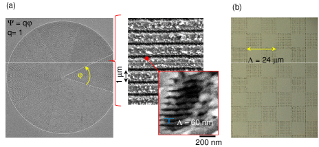
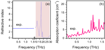
Figure 1(a) shows a pattern of grooves comprising an inhomogeneous birefringent plate with a topological defect of charge (hence -plate) for the azimuthal patterning of the optical axis. The azimuthal dependence of the slow axis is given by , where, is the half integer and is the polar angle. The laser ablated regions have nanoscale pattern of ripples with period scaling with wavelength and the refractive index, , as on dielectric (transparent materials) surfaces. Hence, by choosing wavelength different nano-structures can be formed. At tight focusing below the surface, voids can be created inside dielectric host material when a single pulse irradiance is TW/cm2 (Fig. 1(b)). Such surface and bulk modifications can be patterned with high precision and their use for tailoring optical, mechanical, and thermal properties are of interest. Optical characterisation of such patterns at T-ray region was carried out. Sapphire can be used as a substrate for optical elements due to its high transparency (Fig. 2) and performance of laser inscribed optical elements in T-ray region has to be well understood.
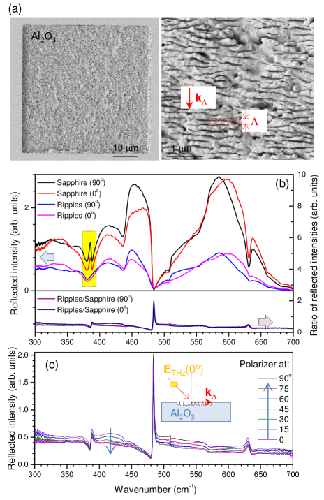
The TO phonon modes in -Al2O3 are at 385-388 cm-1 (TO1), 439 cm-1 (TO2) and 483 cm-1 (LO2) branches, 569 cm-1 (TO3) and 630 cm-1 (LO3), 633 cm-1 (TO4) and 1021 cm-1 (LO4) book ; all the values were taken from Table 5.2 of Ref. book . However, the best numerical fit of experimental sapphire’s reflectivity was achieved for LO4 at 906 cm-1 (not shown here). Figure 3(a) shows a strong alteration of reflectivity from laser ablated pattern of ripples at the TO1 mode at two different polariser orientations. Self-organised ripple structures with period of nm (Fig. 3(a)) or were recorded at the used laser wavelength nm and refractive index of sapphire . Strong relative reflectivity increase at the position of LO2 can be partially caused by a very low value of for the c-plane sapphire sample (a small values of denominator used in normalisation). There is an observable change in at the spectral location of TO4 mode. Reflection from the laser ablated surface shows spectrally broader TO1,4 bands (Fig. 3(a)), a sign of mode softening. Reflectivity interrogated at different linear polariser angles showed a consistent change in values of the TO1,4 bands.
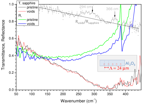
Figure 4 shows transmission and reflection spectra from the pattern of laser inscribed lines with period m. In the reflected spectrum a broad band around cm-1 was observed (or m in free space with refractive index ). The reflected wavelength is also the same which is effectively absorbed, hence, coupled into the structure/sample. The momentum conservation for the wavevectors of reflected light , structure/sample mode (could be a surface wave, SPP, TO-mode), and a grating is given by . This is the simplest two wave mixing scenario mediated by a grating. One can find the corresponding wavelength from the definition , at which the energy is deposited (absorbed) from the right triangle rule:
| (2) |
Equation 2 allows to calculate the wavelength and energy of the mode which is efficiently absorbing an incoming IR light and, hence, effectively reflecting it. One would find m (323 cm-1) with in sapphire for the high transmission region (Fig. 2). This did not fit the TO1 mode. The second reflectivity peak at 366 cm-1 (or m in free space) corresponds to the m or 390 cm-1 (Eqn. 2), which match the TO1 book . Since a square lattice was inscribed in sapphire (Fig. 2(c)), there is a mode with period . For this period the reflection peak at 366 cm-1 would correspond to m or 378 cm-1, which is also close to the TO1. For the opaque region (shaded in Fig. 1(a)), for the TO1,2 region and the same analysis using Eqn. 2 suggest the 366 cm-1 peak being close to the TO1 mode; similarly, the broad 294 cm-1 feature has no match with phonon mode. The broad 294 cm-1 reflection band can be due to a coupling with acoustic of hybrid modes Ishitani and would require a systematic study for different values matching the phonon modes.
Even though the reflectivity changes are very weak in the normalised spectrum (Fig. 4), they are discernable on a Rayleigh scattering slope (approximated by a line in this narrow spectral window). This proves that a designed periodic pattern can be used to couple energy into specific phonon mode.
IV Conclusions and outlook
It is demonstrated that surface and volume structuring of sapphire has direct impact on softening of TO phonon modes and changing reflectivity at a specific mode. Laser induced damage and structural disorder is the reason of this modification of phonon spectrum. Control of phonon spectrum is strongly required for the growth of layered structures where different optical and acoustic modes are coupling with the interface waves Ishitani . Among other possible applications are surface micro-texturing for ELO solutions in GaN-based LEDs, an electron mobility control in structures with strong phonon scattering, and in thermo-electrical materials for enhancement of difference between electron and phonon mean free path. Also a fast growing field of applications is in the design of flat optical elements using surface patterning Nivas where fs-laser surface and bulk structuring has been well developed 03apl2901 ; 02ass705p ; 16l .
This study was carried out as a part of the Australian synchrotron beamtime proposal M8468-2014. Partial support via Research Council Discovery grant DP130101205 and collaboration project with Workshop of Photonics, Ltd. is highly appreciated. Polished sapphire samples were donated by Tecdia Ltd. Financial support from the Research Council of Lithuania under the KITKAS project, contract No.LAT-04/2016. We acknowledge Teravil-Ekspla for the access to a commercial T-Spec THz-TDS system.
References
- (1) G. Mlnonl and G. Zerbl, “End effects on longitudinal accordion modes: Fatty acids and layered systems,” J. Phys. Chem. 86(24), pp. 4791 – 4798, 1982.
- (2) G. M. Png, R. J. Falconer, and D. Abbott, “Tracking aggregation and fibrillation of globular proteins using terahertz and far-infrared spectroscopies,” IEEE Trans. Terahertz Ssci. Technol. 6(1), pp. 45 –, 2016.
- (3) J. Doucet, I. Denicolo, and A. Craievich, “X- ray study of the rotator phase of the odd numbered paraffins C17H36, C19H40, and C21H44,” J. Chem. Phys. 75, pp. 1523 –, 1981.
- (4) J. D. Barnes and B. M. Fanconi, “Raman spectroscopy, rotational isomerism, and the “rotator” phase transition in n - alkanes,” J. Chem. Phys. 56, pp. 5190 – 5192, 1972.
- (5) A. I. Chumakov, G. Monaco, A. Monaco, W. A. Crichton, A. Bosak, R. Rüffer, A. Meyer, F. Kargl, L. Comez, D. Fioretto, H. Giefers, S. Roitsch, G. Wortmann, M. H. Manghnani, A. Hushur, Q. Williams, V. J. Balogh, V. K. Parlinski, P. Jochym, and P. Piekarz, “Equivalence of the boson peak in glasses to the transverse acoustic van Hove singularity in crystals,” Phys. Rev. Lett. 106, p. 225501, 2011.
- (6) X. Liu and K.-Q. Zhang, Silk Fiber - Molecular Formation Mechanism, Structure- Property Relationship and Advanced Applications. Intech, 2014.
- (7) S. Kim, B. Marelli, M. A. Brenckle, A. N. Mitropoulos, E.-S. Gil, K. Tsioris, H. Tao, D. L. Kaplan, and F. G. Omenetto, “All-water-based electron-beam lithography using silk as a resist,” Nat. Nanotechnol. 9, p. 306, 2014.
- (8) A. Balčytis, M. Ryu, G. Seniutinas, J. Juodkazytė, B. C. C. Cowie, P. R. Stoddart, J. Morikawa, and S. Juodkazis, “Black-CuO: Surface-enhanced Raman scattering and infrared properties,” Nanoscale 7(43), pp. 18299–18304, 2015.
- (9) Y.-L. Sun, Q. Li, S.-M. Sun, J.-C. Huang, B.-Y. Zheng, Q.-D. Chen, Z.-Z. Shao, and H.-B. Sun, “Aqueous multiphoton lithography with multifunctional silk-centred bio-resists,” Nature Commun. 6, p. 8612, 2015.
- (10) Y. Hu, Q. Zhang, R. You, L. Wang, and M. Li, “The relationship between secondary structure and biodegradation behavior of silk fibroin scaffolds,” Adv. Mat. Sci. Engineer. 2012, pp. 185905/1–5, 2012.
- (11) J. Morikawa, M. Ryu, A. Balčytis, G. Seniutinas, L. Fan, V. Mizeikis, J. L. Li, X. W. Wang, M. Zamengo, X. Wang, and S. Juodkazis, “Silk fibroin as water-soluble bio-resist and its thermal properties,” RSC Advances 6, pp. 11863 – 11869, 2015.
- (12) J.-J. Greffet, R. Carminati, K. Joulain, J.-P. Mulet, S. Mainguy, and Y. Chen, “Coherent emission of light by thermal sources,” Nature 416, pp. 61 – 64, 2002.
- (13) E. Jelmakas, A. Kadys, T. Malinauskas, D. Paipulas, D. Dobrovolskas, M. Dmukauskas, A. Selskis, S. Juodkazis, and R. Tomašiūnas, “A systematic study of light extraction efficiency enhancement depended on sapphire flipside surface patterning by femtosecond laser,” J. Physics D: Appli. Phys. 48(28), p. 285104, 2015.
- (14) Y. Ishitani, “Theoretical and experimental study of the optical absorption at longitudinal phonon or phonon-plasmon coupling mode energy: An example of GaN,” J. Appl. Phys. 112, p. 063531, 2012.
- (15) A. Sapphire: Material, Manufacturing, Springer Science + Business Media, New York, 2009.
- (16) O. Efimov, S. Juodkazis, and H. Misawa, “Intrinsic single and multiple pulse laser-induced damage in silicate glasses in the femtosecond-to-nanosecond region,” Phys. Rev. A 69, p. 042903, 2004.
- (17) M. Schubert, Infrared Ellipsometry on Semiconductor Layer Structures: Phonons, Plasmons, and Polaritons, Springer, Berlin.
- (18) J. JJ Nivas, S. He, A. Rubano, A. Vecchione, D. Paparo, L. Marrucci, R. Bruzzese, and S. Amoruso, “Direct femtosecond laser surface structuring with optical vortex beams generated by a q-plate,” Sci. Reports 5, p. 17929, 2015.
- (19) E. Vanagas, I. Kudryashov, D. Tuzhilin, S. Juodkazis, S. Matsuo, and H. Misawa, “Surface nanostructuring of borosilicate glass by femtosecond nJ energy pulses,” Appl. Phys. Lett. 82(17), pp. 2901–2903, 2003.
- (20) S. Juodkazis, S. Matsuo, H. Misawa, V. Mizeikis, A. Marcinkevicius, H. B. Sun, Y. Tokuda, M. Takahashi, T. Yoko, and J. Nishii, “Application of femtosecond laser pulses for microfabrication of transparent media,” Appl. Surf. Sci. 197-198, pp. 705–709, 2002.
- (21) M. Malinauskas, A. Žukauskas, S. Hasegawa, Y. Hayasaki, V. Mizeikis, R. Buividas, and S. Juodkazis, “Ultrafast laser processing of materials: from science to industry,” Light: Sci. Appl. , p. doi:10.1038/lsa.2016.133, 2016 (online 14 March).