Saving Moore’s Law Down To 1nm Channels With Anisotropic Effective Mass
Abstract
Scaling transistors’ dimensions has been the thrust for the semiconductor industry in the last 4 decades. However, scaling channel lengths beyond 10 nm has become exceptionally challenging due to the direct tunneling between source and drain which degrades gate control, switching functionality, and worsens power dissipation. Fortunately, the emergence of novel classes of materials with exotic properties in recent times has opened up new avenues in device design. Here, we show that by using channel materials with an anisotropic effective mass, the channel can be scaled down to 1nm and still provide an excellent switching performance in both MOSFETs and TFETs. In the case of TFETs, a novel design has been proposed to take advantage of anisotropic mass in both ON- and OFF-state of the TFETs. Full-band atomistic quantum transport simulations of phosphorene nanoribbon MOSFETs and TFETs based on the new design have been performed as a proof.
Shrinking the size of metal oxide semiconductor field effect transistors (MOSFETs) has improved the functionality, speed, and cost of microprocessors over the last four decades. However, the advantages of scaling are quickly fading away [1]. For example, the operational frequency of CPUs has stopped improving since 2003 due to power consumption of CPUs reaching their cooling limit (100W/cm2) [2]. Moreover, scaling down towards the few nanometer regime is becoming more challenging due to source-to-drain (SD) leakage current [19, 3]; the gate controlled potential barrier becomes more transparent as channel becomes shorter and direct SD tunneling increases. Another challenge in miniaturizing MOSFETs is scaling down the supply voltage [2]. A smaller can be achieved in a switch with sharper ON to OFF transition. However, the steepness of conventional MOSFETs have a fundamental limit due to thermionic injection of carriers over the channel barrier (60 at room temperature). Accordingly, in MOSFETs does not scale very well. On the other hand, tunnel FETs (TFETs) can, in principle, provide steeper switching [4, 5]. Nevertheless, scaling TFETs is even trickier than MOSFETs, since scaling affects both ON- and OFF-states of the TFETs [13, 6, 16]. Hence, the tremendous improvement in processing power of transistors every few years linked to the dimension scaling and empirically described by Moore’s law has reached a dead end. Fortunately, it is shown here that 2D materials with anisotropic effective mass () can be used to solve these problems and save Moore’s law.
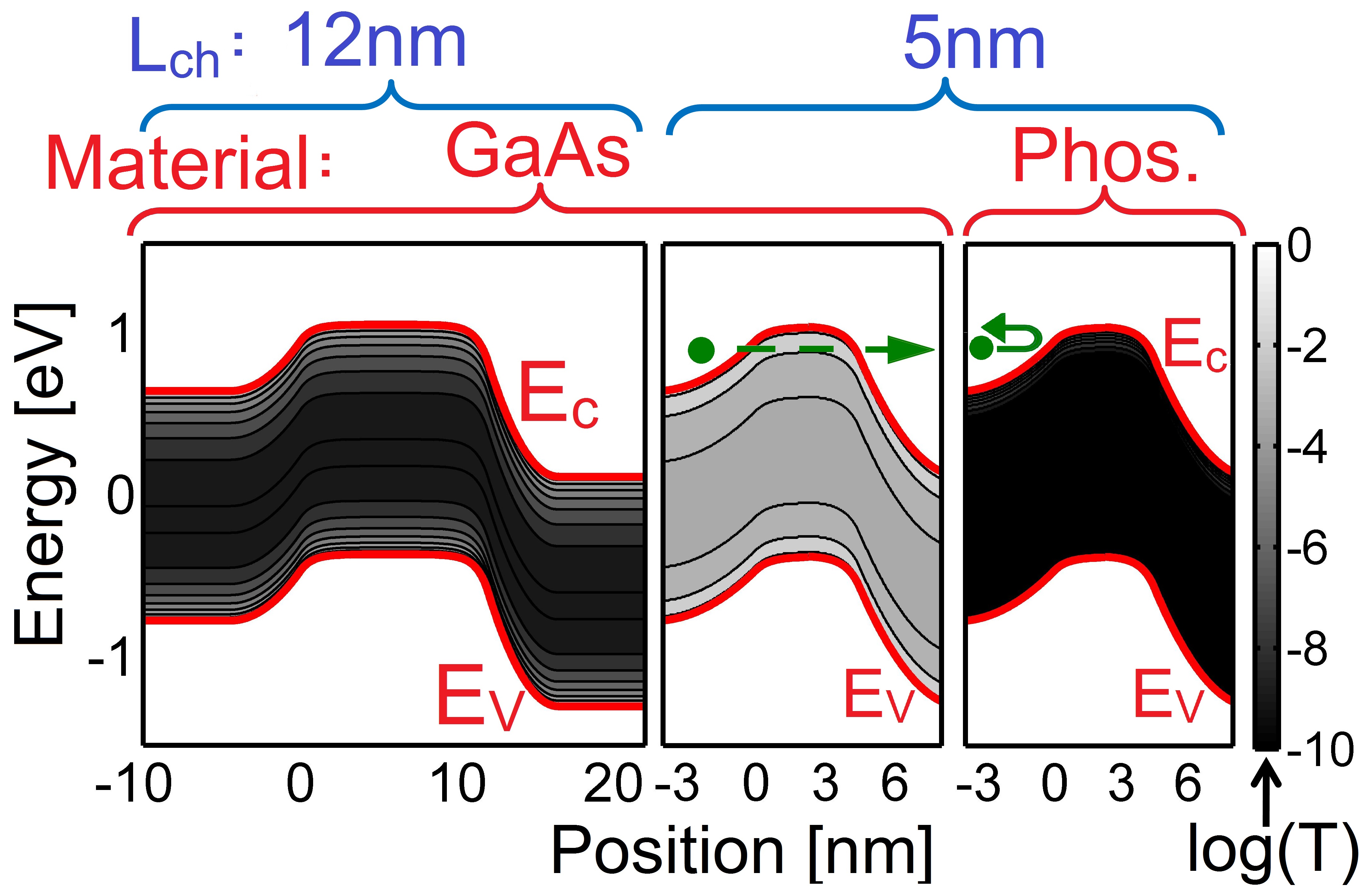
First, we discuss the source-to-drain tunneling challenge of the ultra scaled MOSFETs. Reducing the channel size makes the potential barrier more transparent. To visualize this, the transmission is shown in colormap on a logarithm scale and with an overlayed band diagram of MOSFETs in Fig. 1. The band diagram and transmission profile of a 12nm and 5nm long channel GaAs MOSFET are compared respectively in Fig. 1a and 1b. 5nm long channel GaAs MOSFET suffers significantly from SD leakage which reduces the gate control. Equation (1) shows the dependence of tunneling current through barrier on of the channel material. According to Equ. (1), an apparent solution to the high transparency of channel barriers in short channel regime is a channel material with higher effective mass.
| (1) |
Although high channel materials block SD tunneling effectively, they have a set of drawbacks too. Quantum capacitance () of channel material increases as a result of larger density of states (DOS) and . Accordingly, the gate capacitance () which is the net series capacitance of and oxide capacitance () increases. Hence, a larger translates into a larger switching delay ().
| (2) |
Anisotropic effective mass can provide a solution to this problem with reducing by a factor of . This reduction of is the result of the decreased density of states () in anisotropic materials:
| (3) |
where and are low and high effective masses of the channel material along its two main axes. If high axis of channel is aligned with transport direction and low axis is aligned with the confinement direction, both low transparency and small switching delay can be achieved. Note that high along the channel increases the carriers decay rate through barrier exponentially, whereas low confinement reduces DOS and . Hence, a 2D material such as phosphorene [9] with anisotropic [10] can provide an excellent switching performance in MOSFETs ensuring the continuation of Moore’s Law to atomic dimensions.
Here, we discuss the scaling challenge of TFETs. Although TFETs were intended to reduce the power consumption of transistors [4, 5], scaling TFETs below 10nm is even more challenging than MOSFETs [6, 16, 13]. The ON-state and OFF-state tunneling currents (ION and IOFF) depend on the same device parameters [24]. Thus decreasing IOFF would reduce ION. Roughly, the ON/OFF ratio of TFETs depends on [13, 24, 25]:
| (4) |
where and are the tunneling distances in the ON- and OFF-state respectively. and ( and ) are the reduced effective mass and the bandgap of the channel material (source-to-channel junction), respectively.
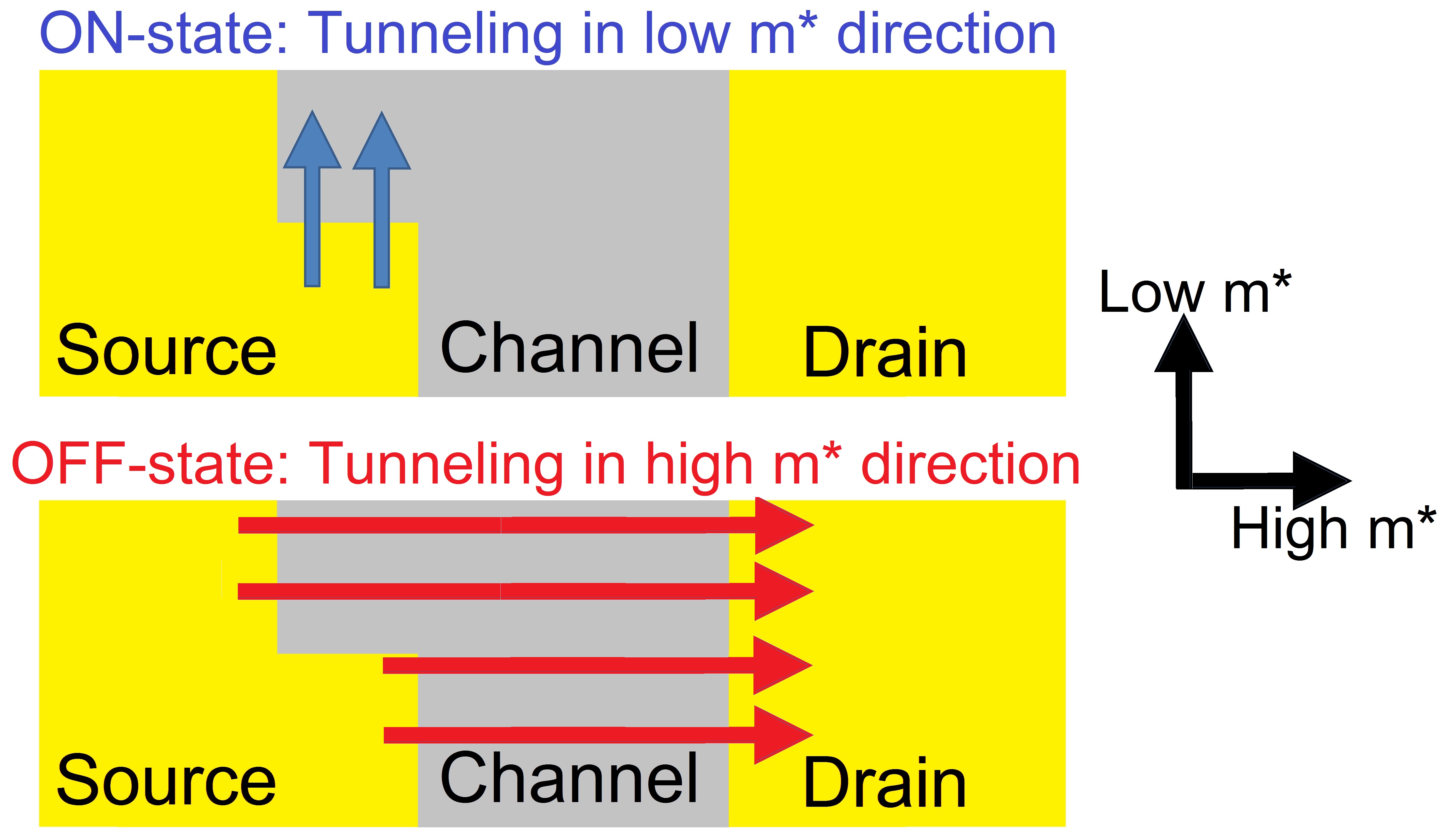
Shrinking the channel length to few nanometers brings close to 1 and reduces ION/IOFF significantly. One apparent solution can be a heterostructure channel where the term is much smaller than due to different materials used in the source and channel regions [18, 26]. However, heterostructure TFETs suffer from interface states which deteriorate their OFF-state performance [27, 28, 29]. Although homojunction TFETs do not have the interface states, it is challenging to provide high ON/OFF ratio especially below 6nm [13, 14]. Anisotropic effective mass can also provide a solution for this challenge by setting source-channel junction along low axis of channel material and the channel barrier along high axis.
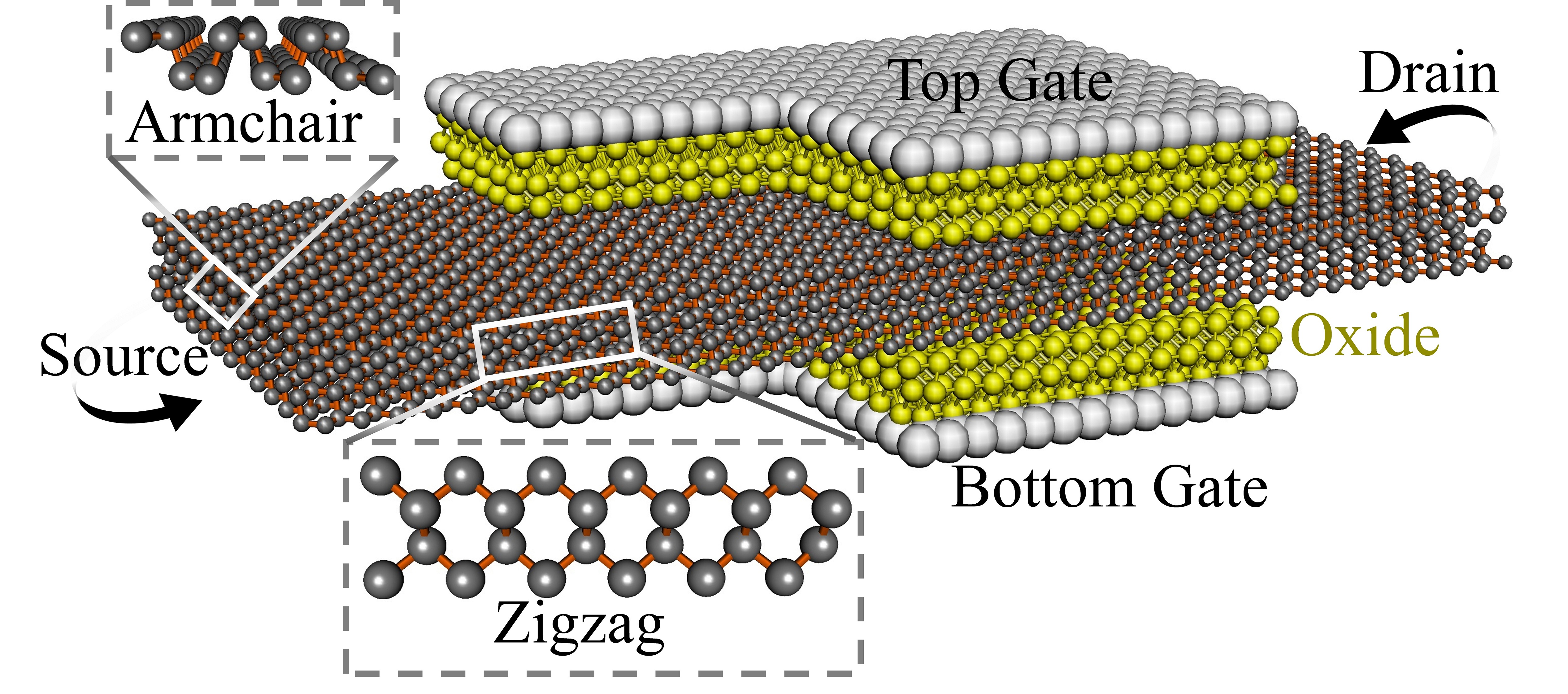
Although, many novel materials and designs have been proposed to enhance the performance of TFETs such as 2D material TFETs [7, 8, 15], Nitride heterostructures [18], dielectric engineering [17], there are not many proposals for solving the scaling challenge of TFETs [13]. In this work, a new TFET design is proposed to overcome the scaling challenge and enable downsizing to 2nm channel lengths. Fig. 2a shows a novel TFET device structure to take advantage of anisotropic effective mass. Notice that the gate is L-shaped. Fig. 2b depicts that the tunneling in the ON-state occurs along the low axis of the channel enhancing the ION. However, the tunneling in the OFF-state occurs along the high axis and results in a very low IOFF. Hence, this new TFET design can revive Moore’s law for sub-10nm TFETs.
In this work, phosphorene nanoribbon has been chosen as the channel material since it has a large effective mass anisotropy in zigzag and armchair directions. Moreover, multi-layer phosphorene provides a range of bandgap (1.45 to 0.4eV [11, 12]) suitable for transistor applications. of monolayer (1L-) and bilayer (2L-) phosphorene is about 1.45eV and 0.8eV, respectively. Since MOSFETs require larger for a smaller source-to-drain leakage, a monolayer phosphorene has been used here. The situation is more tricky in TFETs which need optimized . It was shown previously that 2L-phosphorene has an optimum , and hence 2L has been chosen for TFETs. HfO2 is used as the gate dielectric with an equivalent oxide thickness (EOT) of 0.5nm in both MOSFETs and TFETs and IOFF is set to .
Fig. 3a compares - of a conventional 2L-phosphorene nanoribbon along zigzag and armchair transport directions with L-shaped gate (L-gate) TFET calculated from full-band atomistic quantum transport simulations using NEMO5 [22, 23]. Not only does the L-gate TFET have ION close to that of the armchair ribbon (low ), but it also has IOFF similar to that of the zigzag ribbon (high ). Hence, the L-gate design has the advantages of both low and high devices simultaneously: high ION and low IOFF.
The performance of the L-gate TFET depends on the length (see Fig. 3b) which determines the width for ON-current. In conventional TFETs, equals 0. Fig. 3b shows ION of L-gate TFET as a function of for a fixed IOFF of 10. Increasing enhances ION significantly, however it reduces the source extension by . Accordingly, there is a limit on according to the footage requirements in the design. Nevertheless, a of about 2.5nm can improve the performance of TFET approximately by 2 orders of magnitude.
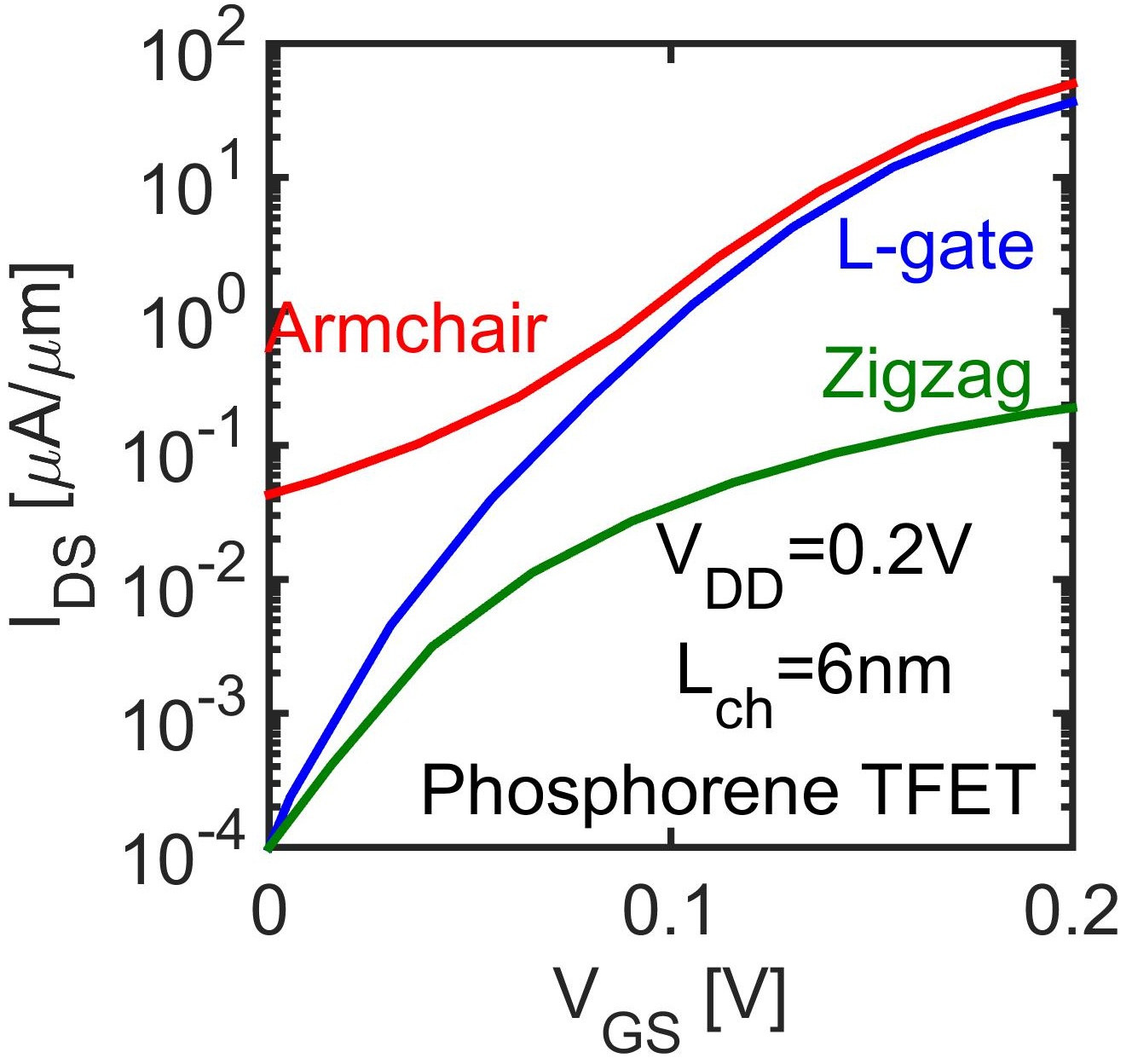
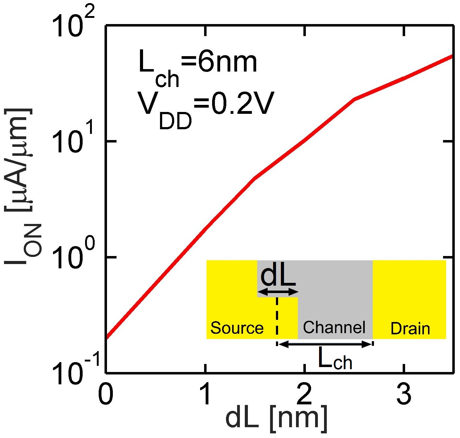
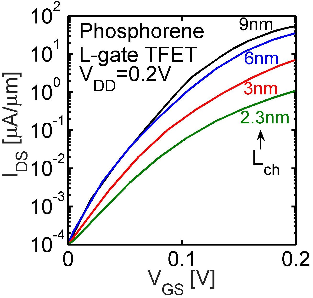
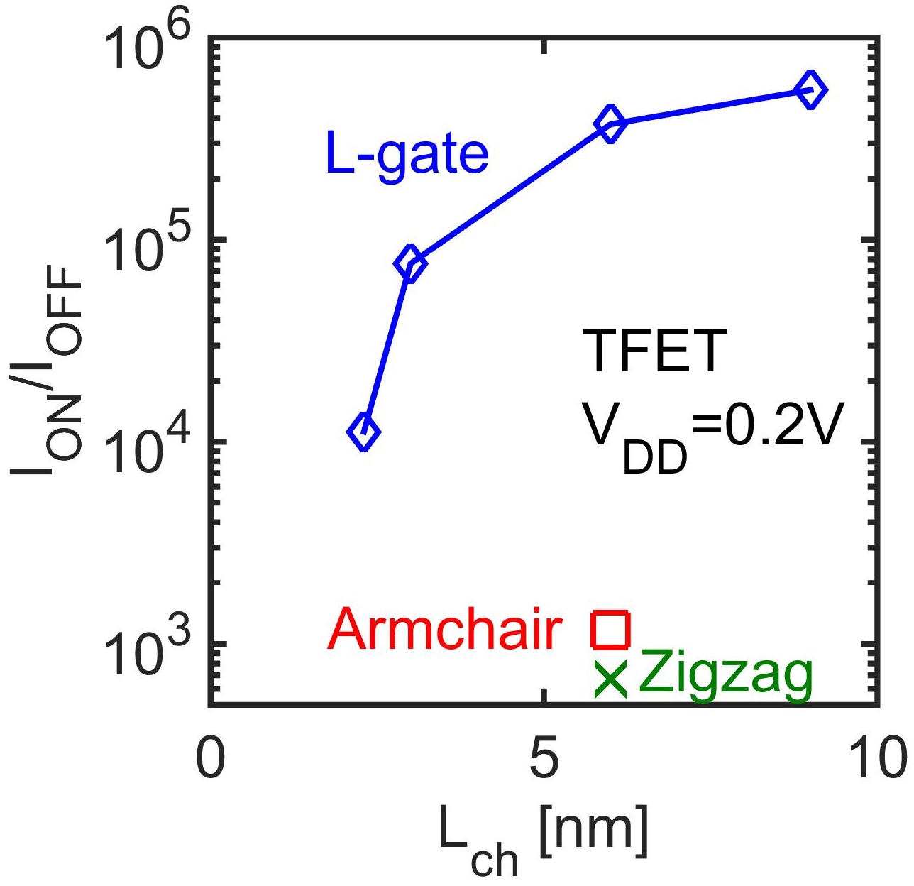
Fig. 3c shows ultra-scaled L-gate TFETs with channel lengths from 9nm down to 2.3nm with a of 0.2V. In ultra-scaled TFETs, cannot scale below since the maximum tunneling energy window is limited by . The L-gate TFETs with above 2nm provide ION/I and satisfy the minimal ITRS requirement for ION/IOFF ratio. Although the L-gate design has improved the performance of TFETs significantly, the ON-state performance of TFET decreases for devices with and below 2nm and 0.2V, respectively.
Fig. 3d shows ION/IOFF ratio of L-gate TFETs as a function of . Ultra-scaled channel lengths put a limit on . Hence, shrinks down from 3.5nm to 1nm when the channel length scales down from 9nm to 2.3nm. L-gate TFETs with channel lengths down to 2nm provide ION/IOFF ratio larger than 104 (required by ITRS as minimum amount of ION/IOFF ratio). This result proves that L-gate TFETs with a channel material of anisotropic enable successful scaling of TFETs down to the ultimate limit; a channel with a few atoms.
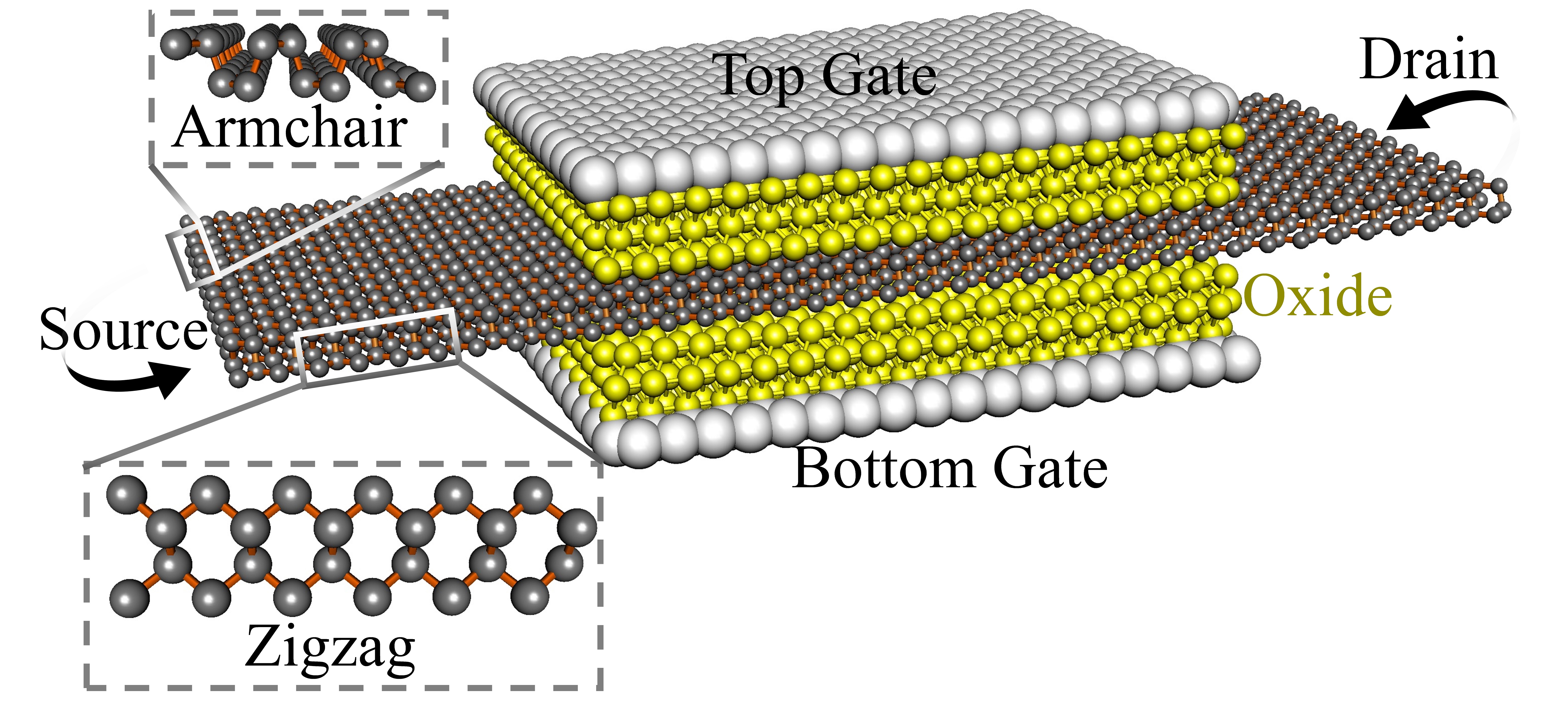
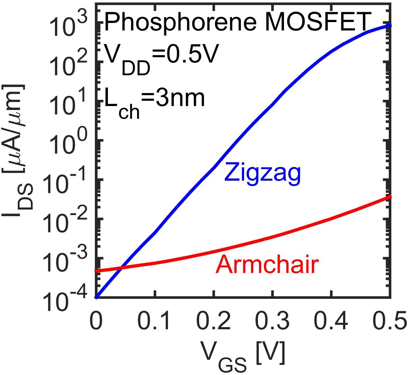
As mentioned before, ultra-scaled MOSFETs require large and to block source-to-drain tunneling. Hence, 1L-phosphorene nanoribbon has been chosen here which has the highest and compared to multilayer phosphorene. The schematic of the 1L-phosphorene MOSFET has been shown in Fig. 4a. The supply voltage is fixed to 0.5V, much higher than of TFETs, since the Boltzmann limit of subthreshold swing in MOSFETs (i.e. 60 mV/decade in room temperature) does not allow the scaling of .
The transfer characteristics of a short channel 1L-phosphorene (=3nm) with transport direction along low (armchair) and high (zigzag) are compared in Fig. 4b. As expected, the gate efficiency of a phosphorene MOSFET is much better when the high (zigzag) axis is along the transport direction. This better gate efficiency improves the subthreshold slope of MOSFET significantly.
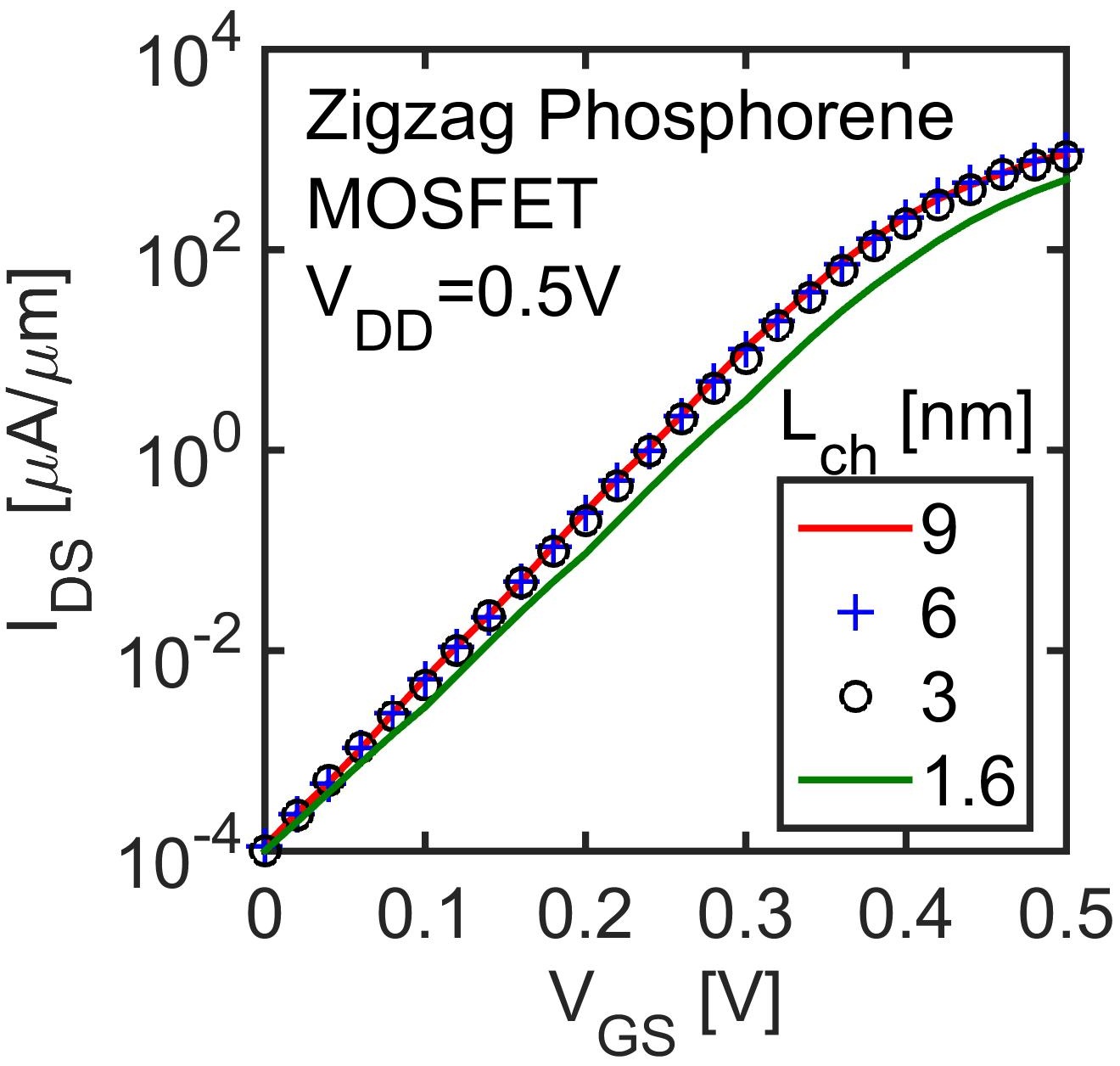
Fig. 4c shows - of zigzag scaled phosphorene MOSFETs with channel lengths from 12nm to 1.6nm. Notice that for phosphorene MOSFETs with an larger than and an ION/IOFF ratio larger than have been achieved. 1L-phosphorene MOSFETs show a significant advantage over other 2D materials whose performances are diminished below 5nm channel lengths [30].
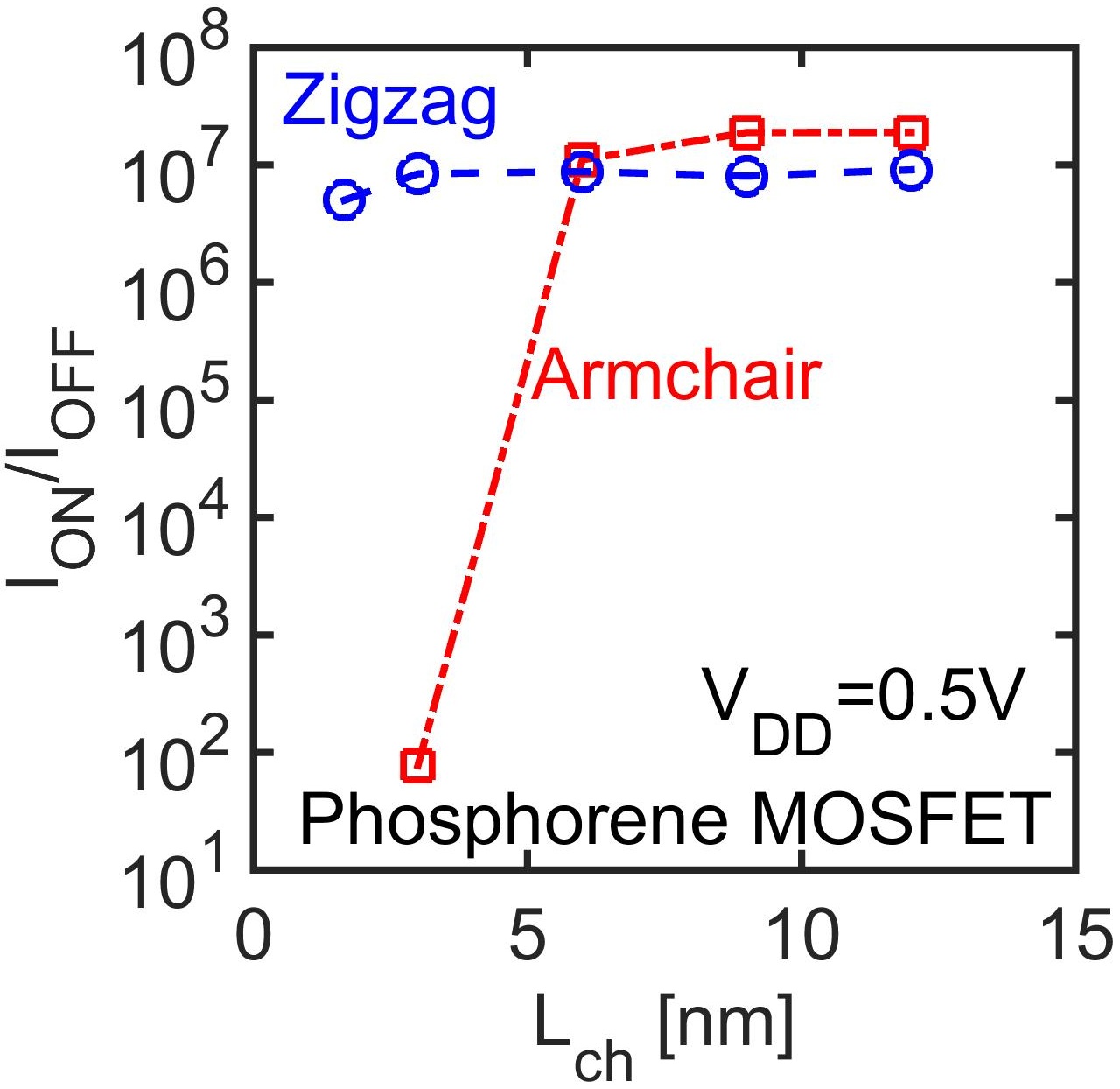
MOSFETs with long channels do not suffer from source-to-drain tunneling. Accordingly, a high transport is not required for blocking this leakage current. Actually, in long channel regime, a low transport can be beneficial and enhance the ON-state performance of the transistor since it leads to a higher carrier injection velocity. Fig. 4d shows ION/IOFF ratio of phosphorene nanoribbon MOSFETs as a function of along zigzag and armchair transport directions. Although zigzag nanoribbon MOSFETs significantly outperform the armchair ones in short channels due to lower source-to-drain tunneling, armchair nanoribbon MOSFETs show a better performance in longer channels due to higher injection velocity. There is a critical channel length (i.e. 6nm in 1L-phosphorene) in MOSFETs below which having a low becomes critical and above which a high is beneficial.
In summary, the channel materials with anisotropic effective mass can be used to design transistors scalable to 1-2nm channel lengths. In MOSFETs, the high effective mass along transport direction blocks the direct source to drain tunneling and low effective mass reduces the quantum capacitance and switching delay. On the other hand in TFETs, a novel L-shaped gate design is proposed which can provide advantage of high tunneling rate in the ON-state and low tunneling rate in OFF-state by engineering the tunneling paths along low and high effective mass directions. In summary, anisotropic effective mass can be used in an L-gate design to obtain large ON/OFF ratio in an ultra-scaled homojunction TFET.
Methods
The atomistic quantum transport simulation results have been obtained from the self consistent solution of 3D-Poisson equation and Non-equilibrium Green’s Functions (NEGF) method using the Nanoelectronics modeling tool NEMO5 [22, 23]. The Poisson equation provides the potential for NEGF method and takes the free charge in return. The tight-binding Hamiltonian of phosphorene used in NEGF calculations employs a 10 bands model. Phosphorene is a material with anisotropic dielectric properties. The details of the Poisson equation with anisotropic dielectric tensor and NEGF equations can be found in our previous works [7, 14].
Acknowledgment
This work was supported in part by the Center for Low Energy Systems Technology (LEAST), one of six centers of STARnet, a Semiconductor Research Corporation program sponsored by MARCO and DARPA.
References
- [1] A. M. Ionescu, and H. Riel, ”Tunnel field-effect transistors as energy-efficient electronic switches,” Nature, vol. 479, pp. 329–337 (2011).
- [2] K. Bernstein, R. K. Cavin, W. Porod, A. C. Seabaugh, and J. Welser ”Device and architectures outlook for beyond CMOS switches,” Proc. IEEE 98, 2169–2184 (2010).
- [3] J. Wang, and M. Lundstrom. ”Does source-to-drain tunneling limit the ultimate scaling of MOSFETs?” IEEE, International Electron Devices Meeting, IEDM (2002).
- [4] J. Appenzeller, Y.-M. Lin, J. Knoch, and Ph. Avouris, ”Band-to-band tunneling in carbon nanotube field-effect transistors,” Phys. Rev. Lett., vol. 93, no. 19, pp. 196805 (2004).
- [5] J. Appenzeller, Y.-M. Lin, J. Knoch, Z. Chen, and Ph. Avouris, ”Comparing carbon nanotube transistors-the ideal choice: a novel tunneling device design,” IEEE Trans. on Electron Dev. 52, 2568-2576 (2005).
- [6] U. E. Avci, and I. Young, ”Heterojunction TFET scaling and resonant-TFET for steep subthreshold slope at sub-9nm gate-length,” In IEEE International Electron Devices Meeting (IEDM), pp. 4-3. (2013).
- [7] H. Ilatikhameneh, Y. Tan, B. Novakovic, G. Klimeck, R. Rahman, J. Appenzeller, ”Tunnel Field-Effect Transistors in 2D Transition Metal Dichalcogenide Materials,” IEEE Exploratory Solid-State Computational Devices and Circuits, vol. 1, no. 1, pp. 12-18 (2015).
- [8] G. Fiori, F. Bonaccorso, G. Iannaccone, T. Palacios, D. Neumaier, A. Seabaugh, S. K. Banerjee, and L. Colombo, ”Electronics based on two-dimensional materials,” Nature nanotechnology, vol. 9, no. 10, pp. 768-779 (2014).
- [9] H. Liu, A. T. Neal, Z. Zhu, Z. Luo, X. Xu, D. Tom´anek, and P. D. Ye, ”Phosphorene: an unexplored 2d semiconductor with a high hole mobility,” ACS nano, vol. 8, no. 4, pp. 4033–4041, (2014).
- [10] J. Qiao, X. Kong, Z. X. Hu, F. Yang, and W. Ji, ”High-mobility transport anisotropy and linear dichroism in few-layer black phosphorus,” Nature communications, 5 (2014).
- [11] Y. Cai, G. Zhang, and Y. W. Zhang, ”Layer-dependent band alignment and work function of few-layer phosphorene,” Scientific reports, 4 (2014).
- [12] S. Das, W. Zhang, M. Demarteau, A. Hoffmann, M. Dubey, and A. Roelofs, ”Tunable transport gap in phosphorene,” Nano letters, 14(10), 5733-5739 (2014).
- [13] H. Ilatikhameneh, G. Klimeck, and R. Rahman ”Can Homojunction Tunnel FETs Scale Below 10nm?” IEEE EDL, vol. 37, no. 1, pp. 115-118 (2016).
- [14] T. A. Ameen, H. Ilatikhameneh, G. Klimeck, and R. Rahman ”Few-layer Phosphorene: An Ideal 2D Material For Tunnel Transistors,” [Online.] arXiv:1512.05021 (2015).
- [15] F. W. Chen, H. Ilatikhameneh, G. Klimeck, Z. Chen, and R. Rahman, ”Configurable Electrostatically Doped High Performance Bilayer Graphene Tunnel FET,” IEEE Journal of the Electron Devices Society (2016).
- [16] H. Lu, and A. Seabaugh, ”Tunnel Field-Effect transistors: state-of-the-art,” IEEE Electron Devices Society, vol. 2, no. 4, pp. 44-49 (2014).
- [17] H. Ilatikhameneh, T. Ameen, G. Klimeck, J. Appenzeller, and R. Rahman, ”Dielectric Engineered Tunnel Field-Effect Transistor,” IEEE Electron Device Letters (2015), 10.1109/LED.2015.2474147.
- [18] W. Li, S. Sharmin, H. Ilatikhameneh, R. Rahman, Y. Lu, J. Wang, X. Yan, A. Seabaugh, G. Klimeck, D. Jena, P. Fay, ”Polarization-Engineered III-Nitride Heterojunction Tunnel Field-Effect Transistors,” IEEE Exploratory Solid-State Computational Devices and Circuits, vol. 1, no. 1, pp. 28-34 (2015), DOI:10.1109/JXCDC.2015.2426433.
- [19] M. Salmani-Jelodar, S. Mehrotra, H. Ilatikhameneh, and G. Klimeck, ”Design Guidelines for Sub-12 nm Nanowire MOSFETs,” IEEE Trans. on Nanotechnology, vol. 14, no. 2, pp. 210-213 (2015).
- [20] R. B. Salazar, H. Ilatikhameneh, R. Rahman, G. Klimeck, J. Appenzeller, ”A predictive analytic model for high-performance tunneling field-effect transistors approaching non-equilibrium Green’s function simulations,” Journal of Applied Physics, 118, 164305 (2015), DOI:http://dx.doi.org/10.1063/1.4934682
- [21] M. Luisier, and G. Klimeck, ”Simulation of nanowire tunneling transistors: From the Wentzel–Kramers–Brillouin approximation to full-band phonon-assisted tunneling,” Journal of Applied Physics, vol. 107, no. 8, pp. 084507 (2010).
- [22] J. E. Fonseca, T. Kubis, M. Povolotskyi, B. Novakovic, A. Ajoy, G. Hegde, H. Ilatikhameneh, Z. Jiang, P. Sengupta, Y. Tan, G. Klimeck, ”Efficient and realistic device modeling from atomic detail to the nanoscale,” Journal of Computational Electronics, vol. 12, no. 4, pp. 592-600 (2013).
- [23] S. Steiger, M. Povolotskyi, H. H. Park, T. Kubis, and G. Klimeck, ”NEMO5: a parallel multiscale nanoelectronics modeling tool,” IEEE Transaction on Nanotechnology, vol. 10, no. 6, pp. 1464-1474 (2011).
- [24] H. Ilatikhameneh, R. B. Salazar, G. Klimeck, R. Rahman, J. Appenzeller, From Fowler-Nordheim to Non-Equilibrium Green’s Function Modeling of Tunneling, (2015) [Online.] http://arxiv.org/abs/1509.08170
- [25] E. O. Kane, ”Zener tunneling in semiconductors,” Journal of Physics and Chemistry of Solids, vol. 12, no. 2, pp. 181-188 (1960).
- [26] T. Krishnamohan, D. Kim, S. Raghunathan, and K. Saraswat. ”Double-Gate Strained-Ge Heterostructure Tunneling FET (TFET) With record high drive currents and subthreshold slope ¡¡ 60mV/dec,” In IEEE International Electron Devices Meeting IEDM, pp. 1-3 (2008).
- [27] J. Knoch, and J. Appenzeller. ”Modeling of high-performance p-type III–V heterojunction tunnel FETs,” IEEE Electron Device Letters, vol. 31, no. 4, pp. 305-307 (2010).
- [28] M. Kim, Y. K. Wakabayashi, M. Yokoyama, R. Nakane, M. Takenaka, and S. Takagi, ”Ge/Si Heterojunction Tunnel Field-Effect Transistors and Their Post Metallization Annealing Effect,” IEEE Transactions on Electron Devices, 62(1), 9-15 (2015).
- [29] S. Agarwal, and E. Yablonovitch, ”Band-Edge Steepness Obtained From Esaki/Backward Diode Current–Voltage Characteristics,” IEEE Transaction on Electron Devices, vol. 61, no. 5, pp. 1488-1493 (2014).
- [30] A.K.A Lu et al. ”Origin of the performances degradation of two-dimensional-based metal-oxide-semiconductor field effect transistors in the sub-10 nm regime: A first-principles study,” Applied Physics Letters 108.4, pp. 043504 (2016)
1 Author Contributions
H. I. came up with the idea of the L-gate TFET. H. I., T. A., and B. N. worked on the atomistic simulations and analyzed the data. Y. T. provided the tight binding model for phosphorene. G. K. and R.R. supervised the work. All authors contributed to writing the manuscript.
2 Competing financial interests
The authors declare no competing financial interests.