Influence of disordered edges on transport properties in graphene
Abstract
The influence of plasma etched sample edges on electrical transport and doping is studied. Through electrical transport measurements the overall doping and mobility are analyzed for mono- and bilayer graphene samples. As a result the edge contributes strongly to the overall doping of the samples. Furthermore the edge disorder can be found as the main limiting source of the mobility for narrow samples.
Since its discovery in 2004 graphene was praised as a new material with different possibilities in technical applicationsErscheinungspaper2004[1] ; Geimreport . It shows high mobility Mobility1 ; Mobility2 on silicon/silicon dioxide substrates on which it can be easily gated. Theoretical mobility limits were calculated Limitmob and confirmed in various experimental studiesOverview ; Geimreport . Transferring graphene on better and smoother substrates, e. g. Boron Nitride BN1 , or removing the substrate completely Suspended1 ; Suspended2 , lifted that limit and mobilities of over were measured Sus1Million . However these values only refer to non structured samples with undamaged edges. Edge disorder, introduced by various structuring techniques, can further limit the transport properties. Its negative impact is visible in mesoscopic transport measurements in graphene on silicondioxid SiO2Limits as well as on Boron NitrideBNlimits . Furthermore Raman spectroscopyRaman1 ; Raman2 ; raman2 and chemical doping studiesCarbonDoping hint towards the edge disorder not only as a mobility limit but a further doping source. Investigations of different kind of edge disorder were performed in previous studies on graphene nanoribbons (GNR) Z1 . It was shown that plasma etched or similar prepared GNR exhibit disordered sample etches and can lead to a reduction of conductance hinting to a further scattering mechanism Kats . Furthermore the influence of such disorder on electrical transport was studied on samples with varying widthW1 ; W3 ; W2 and an effect on transport properties was observed. Such disorder was also confirmed through Raman spectroscopy studies of GNRs edges raman1 . However a quantified evaluation of these edge effects were not presented, yet.
In this letter a quantified study is performed on mono- and bilayer samples. All flakes were structured in a similar Hall bar geometry with areas of different width. That specific shape allows to investigate the edge doping as well as the influence of edge disorder on the electrical transport in samples with equal bulk doping. Several graphene flakes were investigated within the scope of this study, showing similar results. In this letter, a monolayer and a bilayer sample are presented.
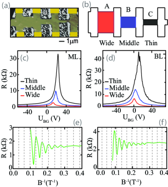
The sample preparation was done as following: Graphene flakes were placed on a silicon/ silicondioxide substrate. Afterwards the number of layers was analyzed using optical microscopy MakingGrapheneVisible . Plasma Oxygen Etching was used to edge the flakes into the geometrical shape, shown in Fig. 1(b). It is a Hall bar, which is divided into three different regions, named "wide", "middle", and "thin". Each part has the same length but differs in width. The length of each area is for the monolayer sample and for the bilayer, respectively. The Hall bar width is different for every area: (wide), (middle), and (thin) for the monolayer and , , and for the bilayer sample. Figure 1(a) shows an Atomic Force Microscope (AFM) image of a monolayer device. To reduce the overall doping the samples were mechanically cleaned by the AFM in contact modeAFMCleaning . Afterwards chromium/ gold contacts were evaporated. After the preparation process, the samples were loaded into a evaporation cryostat and measured at a base temperature of and a perpendicular magnetic field up to . The resistance was measured with a lock-in amplifier using an AC current of with a frequency of .
The characterization of the samples was conducted for each area using a four terminal set-up. Magnetotransport measurements were performed to confirm the number of layers. Figure 1(e) and (f) show the longitudinal resistance versus the inverse magnetic field. Shubnikov-de Haas oscillations are visible and the Berry phase can be extracted through extrapolation to zero. The Berry Phase is for the monolayer as expected and for the bilayer sample, which confirms the previous contrast analysis. Figure 1(c) and (d) show the resistance measurements versus the backgate voltage for different areas and samples. For each area a field effect is observed. However the position and the resistance of the charge neutrality point differs. In both cases the mono- and the bilayer sample follow the same trend. The thin part of both samples exhibits the highest resistance reaching for the monolayer sample and for the bilayer sample at the charge neutrality point. The resistance decreases with increasing width as expected for the geometry. In contrast, the dependence of the charge neutrality point position is not that simple. The overall doping of both samples is in the positive backgate voltage region, meaning that both samples are p-doped. However the doping concentration differs for every area. Because of the AFM cleaning the bulk of both samples can be ruled out as the origin of the doping change. However a disordered edge can act as a p-doping source, as was shown in previous works CarbonDoping . To analyze the amount of edge doping in these samples a simple approach is proposed. The overall doping amount of the sample , is the sum of the bulk doping and the edge doping ,
with being the doping concentration and the area, length, and width of the doped region. One can rewrite that approach to the doping concentration, leading to a width dependence:
From the backgate voltage at the charge neutrality point the overall doping can be calculated for all areas and both samples.
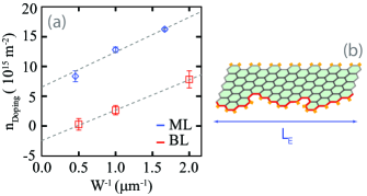
Figure 2(a) shows the overall doping concentration plotted versus the inverse Hall bar width. For both samples a linear dependence of the doping concentration is observed. Using the bulk-edge-doping approach shown above, the individual doping contributions components can be calculated for both samples. The bulk doping concentration is and for the mono- and bilayer, respectively. The edge doping concentration is for the monolayer and an almost equal concentration of for the bilayer sample leading to effective 2D-doping at the edge. To demonstrate the contribution of the doping components the actual doping amount is calculated for the thinnest area for the bilayer sample, where electrons and holes are introduced into the system through the bulk and the edge. One can clearly see the domination of the edge doping in this area. It is higher than the bulk contribution by a factor of , introducing holes as a main doping type. Such charge localization at sample edges was observed in ultra thin graphene nanoribbons Z1 . Furthermore it was found that additional edges in form of a cut or defects in the graphene bulk constitute a p-doping source and can be used to create p-n junctions AFMPN .
It is clear that the edge of the sample can be seen as a doping source. Furthermore we can assume that the adatoms causing the edge p-doping are oxygen compounds that adjusted itself on the graphene edge during the plasma oxygen structuring process, as is shown in a schematic in Fig. 2(b) (orange lines). To calculate the efficiency for edge doping, it is first assumed that a dangling bond can contribute to the overall doping by a count of doping carrier. However, assuming a zigzag edge, it is only possible once per , as is shown in Fig. 2(b). Taking into account that every side of the sample contributes to the edge doping an approximate efficiency of is calculated for the monolayer. As one can extract from the slopes in Fig. 2(a), the bilayer exhibits almost the same edge doping contribution and doping efficiency as the monolayer sample. Furthermore the doping efficiency of the plasma etched edges is comparable to an intentional chemical edge doping with hydrogen silsesquioxane, which was investigated in Ref. CarbonDoping, . The resulting efficiency is only slightly higher (0.85) than of the observed values in the presented study.
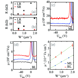
We further analyze the effect of the disordered plasma etched graphene edge on the electrical transport. The mobility was calculated from the measured resistance versus the backgate-voltage shown in Fig. 1(c) and (d). For this analysis the resistance was split up into two different parts: component caused by short range resistance and caused by long range resistance. Both components can be separated using the constant mobility Ansatz CMA . In contrast to the doping the short range resistance component stays almost constant throughout all sample areas: (wide), (mid), and (narrow) for the monolayer and (wide), (mid), (narrow) for the bilayer sample, respectively. Figure 3(a) and (b) shows the comparison between the short and the long range resistance component for a fixed charge carrier concentration for mono- and bilayer sample, respectively. As one can see the short range component undergoes a slight change of and is tiny compared to the change in the long range resistance, which is in the order of . Furthermore the difference of the short range component with changing width is quite small in comparison to the total short range resistance amount. The origin of the short range component can be located in the bulk and the edge of the sample. However the fact that the short range resistance stays almost constant while the width and with that the area changes indicates that the main short range scattering contributors are located at the edge of the investigated samples, which has the same length for all the samples.
Subsequently, the constant mobility is calculated from long range resistance component, i. e. the overall resistance after subtracting the short range component. The results are shown in Fig. 3(c) and (d). For both samples the mobilities differ with changing width. Additionally the monolayer exhibits a significantly higher mobility for every region as the bilayer, which is an expected behavior for increasing number of layers MobLayers . Interestingly, an overall dependence similar to the doping analysis can be observed: The highest mobility is obtained for the wide region (monolayer: , bilayer: ) and the lowest for the narrow region (monolayer: , bilayer: ). The middle section exhibits an intermediate mobility for mono- and for bilayer. Furthermore a significant difference between holes and electrons was not observed.
Hence it follows the same trend as the overall doping, the inverse mobility is plotted versus the inverse width, which is shown in Fig. 3(e). Equivalent to the overall doping concentration it is showing a linear increase with inverse width in the measurement range. The dependence of the mobility on the width is hinting towards an additional scattering mechanism at the sample edges. Since this correlation is detected in the mobility calculated from the long range resistance component, the origin of this mechanism is most likely caused by the additional edge dopingDAcc shown above.
By fitting the data in Fig. 3(e) linearly and extrapolating to an infinite sample width, the bulk mobility component can be estimated to for the bilayer and for the monolayer sample. Both bulk mobilities exceed the measured mobilities proving the limiting nature of the edge disorder. However it is important to notice, that these same results are an extrapolation of the observed mobilities and not measured.
As stated above, previous analysis were performed on the topic of edge disorder leading to an increasing resistance W1 ; W3 ; W2 . Our sample geometry allowed to investigate the edge disorder systematically excluding other effects. By extracting the electronic properties from the field effect for every different region we were able to analyze the short and the long range component independently. Our results show that the edge affects both, however, the long range far more than the short range resistance, subsequently influencing the overall mobility greatly. Therefore the edge doping can be seen as a strong scattering mechanism determining the electrical properties even in large, -sized samples.
In conclusion, we have reported an investigation of the influence of the edge disorder on the electrical transport in mono- and bilayer graphene. Our devices allowed to investigate the dependency of various properties on the width of each single sample. We showed how the edge influences the electrical transport greatly, dominates the overall doping, and acts as an additional scattering mechanism.
We acknowledge the financial support by the DFG via SPP 1459 and the Russian Foundation for Basic Research (Grant
No. 13-02-00326 a). We are grateful to A. P. Dmitriev, for helpful discussions. Authors D. S. and G. Yu. V. contributed equally to this work.
References
- (1) K. S. Novesolelov, A. K. Geim, S. V. Morozov, D. Jiang, Y. Zhang, S. V. Dubonos, I. V. Grigorieva, and A. A. Firsov, Science 306, 666 (2004).
- (2) A. K. Geim, Science 324, 1530 (2009).
- (3) S. V. Morozov, K. S. Novoselov, M. I. Katsnelson, F. Schedin, D. C. Elias, J. A. Jasczak, and A. K. Geim, Phys. Rev. Lett. 98, 186806 (2007).
- (4) E. H. Hwang, S. Adam, and S. Das Sarma, Phys. Rev. Lett. 100, 01660, (2008).
- (5) J. H. Chen, C. Jang, S. Xiao, M. Ishigami, and M. S. Fuhrer, Nature Nanotechnology 3, 206 (2008).
- (6) A. K. Geim and K. S. Novoselov, Nature Materials 6, 183 (2007).
- (7) C. R. Dean, A. F. Young, I. Meric, C. LeeL. Wang, S. Sorgenfrei, K. Watanabe, T. Taniguchi, P. Kim, K. L. Shepard, and J. Hone, Nature Nanotechnology 5, 722 (2010).
- (8) J. C. Meyer, A. K. Geim, M. I. Katsnelson, K. S. Novoselov, T. J. Booth, and S. Roth, Nature 446, 60 (2007).
- (9) X. Du, I. Skachko, A. Barker, and E. Y. Andrei, Nature Nanotechnology 3, 491 (2008).
- (10) E. V. Castro, H. Ochoa, M. I. Katsnelson, R. V. Gorbachev, D. C. Elias, K. S. Novoselov, A. K. Geim, and F. Guinea, Phys. Rev. Lett. 105, 266601 (2010).
- (11) D. Smirnov, J. C. Rode, and R. J. Haug, Appl. Phys. Lett. 105, 082112 (2014).
- (12) D. Bishoff, T. Krähenmann, S. Dröscher, M. A. Gruner, C. Barraudm, T. Ihn, and K. Ensslin, Appl. Phys. Lett. 101, 203103 (2012).
- (13) S. Heydrich, M. Hirmer, C. Preis, T. Korn, J. Eroms, D. Weiss, and C. Schüller, Appl. Phys. Lett. 97, 043113 (2010).
- (14) J. Dauber, B. Terrés, C. Volk, S. Trellenkamp, and C. Stampfer, Appl. Phys. Lett. 104, 083105 (2014).
- (15) C. Casiraghi, A. Hartschuh, H. Qian, S. Piscanec, C. Georgi, A. Fasoli, K. S. Novoselov, D. M. Basko, and A. C. Ferrari, Nano. Lett. 9, 1433-1441 (2009).
- (16) K. Brenner, Y. Yang, and R. Murali, Carbon 50, 637 (2012).
- (17) D. Bischoff, P. Simonet, A. Varlet, H. C. Overweg, M. Eich, T. Ihn, and K. Ensslin, Phys. Status Solidi RRL 1-7 (2015).
- (18) V. K. Dugaev and M. I. Katsnelson, Phys. Rev. B 88, 235432 (2013).
- (19) Y. Yang and R. Murali, IEEE Electron device Lett., 31, 383 (2010).
- (20) G. Xu, C. M. Torres, Jr. J. Tanf, J, Bai, E. B. Song, Y. Huang, X. Duan,Y. Zhang, and K. L. Wang, Nano Lett., 11, 1082 (2011).
- (21) A. Venugopal, J. Chan, X. Li, C. W. Magnuson, W. P. Kirk, L. Colombo, Rodney, S. Ruoff, and E. M. Vogel, J. App. Phys., 109, 104511 (2011).
- (22) D. Bischoff, J. Güttinger, S. Dröscher, T Ihn, K. Ensslin, and C. Stampfer, J. Appl. Phys. 109, 073710 (2011).
- (23) P. Blake, E. W. Hill, A. H. Castro Neto, K. S. Novoselov, D. Jiang, R. Yang, T. J. Booth, and A. K.Geim, Appl. Phys. Lett. 91, 063124 (2007).
- (24) A. M. Goossens, V. E. Calado, A. Barreiro, K. Watanabe, T. Taniguchi, and L. M. K. Vandersypen, App. Phys. Lett., 100, 073110 (2012).
- (25) H. Schmidt, J. C. Rode, C. Belke, D. Smirnov, and R. J. Haug, Phys. Rev. B 88, 075418 (2013).
- (26) S. Kim, J. Nah, I. Jo, D. Shahrjerdi, L. Colombo, Z. Yao, E. Tutuc, And S. K. Banerjee, App. Phys. Lett., 94, 062107 (2009).
- (27) M. F. Cracuin, S. Russo, M. Yamamoto, J. B. Oostinga, A. F. Morpurgo, and S. Tarucha, Nature Nanotechnology 4, 383 (2009). Phys. Rev. B, 81, 155454 (2010).
- (28) P. G. Silvestrov and K. B. Efetov, Phys. Rev. B 77, 155436 (2008).