Electromagnetic properties of a double layer graphene system with electron-hole pairing
Abstract
We study electromagnetic properties of a double layer graphene system in which electrons from one layer are coupled with holes from the other layer. The gauge invariant linear response functions are obtained. The frequency dependences of the transmission, reflection and absorption coefficients are computed. We predict a peak in the reflection and absorption at the frequency equals to the gap in the quasiparticle spectrum. It is shown that the electron-hole pairing results in an essential modification of the spectrum of surface TM plasmons. We find that the optical TM mode splits into a low frequency undamped branch and a high frequency damped branch. At zero temperature the lower branch disappears. It is established that the pairing does not influence the acoustic TM mode. It is also shown that the pairing opens the frequency window in the subgap range for the surface TE wave.
pacs:
72.80.Vp; 73.20.Mf; 78.67.WjI Introduction
Electron-hole pairing in a system of two conducting layers with oppositely charged carriers was predicted in 1 ; 2 . Such a system below the Kosterlitz-Thouless transition temperature may support a superflow of electron-hole pairs. It should result in zero resistance under a flow of oppositely directed and equal in modulus electrical currents in the adjacent layers.
Zero counterflow resistance has not been observed yet, but a number of experiments confirm that the pairing occurs. The increase in the interlayer drag resistance at low temperatures was detected in a double quantum well in AlGaAs heterostructures 3 ; 4 and in hybrid double layer systems comprising a single-layer (bilayer) graphene in close proximity to a quantum well created in GaAs5 . The upturn of the drag resistivity witnesses for the approaching the paired state 6 ; 6a . The electron-hole pairing was also predicted7 ; 8 ; 9 for quantum Hall bilayers where the overall filling factor of the lowest Landau level of two layers is close to unity. The pairing was confirmed by transport experiments10 ; 11 ; 12 where an exponential increase of the longitudinal counterflow conductivity and the vanishing of Hall resistance were discovered. Recent observation of a perfect longitudinal interlayer drag in the Corbino disk geometry 14 also witnesses for the electron-hole pairing.
After the experimental discovery of graphene the double layer graphene systems are considered as perspective ones for achieving the electron-hole pairing and counterflow superconductivity 15 ; 16 ; 17 . Potentially, such systems have a number of advantages. In graphene the electron and hole spectra coincide with each other at low energies and the condition of nesting of the electron and hole Fermi surfaces is fulfilled automatically. There is no gap between the electron and hole subbands and the density of carriers in the electron and hole layers can be easily controlled by external gates. At last, conducting electrons in graphene do not undergo a localization at low density of carriers.
The main obstacle in realizing the electron-hole pairing in graphene is the screening of the Coulomb interaction between electrons and holes18 ; 18a . Strictly spearing, the same obstacle emerges for the carriers with the quadratic spectrum, but in the latter case relatively high temperature of pairing can be achieved in the low density limit. In this limit electrons and holes bind in small size pairs (smaller than the average distance between the pairs) and the screening is suppressed. The Dirac carriers are not coupled in small size pairs, but they may form large size electron-hole pairs analogous to the Cooper pairs. Then the screening is also suppressed. Depending on the material parameters two situations are possible. If the bare interaction is weak, the screening will be strong and the critical temperature will be very low. Such a case was analyzed in 18a . On the contrary, if the bare interaction is strong, the pairing will be accompanied by an essential weakening of screening and it will occur at high temperature 19 ; 20 . The latter possibility can be realized if the Coulomb interaction strength exceeds certain critical value and the distance between the graphene layers related to the inverse Fermi wave number is small: . The interaction strength (also called the effective fine structure constant) is defined as , where is the Fermi velocity and is the dielectric constant of the surrounding media. The parameter grows up under increase in the number of Dirac components (number of valleys times the number of spin components). For graphene () the dynamical screening theory19 yields . Thus a double layer graphene system in a vacuum ( and ) can be in a paired state at relatively high temperatures ( K). Other known two-dimensional Dirac crystals (silicene, germanene 21 ; 22 , -graphyneagr ) have the same number of Dirac components, but smaller . Having the parameter approximately in two times larger than one for graphene, double layer silicene, germanene and -graphyne look more promising for achieving high critical temperature. In particular, a double layer silicene(germanene) system embedded into a nanoporous or nanostructured matrix with np1 ; np can also demonstrate the electron-hole pairing at high temperature. Another perspective system is a topological insulator (TI)24 . Two opposite surfaces of a TI plate serve as two adjacent conducting layers. The spectrum of the surface states of TI has an odd number of Dirac cones. For the critical parameter 19 and the pairing at high temperature is possible in a TI plate embedded in a dielectric media with 25 . One can also mention a possibility pmf of reducing the Fermi velocity in graphene and shifting the system parameters into the strongly coupled pairing regime by a periodic magnetic field.
Electron-hole pairing was also predicted for double layer graphene systems subjected to a strong uniform magnetic field directed perpendicular to the layers b1 ; k1 ; f1 ; f2 . The important advantage of the quantum Hall state in Dirac spectrum systems is a large energy gap between the zeroth and the first Landau level. The screening in this case is considerable reduced even without pairing. Double layer system made of graphene sheets with the band gap (induced, for instance, by hydrogenation) is also a promising candidate for obtaining the electron-hole superfluidity ke . The presence of the gap makes the formation of small size local pairs possible. One can expect that in that case the screening will be of a minor importance.
A direct manifestation of the electron-hole pairing would be an observation of zero counterflow resistance. But since in two-dimensional superfluid systems a flow causes unbinding of vortex pairs, a small voltage appears in any case. The presence of areas where the pairing is suppressed (in the case of system composed of puddles of the superconductive phase26 ), can be another source of nonzero resistance. Therefore, it is desirable to have an independent indicator of pairing. For usual superconductors the Meissner effect can serve as such an indicator. Diamagnetic response of a double layer system with electron-hole pairing is very small1 ; 27 and it cannot be used for detection of the pairing. The pairing may reveals itself in a considerable enhancement of tunneling conductivity in the vicinity of the critical temperature ef-loz . This phenomenon interpreted as a fluctuational internal Josephson effect is the general one for electron-hole bilayers and it can be used as an indicator of pairing. The pairing reduces screening that can be seen by measuring the electric field of a test charge located near graphene layers. A strong increase of this field under lowering in temperature can be considered as a universal hallmark of the electron-hole pairing 27 , but it requires sensitive sensors with high spatial resolution.
In this paper we consider microwave methods of indirect observation of the pairing with reference to a double layer graphene system made of two gapless monolayer graphene sheets in zero magnetic field. We study the influence of the electron-hole pairing on the transmission and reflection characteristics of double layer graphene systems. We also analyze how the pairing changes the spectrum of surface plasmon-polaritons in double layer graphene systems. In Sec. II we develop the approach based on the generalized Nambu formalism. In difference with the original Nambu approach28 we use the matrix Green’s function of dimension . In Sec. III gauge invariant linear response functions are obtained. In Sec. IV an influence of the pairing on the transmission, reflection and absorption of electromagnetic waves in a double layer graphene system is analyzed. In Sec. V surface TM and TE waves in a double layer graphene system with the electron-hole pairing are studied.
II Extended Nambu formalism for a double layer graphene
In the low-energy approximation the conducting electrons in a graphene layer are described by the matrix Hamiltonian
| (1) |
where are the Pauli matrices, is the identity matrix, is the wave vector counted from the Dirac point, is the chemical potential, is the valley index, is the spin index, and are the electron creation and annihilation operators that have the spinor structure
| (2) |
The components of the pseudospinors (2) are the operators of creation and annihilation of electrons in the graphene sublattices A and B.
A double layer system with the electron-hole pairing is described by the mean-field Hamiltonian presented in terms of 4-component spinors 17
| (3) |
where
| (4) |
and and are the layer indexes. In the Hamiltonian (3) are the matrices defined through the direct product
| (5) |
We imply the electron density in the layer 1 equals the hole density in the layer 2. It corresponds to . Eq. (3) contains the order parameter of the electron-hole pairing and the Hartree-Fock potential . These quantities have to be found from the self-consistence equations.
In the general case mink the order parameter is a matrix , components of which describe the pairing of an electron in the sublattice and a hole in the sublattice . This matrix can be expressed through the Pauli matrices . In this paper we consider the state, where only is nonzero. It corresponds to the maximum energy gap in the quasiparticle spectrum and the minimum of the ground state energy17 .
We would note the difference between the formalism used here and the approach 15 ; 16 ; 19 ; 20 ; 27 in which the standard Nambu notation28 can be used27 . In the latter case the order parameter is defined as an average , where is the operator of electron creation in the state with the wave vector in the Dirac subband in the layer . The single layer Hamiltonian (1) written in terms of operators has the scalar form. Then the Hamiltonian of a double layer system can be written in terms of two-component spinors.
In the extended Nambu formalism the Green’s function is a matrix
| (6) |
Here and below we set . The Green’s function (6) has the valley and the spin indices. Each spin-valley component contributes additively to the response functions and these contributions do not depend on and . Therefore, one can consider only one component and take into account the other components by the factor in the final answer. Below we do the computations for component and omit the spin and valley indexes.
It is convenient to present the Green’s function (6) in the form
| (7) |
where
| (8) |
and . The matrices , are expressed through the matrices:
| (9) |
| (10) |
where is the angle between the wave vector and the axes.
The interaction part of the Hamiltonian written in terms of four-component spinors (4) reads
| (11) | |||
| (12) |
where is the area of the system, the notation means the normal ordering, , and , are the Fourier-components of the intralayer and interlayer Coulomb interaction, respectively. We specify the case of a uniform dielectric environment that corresponds to the same intralayer interaction potential in both layers. The second sum in Eq. (11) compensates the mean-field terms in the Hamiltonian (3).
The self-consistence condition requires the nullifying of the lowest order self-energy correction to the mean-field Green’s function (6). The self-energy is the matrix and the self-consistence equation has the matrix form equivalent to 16 scalar equations. Most of them are satisfied by symmetry. Nontrivial ones are the self-consistence equation for the Hartree-Fock potential and the equation for the order parameter . The main effect of the Hartree-Fock potential is an unessential shift of the chemical potential that can be included in the definition of . The order parameter satisfies the equation
| (13) |
where is the temperature. We note that Eq. (13) does not contain the factor with cosine in difference with the self-consistence equation used in 15 ; 16 ; 19 ; 20 ; 27 . The origin of this difference is that the order parameter introduced in the Hamiltonian (3) does not depend on . In the approach 15 ; 16 ; 19 ; 20 ; 27 the order parameter depends on . In that case the self-consistence equation has the form
| (14) |
The consistence of Eq. (14) with the condition requires zero contribution of the term with cosine into the integral in Eq. (14). Then Eq. (14) reduces to Eq. (13).
The screening can be taken into account by replacing the bare interaction with the screened one. In the random phase approximation the Fourier-component of the screened interaction reads
| (15) |
where are the density-density response functions defined below.
III Ward identity and gauge invariance of the response functions
The interaction of the double layer graphene system with the electromagnetic field is described by the Hamiltonian
| (17) |
where are the charge density operators, - are the current density operators (), - are the vector potentials, , are the scalar potentials, and is the light velocity. The index () notates the sum (difference) of the corresponding quantities in the layers 1 and 2. The charge and current density operators are given by the equation
| (18) |
where the vertexes have the matrix form
| (19) |
In the linear response approximation the currents are the linear functions of the potentials :
| (20) |
The response functions are obtained as the analytical continuation of the imaginary frequency current-current correlators
| (21) |
where is the number of Dirac components, , , and is the ordering operator.
Neglecting the interaction (11) one obtains the mean-field response functions
| (22) |
It is well known 28 ; 29 that the mean-field response functions in the Bardeen-Cooper-Schrieffer (BCS) theory are not gauge invariant. It is the result of that in the mean-field approximation the interaction is not taken into account properly. The interaction is included in the self-energy part while the renormalization of vertexes is neglected.
Any gauge transformation of the potentials should leave the currents (20) unchanged. This condition corresponds to the following equation for the response functions
| (23) |
If are not gauge invariant, the current (20) will not satisfy the continuity equation. Then considering an electromagnetic problem we would obtain one answer with the use of the boundary condition for the electric displacement field and another answer with the use of the boundary condition for the magnetic field. It would make the theory inconsistent. Therefore, for the problems we study in the next two sections the gauge invariance of the response functions is mandatory.
Gauge invariance can be restored by dressing the vertexes. The response functions
| (24) |
will be gauge invariant if the dressed vertexes satisfy the generalized Ward identity
| (25) |
This statement can be proven by the direct substitution of Eqs. (24) and (25) into Eq. (23). One can also prove that, as in the BCS theory 29 , the ladder approximation yields the vertexes that satisfy the Ward identity. For finding the vertex function in the ladder approximation one should solve a matrix integral equation. It is extremely cumbersome problem. Fortunately, the vertexes that satisfy the identity (25) can be found in a simpler way.
In the absence of interaction the Hartree-Fock potential and the order parameter are equal to zero and the Ward identity is fulfilled for the bare vertexes . If the Hartree-Fock potential is taken into account only as a shift of the chemical potential, the bare vertexes will satisfy the Ward identity in the normal state ().
For the paired state we consider the gauge invariance problem in the constant gap () and constant Hartree-Fock potential approximation. The constant Hartree-Fock potential is included below into the definition of . Then Eq. (25) reduces to
| (26) |
| (27) |
One can see that the bare vertexes satisfy the Ward identity (26). Thus in the constant gap approximation the mean-field response functions (22) are gauge invariant. The bare vertexes do not satisfy the Ward identity. The vertexes that satisfy Eq. (27) can be found as follows. One can see from Eq. (27) that the vertex function depends only on and . The solution of Eq. (27) is presented in the form , where satisfies the equation
| (28) |
The functions should have a pole at and . This pole corresponds to the Anderson-Bogoliubov(AB) mode 30 ; 31 . The AB mode is connected with fluctuations of the phase of the order parameter. In a three-dimensional superconductor the spectrum of this mode is . A genuine AB mode emerges only in neutral superfluids. In charged system the AB mode is coupled to the scalar potential and it renormalizes the electromagnetic response function. In the bilayer system the phase of the order parameter is coupled to the potential and the AB mode renormalizes the response functions . One can show that in a two dimensional system the spectrum of the AB mode is modified as . Basing on the arguments given above, we seek for a solution of Eq. (28) in the form
| (29) |
where . The functions are assumed to be regular at and . Then, in the linear in and order we find and . Finally, we obtain the following renormalized vertexes
| (30) | |||
| (31) |
The vertexes (30) satisfy the Ward identity and guarantee the gauge invariance of the response functions (24). We emphasize that Eqs. (30) are derived in the low frequency long wavelength limit.
IV Reflection, transmission and absorption in the terahertz range
The coefficient of transmission for an electromagnetic wave going through an undoped graphene is almost frequency independent in a wide frequency range. The absorption is caused by the transition between filled and empty states in the Dirac cones. The coefficient of absorption is equal to , where is the fine structure constantl1 ; l2 ; l3 . The reflectivity of graphene is extremely small, proportional to . In the electron doped graphene at zero temperature the low energy states (counted from the Dirac point) are all filled. Therefore, there is no absorption l4 in the frequency range , where is the relaxation time. A double layer electron-hole graphene system with spatially separated layers should demonstrate the same behavior in the normal state. If the tunneling between the layers is negligible, an electron from one layer cannot transit to the empty state in the other layer and the layers contribute independently. In the paired state the quasiparticles do not belong to a given layer. At the same time, the quasiparticle spectrum has a gap . Therefore, one can expect the shifting of the absorption edge from to .
To obtain the frequency dependence of the transmission, reflection, and absorption coefficients we consider a -polarized incident wave (the magnetic field of the wave is parallel to the graphene layers). At the frequency of the wave and for the interlayer distance the ratio of the interlayer distance to the wavelength is . Since is much smaller than the wavelength one can consider a double layer graphene system as a single boundary. The electric current at that boundary is the sum of currents in two graphene layers . The parallel current conductivity tensor relates the current with the electric field : . For the fields , where the is the tangential component of the electric field at the boundary, and .
Let the incident wave has the wave vector . Then the boundary condition for the magnetic field is
| (32) |
Here the boundary at is implied, and the indexes 1 and 2 stand for the and half-spaces.
The boundary condition (32) together with Maxwell equations determine the following relations between the amplitudes of the electric field of the incident (), reflected () and transmitted () waves
| (33) |
where is the incident angle. The amplitudes of the magnetic components of the waves satisfy the same relations. In Eqs. (33) is the tangential component of the wave vector, and is the unit vector along the axis. From the relations (33) one finds the transmission, reflection, and absorption coefficients for the normal incidence ()
| (34) |
where is the uniform high-frequency conductivity. Using the boundary condition for the normal component of the electric field () one obtains the same expressions for , and . To get them one should take into account the continuity equation and the relation
| (35) |
that comes from Eq. (23).
The conductivity is given by the response function
| (36) |
The relation (35) allows to get from the response function , as well:
| (37) |
Using the expansion (7), computing the traces, summing over the imaginary frequencies, and doing the analytical continuation we get from (22) the following expressions for response functions
| (38) |
| (39) |
Here and below the abbreviated notations , , , and are used. The factors , and in Eqs. (38) and (39) have the form
| (40) |
| (41) | |||
| (42) |
The factors (41) coincide with the coherence factors in the BCS theory 28 ; 29 .
We note that the four-component spinor formalism yields the same result for the response functions as the two-component spinor formalism27 . But the important advantage of the formalism used in this paper is that it is compatible with the algorithms of checking and restoring of the gauge invariance developed in the BCS theory.
The integral in the expression for diverges. This divergence is unphysical one. It is connected with the linear approximation for the spectrum at large . The same problem emerges for the monolayer graphene34 ; 35 . To escape this problem one should regularize the expression for . Since the constant magnetic field cannot induce electrical currents in the normal system, the regularized response function should be zero at and . This condition is fulfilled if one adds to the function (39) the compensating term that depends only on the cutoff wave vector :
| (43) |
Here is given by Eq. (39), where the integral over is taken with the upper cutoff .
The rule of integration of singularities in Eqs. (38), (39) is fixed by the standard substitution , where . For the computation we imply a finite considering it as a phenomenological scattering parameter.
We have computed from the regularized response function and from the response function and have got the same result. It confirms that the response functions obtained numerically are gauge invariant.
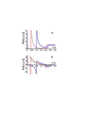
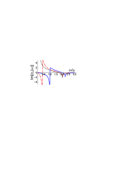
The real and imaginary parts of the conductivity at the temperature and two different are presented in Fig. 1. For the comparison the conductivity in the normal state is also shown. The frequency dependence of the transmission, reflection and absorption coefficients for the system with pairing and for the normal system are given in Fig. 2. One can see that the pairing results in the appearance of a sharp peak in the reflection and absorption at . This peak is accompanied with a deep minimum in the transmission. Below the gap () the system with pairing is completely transparent, while at it demonstrates significant absorption. In this range of frequencies the absorption coefficient decreases under increase in frequency up to . At that frequency a step-like increase of the absorption coefficient occurs. It is connected with opening of an additional channel of absorption caused by the transition between and states (8). Normal systems demonstrate similar step-like features at , but at much lower temperatures. At a step-like peculiarity is completely smeared out in the normal system (Fig. 2, left panel). In Fig. 2 the spectral characteristics are shown for and . One can see that lowering of results in a shift of the peak position. It the same time, the height and the width of the peaks remains practically unchanged. The computations show that the peaks caused by pairing are detectable already at .
The gap in the excitation spectrum may emerge not only due to electron-hole pairing, but due to the interlayer tunneling, as well. Absorption and reflection coefficients are not sensitive to the gap origin and the tunneling can mimic the effect of pairing. To identify the origin of the gap one can take into account that the gap caused by pairing depends on temperature. For the systems with pairing we expect a red shift of the peak and their disappearance under increase in temperature.
Strong concentration mismatch of graphene layers may also modify the spectral characteristics of double layer systems. Such a mismatch results in an appearance of two step-like singularity at and . The amplitude and the shape of these singularities differ significantly from ones for the peaks caused by pairing. Besides, in the normal system the step-like singularities are smeared out at rather small temperatures. It allows to distinguish the effect of the mismatch and of the pairing.
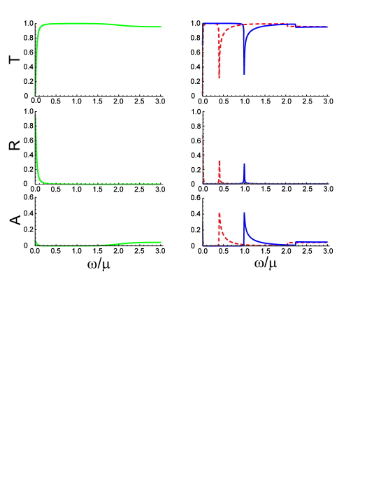
Concluding the section we note that a similar problem, an impact of an excitonic gap in the high-frequency conductivity, was considered in l5 with reference to a single graphene layer where the interaction may cause an opening of a gap in the quasiparticle spectrum in zero or in a finite magnetic field l6 . It was shown in l5 that the low part of the interband contribution to the conductivity cuts off at or whichever is the largest. For the bilayer system with the pairing we predict different behavior. The cutoff frequency is the minimum (not maximum) of and . In addition we find another step-like feature in the conductivity at the frequency .
Thus electron-hole pairing can be detected through an observation of strong reflection and absorption at the frequency . Taking , cm/s, and nm we evaluate meV and THz. This estimate shows that for the features we have described can be observed in the terahertz spectral range.
V Surface plasmon-polaritons in the system with pairing
Surface plasmon-polariton modes in graphene are now the subject of intensive study p1 ; p2 ; p3 ; p4 ; p5 . In particular, the interest to graphene is connected with the possibility of modifying the energy spectrum by external gates. The latter effect can be utilized in the plasmonic transformation opticsp6 . There are two kinds of surface plasmon-polariton waves in graphene, the TMp7 ; p8 and TEp9 ones. In the double layer system with the interlayer distance smaller than the inverse Fermi wave number two TM modes, the symmetric (optical) and antisymmetric (acoustic) onesp10 , and one (symmetric) TE mode can propagate. The question we consider is how the pairing influences the spectrum and damping of these modes.
V.1 TM modes
We consider a double layer graphene system in a vacuum. The graphene layers 1 and 2 are located in the and planes and separated by a spacer with the dielectric constant . The wave vector of the plasmon mode is directed along the axis. The electric field of the surface TM mode has the longitudinal () as well as the transverse () component, and the magnetic field has only the transverse () component. The electric and magnetic fields are exponentially decaying in both directions away from the graphene layers.
The presence of graphene layers is taken into account by the boundary conditions
| (44) | |||||
| (45) |
where and are the intralayer and interlayer conductivity, and is the parallel current (counterflow) conductivity. The latter quantities are expressed through the response functions :
| (46) |
The solution of Maxwell equations with the boundary conditions (44) yields the dispersion equations for the symmetric () and antisymmetric () TM modes:
| (47) |
| (48) |
where and .
In a wide range of frequencies the wave vector of the surface TM mode is much larger than the wave vector of an electromagnetic wave with the same frequency in a free space (). This condition is violated only for the symmetric mode at very small . This range of is not considered here. Implying also that we replace and in the dispersion equations (47), (48) with and reduce Eqs. (47), (48) to the form
| (49) |
where
| (50) |
are the two-dimensional(2D) dielectric functions. The functions determine the screening of the scalar potentials of the test charges and located in the graphene layers 1 and 2 one above the other. The functions (50) can be presented in the form
| (51) |
where
| (52) |
One can see that Eq. (51) corresponds to the random phase approximation for the dielectric functions.
Eq. (49) determines the dispersion of 2D plasmons. The difference between 2D plasmons and three-dimensional (3D) plasmons is the following. 3D plasmons are the longitudinal excitations of the electric field. Plasmons in 2D conductors in a 3D space are TM waves. The electric field of that wave has the longitudinal as well as the transverse component. The magnetic field is also nonzero but small in the limit .
We specify the case and consider the range of wave vectors . Expanding in the small parameter and neglecting the higher order terms we obtain
| (53) |
| (54) |
Let us first analyze the dispersion equation for the symmetric TM wave. According to Eqs. (49) and (53) this mode can propagate in the frequency range where . The qualitative analysis can be done by replacing with . Then from Fig. 1 we see that in the system with the pairing at the dispersion equation may have two solutions, one is in the range , and the other, in the range . The real part of determines Landau damping. Since is extremely small at one can expect that the low frequency solution corresponds to weakly damped plasmons. For the real part of conductivity is rather large and the high frequency solution will correspond to strongly damped plasmons.
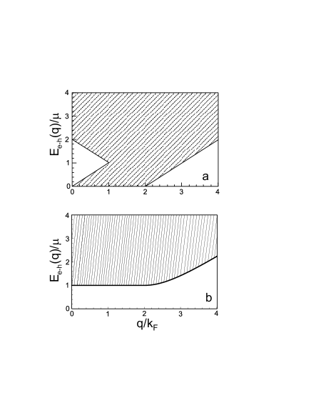
The influence of pairing on Landau damping can be understood from the spectrum of electron-hole single particle excitations. In the system with pairing all states with negative energies () are filled at , and all states with positive energies () are empty. Therefore, the continuum of electron-hole excitations is determined by the inequality
| (55) |
where the minimum is taken over all , and . It follows from this inequality that . In the normal system the electron-hole excitation continuum starts from . Fig. 3 demonstrates the modification of the electron-hole excitation continuum under the pairing. One can see that in the paired state Landau damping for the modes with energies is suppressed, while the modes with may suffer from a strong damping.
We compute the spectrum of the symmetric TM wave from the equation
| (56) |
where is given by Eq. (53) in which the dependence of on is taken into account. The damping rate is evaluated as
| (57) |
where is the solution of Eq. (56). Since Eqs. (56), (57) are valid at small damping we do not consider the solutions of Eq. (56) with .
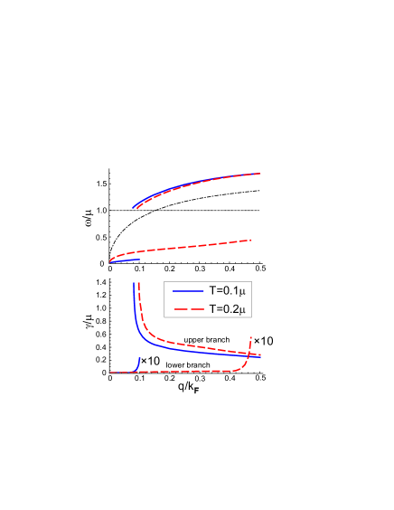
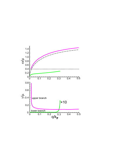
The results of computation for at and are presented in Fig. 4. One can see that in the state with the pairing the symmetric TM mode splits into two branches (the spectrum in the normal state is also shown in Fig. 4). In the long wavelength range the lower branch is a weakly damped one. There is a critical wave vector above which the solution of Eq. (56) that corresponds to the lower branch disappears. At approaching the damping rate for the lower branch increases sharply. Under increase in temperature the frequency of this mode and the critical wave vector grows up . The lower branch is a thermally activated mode. At this mode does not exist. It can be seen from the explicit expression for the response function (Eq. (38)). At this response function is real and negative at . Therefore and Eq. (56) has no solution in the frequency range at zero temperature. The behavior of the lower mode allows considering it as one connected with plasmon oscillations of the normal component decoupled from the superfluid one.
The frequency of the upper branch is restricted from below by the inequality . The damping rate for this mode is much higher than for the lower branch. This branch exists in the wave vector range . At close to the frequency of this mode approaches and its damping rate increases sharply (the mode becomes overdamped).
In Fig. 5 the spectrum and the damping rate for the lower and upper branches at and are shown. Comparing Fig. 5 and Fig. 4 we conclude that lowering of (at the same ) results in an expansion of the wave vector range for two branches and in a decrease of the frequency and the damping rate of the upper branch.
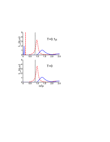
The plasmon mode spectrum can also be extracted from the energy loss function
| (58) |
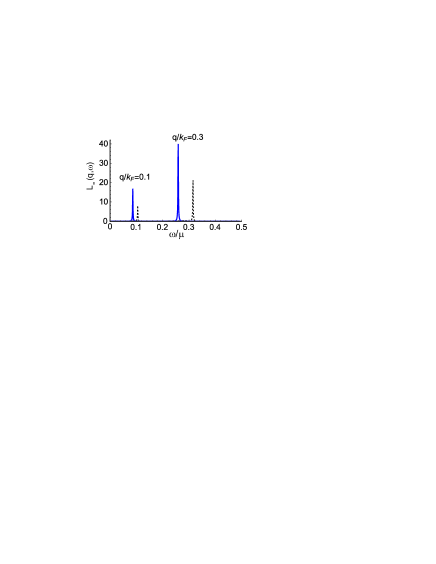
This function determines the losses of energy of a pair of test charges oscillating with the frequency located in the adjacent graphene layers opposite to each other. The losses are connected with the excitation of plasmons at this frequency. A sharp peak in the loss function corresponds to a weakly damped plasmon mode. In Fig. 6 the dependence of on at fixed is presented for and . At this dependence contains a sharp peak that corresponds to the lower mode and a wide peak that corresponds to the upper mode. The positions of the peaks depend on . At the peak that corresponds to the lower mode disappears, while the upper mode peak remains unchanged. There is only one peak at . It corresponds to the symmetric TM mode in the normal state. The behavior of the loss function demonstrates splitting of the TM wave into the lower and upper branches. The lower one is a weakly damped and thermally activated mode. The upper one is a strongly damped mode, and practically unsensitive to the temperature in the temperature range considered.
Concluding this analysis we note that the splitting of the plasmon mode into a number of branches may also for the system is subjected by a strong magnetic field directed perpendicular to the graphene layers (without electron-hole pairing)b2 .
Let us now switch to the antisymmetric mode. The gauge-invariant response function is given by Eq. (24) with the renormalized vertex function (30). The result of computation can be presented in the form
| (59) |
where the first term corresponds to the bare vertex approximation
| (60) | |||
| (61) |
and the second term is caused by the renormalization of the bare vertex functions (30)
| (62) |
At the second term in Eq. (59) vanishes. Therefore, the static response function is gauge invariant in the bare vertex approximation. The conductivity is determined by Eq. (46). In the limit this equation gives the uniform conductivity . The right hand side of Eq. (46) has a finite limit if . At the quantity compensates the terms proportional to in , and in this limit the expression for (Eq. (59)) coincides with one for (Eq. (38)). Using the explicit expression (38) one can show analytically that indeed . In other words, the vertex function in the form Eq. (30) ensures the applicability of Eq. (46). In the contrary, computations with the bare vertex instead of the dressed one would yield an unphysical answer for .
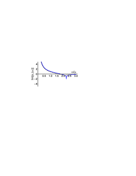
As above, for the qualitative analysis one can neglect the dependence of on in Eq. (54). The dependence computed from Eqs. (46) and (59) is shown in Fig. 7. One can see that the imaginary part of remains almost unchanged under the pairing and we expect only an inessential impact of the pairing on the spectrum of the antisymmetric TM mode.
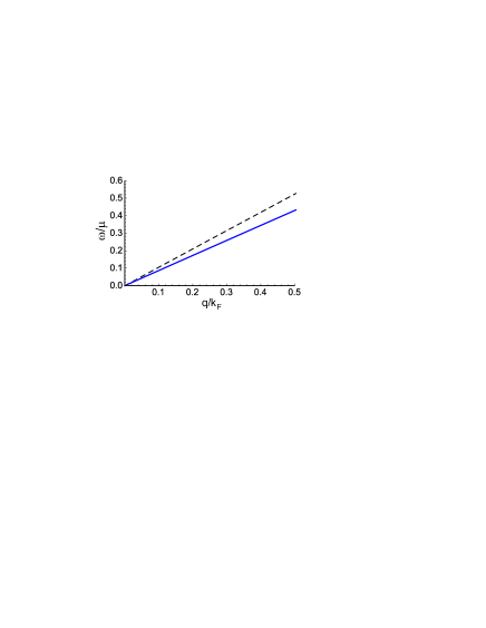
The spectrum of the antisymmetric TM mode computed from the equation with given by Eq. (54) is shown in Fig. 8. The parameters and are used for the computations. Fig. 8 shows that the antisymmetric TM mode remains the acoustic one in the state with the pairing and its velocity slightly reduces comparing to one in the normal state. In Fig. 9 the loss function is presented. Fig. 9 demonstrates that the antisymmetric mode is a weakly damped one in the normal as well as in the paired state. We remind that the renormalized vertex function (30) was obtained in the limit and its applicability at frequencies is questionable.
The fact that the pairing does not influence the antisymmetric TM mode can be understood as follows. This mode corresponds to out-of-phase oscillations of electron densities in graphene layers. Out-of-phase oscillations in electron densities are equivalent to in-phase oscillations in electron and hole densities. It is quite natural that the electron-hole pairing does not suppress such oscillations.
V.2 TE modes
Surface TE waves with the wave vector directed along the axis have the transverse electric component and the longitudinal as well as the transverse magnetic component. The boundary conditions for the tangential component of the magnetic field are
| (63) | |||||
| (64) |
Maxwell equations with the boundary conditions (63) yield the dispersion equations for the TE waves:
| (65) |
| (66) |
where and . Eq. (65) corresponds to the symmetric TE wave, and Eq. (66), to the antisymmetric TE wave.
At (no graphene layers) and the general Eqs. (65), (66) have a number of solutions which correspond to the symmetric and antisymmetric waveguide modes. At only the lowest symmetric mode survives. The presence of graphene layers influences only the modes with the phase velocities close to the light velocity . We restrict our analysis with frequencies comparable or smaller than the chemical potential . The mode with the phase velocity and the frequency has the wave vector . Since the pairing occurs at , the strong inequality is fulfilled. In this limit the real part of Eq. (65) is reduced to
| (67) |
where is the fine structure constant, is the conductivity normalized to , and is the material parameter. In Eq. (67) we take into account that is in 3 orders smaller than and replace the finite wave vector conductivity with the uniform conductivity . Eq. (67) determines the phase velocity as the function of . Eq. (67) has a solution in the frequency range, where . For typical parameters (, , and ) the constant is very small () and it can be neglected. In fact, the TE wave frequency range is determined by the same condition as one for the monolayer graphene ().
In the normal state the TE mode exists only at . One can see from Fig. 1b that the pairing opens the low frequency window for the TE mode. At temperature the condition is fulfilled for (see Fig. 10) and the lower edge goes to zero.
VI Conclusion
In conclusion, we have shown that the electron-hole pairing significantly changes spectral properties of double layer graphene systems in the terahertz range. The pairing causes the appearance of sharp high peaks in the absorption and reflection at the frequency and a rather large (much larger than in an undoped graphene) absorption at .
The pairing influences essentially the surface symmetric TM mode. This mode splits into the lower and upper branches. The lower branch has the frequency . It is practically undamped and appears only at nonzero temperatures in the long wavelength range. The spectrum of the lower branch is strongly temperature dependent. The upper branch frequency is in the range , and this mode is strongly damped.
The influence of pairing on the antisymmetric TM mode is inessential.
It is established that in the paired state a low frequency TE mode can propagate. In the normal state the frequency range for such a mode is restricted from below by the inequality . In the paired system the additional frequency window opens, where goes to zero at .
Other Dirac double layer systems such as thin topological insulator plates, double layer silicene, germanene and -graphyne structures will demonstrate the same behavior. We also expect qualitatively the same features in double layer electron-hole systems made of a pair of bilayerbil or few-layer graphene mult sheets.
The appearance of additional peaks in the transmission, reflection, and absorption spectra of double layer graphene systems would be a hallmark of the electron-hole pairing. A strong modification of the spectrum of an optical TM mode with temperature can be used in plasmonics for creating transformation optic devices with a thermal control.
References
- (1) S. I. Shevchenko, Fiz. Nizk. Temp. 2, 505 (1976) [Sov. J. Low Temp. Phys. 2, 251 (1976)].
- (2) Yu. E. Lozovik, V. I. Yudson, Zh. Eksp. Teor. Fiz. 71, 738 (1976) [Sov. Phys. JETP 44, 389 (1976)].
- (3) A. F. Croxall, K. Das Gupta, C. A. Nicoll, M. Thangaraj, H. E. Beere, I. Farrer, D. A. Ritchie, M. Pepper, Phys. Rev. Lett. 101, 246801 (2008).
- (4) J. A. Seamons, C. P. Morath, J. L. Reno, M. P. Lilly, Phys. Rev. Lett. 102, 026804 (2009).
- (5) A. Gamucci, D. Spirito, M. Carrega, B. Karmakar, A. Lombardo, M. Bruna, L. N. Pfeiffer, K. W. West, A. C. Ferrari, M. Polini, V. Pellegrini, Nature Communications 5, 5824 (2014).
- (6) M. P. Mink, H. T. C. Stoof, R. A. Duine, M. Polini, G. Vignale, Phys. Rev. Lett. 108, 186402 (2012).
- (7) M. P. Mink, H. T. C. Stoof, R. A. Duine, M. Polini, G. Vignale, Phys. Rev. B 88, 235311 (2013).
- (8) H. A. Fertig, Phys. Rev. B 40, 1087 (1989).
- (9) D. Yoshioka, A. H. MacDonald, J. Phys. Soc. Jpn. 59, 4211 (1990).
- (10) K. Moon, H. Mori, K. Yang, S. M. Girvin, A. H. MacDonald, L. Zheng, D. Yoshioka, S. C. Zhang, Phys. Rev. B 51, 5138 (1995).
- (11) M. Kellogg, J. P. Eisenstein, L. N. Pfeiffer, K. W. West, Phys. Rev. Lett. 93, 036801 (2004).
- (12) R. D. Wiersma, J. G. S. Lok, S. Kraus, W. Dietsche, K. von Klitzing, D. Schuh, M. Bichler, H.-P. Tranitz, W. Wegscheider, Phys. Rev. Lett. 93, 266805 (2004).
- (13) E. Tutuc, M. Shayegan, D. A. Huse, Phys. Rev. Lett. 93, 036802 (2004).
- (14) D. Nandi, A. D. K. Finck, J. P. Eisenstein, L. N. Pfeiffer, K. W. West, Nature 488, 481 (2012).
- (15) H. Min, R. Bistritzer, J.-J. Su, A. H. MacDonald, Phys. Rev. B 78, 121401(R) (2008).
- (16) Yu. E. Lozovik, A. A. Sokolik, Pis ma Zh. Eksp. Teor. Fiz. 87, 61 (2008) [JETP Lett. 87, 55 (2008)].
- (17) B. Seradjeh, H. Weber, M. Franz, Phys. Rev. Lett. 101, 246404 (2008).
- (18) M. Y. Kharitonov, K. B. Efetov, Phys. Rev. B 78, 241401(R) (2008).
- (19) M. Y. Kharitonov, K. B. Efetov, Semicond. Sci. Technol. 25, 034004 (2010).
- (20) I. Sodemann, D. A. Pesin, A. H. MacDonald, Phys. Rev. B 85, 195136 (2012).
- (21) Yu. E. Lozovik, S. L. Ogarkov, A. A. Sokolik, Phys. Rev. B 86, 045429 (2012).
- (22) Nathanael J. Roome, J. David Carey, ACS Appl. Mater. Interfaces 6, 7743 (2014).
- (23) Pere Miro, Martha Audiffred, Thomas Heine, Chem. Soc. Rev. 43, 6537 (2014).
- (24) Jinying Wang, Shibin Deng, Zhongfan Liu, Zhirong Liu, National Science Review 2, 22 (2015).
- (25) J. L. Plawsky, J. K. Kim, E. F. Schubert, Mater. Today 12, No. 6, 36 (2009).
- (26) W. Volksen, R. D. Miller, G. Dubois, Chem. Rev. 110, 56 (2010).
- (27) B. Seradjeh, J. E. Moore, M. Franz, Phys. Rev. Lett. 103, 066402 (2009).
- (28) D. K. Efimkin, Yu. E. Lozovik, A. A. Sokolik, Phys. Rev. B 86, 115436 (2012).
- (29) L. Dell’Anna, A. Perali, L. Covaci, D. Neilson, Phys. Rev. B 92, 220502(R) (2015).
- (30) O. L. Berman, Y. E. Lozovik, G. Gumbs, Phys. Rev. B 77, 155433 (2008).
- (31) Z. G. Koinov, Phys. Rev. B 79, 073409 (2009).
- (32) D. V. Fil and L. Yu. Kravchenko , Low Temp. Phys. 35, 712 (2009) [Fiz. Nizk. Temp. 35, 904 (2009)].
- (33) A. A. Pikalov and D. V. Fil, Nanoscale Res. Lett. 7, 145 (2012).
- (34) O. L. Berman, R. Y. Kezerashvili, K. Ziegler, Phys. Rev. B 85, 035418 (2012).
- (35) A. Stern, B. I. Halperin, Phys. Rev. Lett. 88, 106801 (2002).
- (36) K. V. Germash, D. V. Fil, Phys. Rev. B 91, 115442 (2015).
- (37) D. K. Efimkin and Yu. E. Lozovik, Phys. Rev. B 88, 085414 (2013).
- (38) Y. Nambu, Phys. Rev. 117, 648 (1960).
- (39) M. P. Mink, H. T. C. Stoof, R. A. Duine, A. H. MacDonald, Phys. Rev. B 84, 155409 (2011).
- (40) J. R. Schrieffer, Theory of superconductivity, Benjamin, New York (1964).
- (41) P. W. Anderson, Phys. Rev. 112, 1900 (1958).
- (42) N. N. Bogoliubov, V. V. Tolmachev, D. V. Shirkov, A new method in the theory of superconductivity, edited by N. N. Bogoliubov, Consultants Bureau, New York (1959).
- (43) V. P. Gusynin, S. G. Sharapov, J. P. Carbotte, Int. J. Mod. Phys. B 21, 4611 (2007).
- (44) R. R. Nair, P. Blake, A. N. Grigorenko, K. S. Novoselov, T. J. Booth, T. Stauber, N. M. R. Peres, A. K. Geim, Science 320, 1308 (2008).
- (45) M. I. Katsnelson, Graphene: Carbon in two dimensions, Cambridge University Press (2012).
- (46) T. Stauber, N. M. R. Peres, A. K. Geim, Phys. Rev. B 78, 085432 (2008).
- (47) L. A. Falkovsky, A. A. Varlamov, Eur. Phys. J. B 56, 281 284 (2007).
- (48) A. Principi, M. Polini, G. Vignale, Phys. Rev. B 80, 075418 (2009).
- (49) V. P. Gusynin, S. G. Sharapov, J. P. Carbotte, Phys. Rev. Lett. 96, 256802 (2006).
- (50) E. V. Gorbar, V. P. Gusynin, V. A. Miransky, I. A. Shovkovy, Phys. Rev. B 66, 045108 (2002).
- (51) T. Low, P. Avouris, ACS Nano 8(2), 1086 (2014).
- (52) F. Javier Garcia de Abajo, ACS Photonics 1(3), 135 (2014).
- (53) T. Stauber, J. Phys.: Condens. Matter 26, 123201 (2014).
- (54) Yu. V. Bludov, A. Ferreira, N. M. R. Peres, M. I. Vasilevskiy, Int. J. Mod. Phys. B 27, 1341001 (2013).
- (55) M. Jablan, M. Soljacic, H. Buljan, Proceedings of the IEEE 101, 1689 (2013).
- (56) A. Vakil, N. Engheta, Science 332 No 6035, 1291 (2011).
- (57) O. Vafek, Phys. Rev. Lett. 97, 266406 (2006).
- (58) E. H. Hwang, S. Das Sarma, Phys. Rev. B 75, 205418 (2007).
- (59) S. A. Mikhailov, K. Ziegler, Phys. Rev. Lett. 99, 016803 (2007).
- (60) E. H. Hwang, S. Das Sarma, Phys. Rev. B 80, 205405 (2009).
- (61) O. L. Berman, G. Gumbs, Yu. E. Lozovik, Phys. Rev. B 78, 085401 (2008).
- (62) A. Perali, D. Neilson, A. R. Hamilton, Phys. Rev. Lett. 110, 146803 (2013).
- (63) M. Zarenia, A. Perali, D. Neilson, F. M. Peeters, Sci. Rep. 4, 7319 (2014).