Theoretical and computational analysis of second- and third-harmonic generation in periodically patterned graphene and transition-metal dichalcogenide monolayers
Abstract
Remarkable optical and electrical properties of two-dimensional (2D) materials, such as graphene and transition-metal dichalcogenide (TMDC) monolayers, offer vast technological potential for novel and improved optoelectronic nanodevices, many of which relying on nonlinear optical effects in these 2D materials. This article introduces a highly effective numerical method for efficient and accurate description of linear and nonlinear optical effects in nanostructured 2D materials embedded in periodic photonic structures containing regular three-dimensional (3D) optical materials, such as diffraction gratings and periodic metamaterials. The proposed method builds upon the rigorous coupled-wave analysis and incorporates the nonlinear optical response of 2D materials by means of modified electromagnetic boundary conditions. This allows one to reduce the mathematical framework of the numerical method to an inhomogeneous scattering matrix formalism, which makes it more accurate and efficient than previously used approaches. An overview of linear and nonlinear optical properties of graphene and TMDC monolayers is given and the various features of the corresponding optical spectra are explored numerically and discussed. To illustrate the versatility of our numerical method, we use it to investigate the linear and nonlinear multiresonant optical response of 2D-3D heteromaterials for enhanced and tunable second- and third-harmonic generation. In particular, by employing a structured 2D material optically coupled to a patterned slab waveguide, we study the interplay between geometric resonances associated to guiding modes of periodically patterned slab waveguides and plasmon or exciton resonances of 2D materials.
pacs:
(42.25.Fx) Diffraction and scattering, (42.65.-k) Nonlinear optics, (78.67.Wj) Optical properties of graphene, (78.68.+m) Optical properties of surfaces.I Introduction
Since its first isolation, preparation, and theoretical description [1, 2, 3], graphene, a monolayer of carbon atoms distributed in a hexagonal lattice, has attracted a tremendous amount of interest in science and engineering due primarily to its outstanding physical properties and potential for novel applications. Graphene was shown to have remarkable mechanical strength [4, 5, 6] and extremely high thermal conductivity [7], making it a particularly appealing materials platform for nano-electromechanical applications and management of thermal processes in nanoelectronic circuits [5, 8]. In addition, the high carrier mobility of graphene enhances its potential for applications to high-frequency electronics [9, 10, 11]. These and other remarkable properties of graphene have spurred new research into and development of new two-dimensional (2D) materials, such as hexagonal boron nitride (h-BN), silicene (a monolayer of silicon), and transition-metal dichalcogenide (TMDC) monolayers [12, 13, 14, 15], each with their own array of unique physical properties.
One additional compelling aspect of 2D materials (2DMs) is closely related to their optical properties. Graphene, for example, is nearly transparent at optical frequencies, exhibiting absorption of only about 2.3% [16], which suggests it barely interacts with light. This optical transparency and the earlier mentioned electro-mechanical properties make graphene a promising new material for flexible optical devices [17] (e.g., touch screens). Moreover, graphene based structures can provide an alternative to conventional metallo-dielectric structures to spatially confine and guide light at the nanoscale, a research direction actively pursued in the emerging field of graphene nanoplasmonics [18, 19, 20, 21, 22, 23, 24, 25, 26, 27].
In addition to these linear physical properties, the nonlinear optical properties of graphene and other 2D materials have attracted increased attention. Graphene, as a centrosymmetric material, exhibits large third-harmonic generation (THG) [28, 29], strong optical Kerr nonlinearity [30], and induced second-order nonlinearity [31, 32, 33] in a single atomic layer. This allows one to employ graphene in active photonic devices with improved functionality, including ultra-compact modulators, optical limiters, frequency converters, and photovoltaic and photoresistive devices [17, 28, 29, 31, 30, 34]. In a complementary fashion, TMDC monolayers are semiconducting materials, which renders them particularly suitable to be employed in nanoscale transistors and saturable absorbers [35, 36], and have non-centrosymmetric atomic lattice and hence allow even-order nonlinear optical processes [37, 38, 39, 40]. The implementation of these linear and nonlinear optical properties into applications, however, requires advances in nanofabrication and experimental techniques [17, 41, 42], theoretical models, and numerical methods for modeling of devices incorporating 2D materials.
There is a multitude of numerical methods for computational study of optical structures and devices comprising regular, three-dimensional (3D) materials [43, 44], and they can in principle be used for modeling 2D materials, too. This is customarily done by defining an effective thickness of the material and incorporating the 2DM into the computational algorithm simply as a very thin layer of 3D material [45, 46, 47]. This computational approach, albeit simple and easy to implement, has a serious drawback, namely it relies on an obviously ambiguous quantity, the thickness of the monolayer. Moreover, this thickness is typically orders of magnitude smaller than the other characteristic lengths of the photonic structure and the operating wavelength, leading to a large length-scale imbalance that is detrimental to the effectiveness of the spatial discretization. These issues result in potentially reduced accuracy, increased computational cost, and numerical artefacts that are difficult to avoid [48, 49]. It is hence desirable to treat the sources of the optical effects pertaining to the 2DM as confined to a 2D manifold, i.e. as induced by a surface conductivity [48, 50, 51].
The numerical method proposed here follows this approach and implements it in the context of the rigorous coupled-wave analysis (RCWA) method, a modal frequency domain method for modeling periodic optical structures [52, 53, 54]. However, in addition to previous work on handling 2DMs by means of Fourier series expansion methods [49, 55], we also model nonlinear optical effects in 2D materials, in particular second-harmonic generation (SHG) and THG, and provide the mathematical formulation for arbitrary nonlinear optical processes. In addition, the method introduced in this work allows one to describe structured 2D materials, which themselves can be embedded in inhomogeneous 3D optical structures.
The remainder of this paper introduces the general periodic optical system under consideration in Section II and gives a detailed overview of linear and nonlinear optical properties of different 2DMs in Section III. Section IV provides the mathematical formulation for higher-harmonic generation in patterned 2DMs based on the RCWA and introduces the inhomogeneous scattering matrix formalism for multilayered 3D structures. This is followed by Section V, where the validation and benchmarking of the numerical method is performed, using as test problems one-dimensional (1D) and 2D periodic structures. Applications of the proposed numerical method are presented and discussed in Section VI, where we also investigate different resonant mechanisms to enhance the nonlinear optical response of 2D-3D heteromaterials containing TDMC monolayers and nanostructured graphene. Finally, the main conclusions are drawn and an outlook towards future work is given in Section VII.
II Photonic system: Geometry and materials parameters
The computational method introduced in this article is designed for a very general physical setting, namely periodically patterned photonic structures that contain both bulk and 2D optical materials. Our numerical method accurately describes the physics of such photonic structures by incorporating in the numerical algorithm the relevant linear and nonlinear optical effects pertaining to 2D materials. Equally important, since the nonlinear optical response of different 2D materials contained by the photonic structure is described via a generic nonlinear polarization, this computational method can be used to investigate a multitude of nonlinear optical effects, including SHG, sum- and difference-frequency generation, THG, and four-wave mixing.
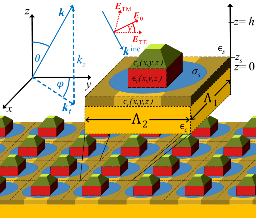
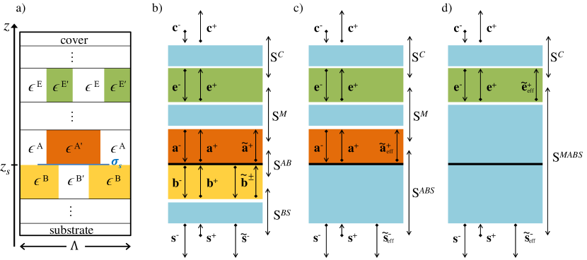
The geometric setting and important nomenclature used in the presentation of our numerical method are introduced in what follows. Thus, consider the generic multilayer, periodic structure presented in Fig. 1. The bird’s-eye view in Fig. 1 depicts the unit cell of a 2D-periodic structure with periods and , with the corresponding grating vectors, and , laying in the -plane. It consists of several bulky, periodically structured regions with relative electric permittivity, , which will be called bulk-layers, or simply layers. The periodic structure is sandwiched in-between semi-infinite homogeneous cover and substrate layers with relative permittivity, and , respectively. In addition, the structure can comprise 2DM sheets, or simply sheets, located at , which are assumed to lay in the -plane between two bulk-layers. Each sheet is made of homogeneous or periodically patterned 2DMs and is described by its surface conductivity distribution, .
This periodic structure is excited by an incident harmonic plane wave with the electric field given by:
| (1) |
where is the angular frequency, is the in-plane component of the position vector, and are the in-plane and normal components of the wave vector of the incident wave in the cover, respectively, with being the wavenumber in the cover region and is the speed of light. The polarization state of the incoming plane wave is described by the field components in the transverse electric (TE) and transverse magnetic (TM) configurations, namely and , respectively, such that is determined by the polarization angle, .
In the rigorous coupled-wave analysis, the underlying algorithm on which our computational method is built, oblique structures or devices consisting of several periodic layers are approximated in a staircasing manner (see Ref. [56]). To be more specific, the structure is sliced into thin and -invariant bulk-layers, the optical response of each layer is calculated, and then the combined response of all layers is determined by properly incorporating the inter-layers optical coupling described in Section IV.4. Before this algorithm is derived thoroughly in Section IV, the optical properties of 2DMs are introduced and formalized mathematically in the next section.
III Linear and nonlinear optical properties of 2D materials
Understanding the physics of 2DMs is a rather recent endeavor and as such a comprehensive characterization of their linear and nonlinear optical properties is only emerging. In particular, a complete knowledge of the frequency dependence of the linear and nonlinear optical constants is a prerequisite for a rigorous computational description of the optical response of these materials. Theoretical calculations [57, 58, 29, 37] and experimental investigations [59, 60, 28] are beginning to fill in this gap, a summary of the results of these studies being briefly outlined in this section.
III.1 Linear optical properties of 2D materials
Since graphene and other 2DMs are physical systems consisting of a single atomic layer, their electromagnetic properties are conveniently characterized by surface quantities. For example, in the case of graphene, the optical properties are described by the sheet conductance (sometimes simply called conductivity), which in the random-phase approximation and zero temperature conditions can be expressed as [57, 61]:
| (2) |
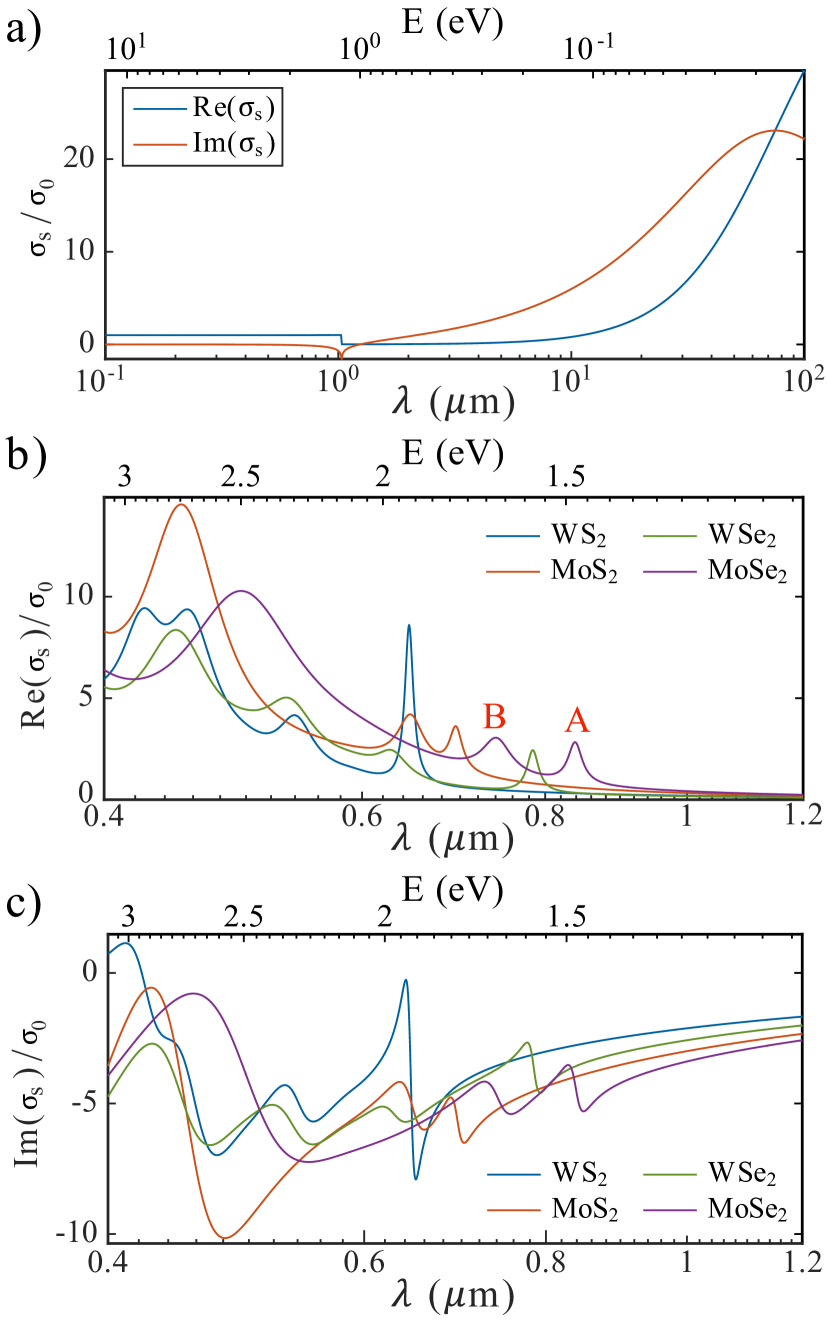
Here, is the universal dynamic conductivity of graphene, denotes the elementary charge, the Fermi level, the reduced Planck constant, the relaxation time and is the Heaviside step function. The values of the Fermi level and relaxation time used throughout this study are and , respectively. The dispersion of for graphene is shown in Fig. 2(a).
| () | () | () | () | () | () | () | () | () | () | () | () | |
|---|---|---|---|---|---|---|---|---|---|---|---|---|
| 1 | 2.009 | 1.928 | 0.032 | 1.654 | 0.557 | 0.036 | 1.866 | 0.752 | 0.045 | 1.548 | 0.648 | 0.043 |
| 2 | 2.204 | 0.197 | 0.250 | 2.426 | 5.683 | 0.243 | 2.005 | 1.883 | 0.097 | 1.751 | 1.302 | 0.097 |
| 3 | 2.198 | 0.176 | 0.161 | 2.062 | 1.036 | 0.115 | 2.862 | 36.89 | 0.383 | 2.151 | 4.621 | 0.537 |
| 4 | 2.407 | 0.142 | 0.112 | 2.887 | 16.11 | 0.344 | 2.275 | 10.00 | 1.000 | 2.609 | 37.40 | 0.582 |
| 5 | 2.400 | 2.980 | 0.167 | 2.200 | 1.500 | 0.300 | 3.745 | 100.0 | 0.533 | 3.959 | 121.4 | 0.896 |
| 6 | 2.595 | 0.540 | 0.213 | 2.600 | 1.500 | 0.300 | - | - | ||||
| 7 | 2.644 | 0.050 | 0.171 | 3.800 | 70.00 | 0.700 | - | - | ||||
| 8 | 2.831 | 12.60 | 0.266 | 5.000 | 80.00 | 0.700 | - | - | ||||
| 9 | 3.056 | 8.765 | 0.240 | - | - | - | ||||||
| 10 | 3.577 | 29.99 | 1.196 | - | - | - | ||||||
| 11 | 5.078 | 49.99 | 1.900 | - | - | - | ||||||
| 12 | 5.594 | 79.99 | 2.510 | - | - | - | ||||||
The sheet conductance contains the intraband (Drude) contribution, described by the first term in the r.h.s. of Eq. (2), and the interband component given by the next two terms. A more complete model valid at finite temperature can be used (see Refs. [57, 61, 62]); however, the model described by Eq. (2) already captures the main features of graphene conductivity, most notable being the possibility of tuning by changing the Fermi level via chemical doping or applying a gate voltage.
In many numerical methods pertaining to computational electromagnetics it is more convenient to work with bulk rather than surface quantities and therefore one often introduces bulk equivalents of the surface quantities. In particular, instead of the sheet conductance, , one uses a bulk conductivity, , where is the effective thickness of the 2DM. This approach can oftentimes create confusion due to the ambiguity contained in the definition of the thickness of an atomic monolayer. Moreover, the electromagnetic properties of 2DMs can alternatively be described by the electric permittivity, , which is related to the optical conductivity via the following relation:
| (3) |
In the case of TMDC monolayer materials, we describe their relative electric permittivity, , as a superposition of Lorentzian functions:
| (4) |
where , , and are the oscillator strength, resonance frequency, and spectral width of the th oscillator, respectively. The values of the model parameters for the four considered TMDC monolayers were determined by fitting Eq. (III.1) to the experimental data provided in Ref. [59] and are presented in Table 1 in terms of , , and . Note that the permittivity given by Eq. (III.1) fulfils the Kramers-Kronig relation; however, the numerical fitting is less accurate for () due to the limited range of the available experimental data.
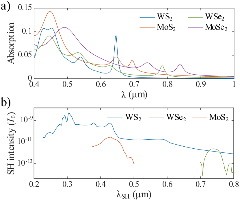
The spectra of , a physical quantity related to the optical absorption in the material, and are depicted in Figs. 2(b) and 2(c), respectively. For each TMDC, exhibits spectral peaks at wavelengths specific to the particular 2DM: the absorption peaks of with highest and second highest wavelength for each material (shown for MoSe2 as and , respectively) correspond to low-energy interband transitions at the -point of the first Brillouin zone due to splitting of the valence-band by spin-orbit coupling, whereas peaks at lower wavelengths correspond to higher energy interband transitions [59].
III.2 Nonlinear optical properties of 2D materials
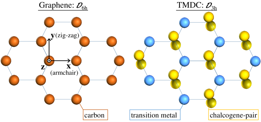
The lattices of graphene and TMDC monolayers belong to different space symmetry groups, which means that each of these materials requires a separate treatment. The graphene lattice belongs to the space group, as illustrated in Fig. 3, which means that graphene is a centrosymmetric material and thus SHG is a forbidden nonlinear optical process. On the other hand, THG is an allowed, particularly strong process in graphene [28, 29], which makes it a suitable material for nonlinear optical applications. By contrast, TMDC monolayers belong to the space group [63] so that in this case SHG is the lowest-order nonlinear optical process.
The nonlinear optical response of graphene can be described by using the nonlinear optical conductivity tensor, , which relates the nonlinear surface current density, , and the electric field, , at the fundamental frequency (FF). Thus, if we assume that the graphene sheet lies in the -plane at =0, the nonlinear current density, , can be written as:
| (5) |
where is the position vector lying in the graphene plane. Then, the nonlinear surface current density can be written as:
| (6) |
where is the electric field component lying in the plane of graphene. In this description [29], the nonlinear current density lies in the plane of graphene and only depends on the tangential field components. As a result, and . A formula for , derived under the assumptions that electron-electron and electron-phonon scattering as well as thermal effects can be neglected, has been recently derived in Ref. [29] and reads:
| (7) |
In this equation, derived using perturbation theory, ,
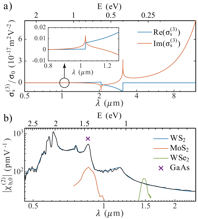
and is the Fermi velocity, with being the nearest-neighbor distance between carbon atoms in graphene and is the nearest-neighbor coupling constant. Figure 4(a) depicts and additionally highlights the lowest spectral peak at in the inset of the figure.
Similarly to the linear case, one can introduce a “bulk” nonlinear conductivity, . This nonlinear conductivity is particularly useful in experimental investigations of nonlinear optics of graphene because it is related to an effective bulk third-order nonlinear susceptibility, , the physical quantity that is usually measured experimentally. Using the fact that for harmonic fields , where is the nonlinear polarization, one can easily show that
| (8) |
where is the frequency at the third-harmonic (TH), with being the fundamental frequency.
In contrast to graphene, TMDC monolayers are non-centrosymmetric (see Fig. 3) and therefore SHG is allowed [64, 65]. Based on the symmetry properties of their space group, , it can be shown that the structure of their quadratically nonlinear susceptibility tensor, , yields only one independent, non-vanishing component [64, 37, 38]:
| (9) |
where is the armchair direction of the monolayer and the orthogonal zig-zag-direction. The nonlinear surface conductivity tensor, , has the same structure and is related to the nonlinear susceptibility via a relation similar to Eq. (8):
| (10) |
being the second-harmonic (SH) frequency.
Numerical values for the effective thickness of the four TMDC monolayer materials are taken from Ref. [59] and are presented in Table 1. Although the tensorial structure expressed in Eq. (9) already qualitatively determines the nonlinear surface current,
| (11) |
the particular value of (and hence that of ) is of practical importance. Reliable values over a certain spectral range exist for [37], [38, 39], and [40] and are depicted in Fig. 4(b). Despite these materials consisting of just a single atomic layer, the largest values of , , and , respectively, have comparable magnitude to that of GaAs, , a medium with strong bulk quadratic susceptibility [65, 66].
It is also instructive to compare the strength of the SHG in TMDC monolayer materials to that in noble metals, as in both cases the SH is generated largely in a single atomic layer. To this end, we introduce a surface quadratic nonlinear susceptibility tensor, , which we then compare to the surface quadratic nonlinear susceptibility tensor of Au and Ag. The highest value of of is and is hence comparable to the dominant component, , for Ag and Au, i.e. and [67], respectively.
IV Higher-harmonic generation in periodically patterned 2D materials
This section will introduce a numerical method for calculating the nonlinear optical interaction of light with periodic structures consisting of 2DMs embedded in dielectric or metallic patterned media. Nonlinear optical effects in the bulk part of periodic structures are not considered in this article, as there already exist numerical formulations that are compatible with [68, 69, 70] or complementary to [71] the proposed method to accurately calculate these bulk nonlinear optical effects.
To this end, the undepleted pump approximation will be used as a means to introduce the nonlinear optical interactions in the governing Maxwell equations (MEs). Since the basis of the proposed numerical method is the RCWA, this method will be briefly revisited and the necessary mathematical formalism derived. Then, a modified boundary condition for interfaces incorporating conductive, potentially nonlinear 2DMs, is considered and a numerically stable -matrix algorithm for propagation of nonlinear fields generated by the monolayers of 2DMs in multilayered periodic structures is derived to complete the proposed algorithm. Importantly, the thickness of the 2DMs does not enter in our numerical method, thus removing an ambiguity present in other numerical methods currently used to describe these materials [45, 46, 47].
IV.1 Optical higher-harmonic generation in the undepleted pump approximation
This section introduces the physical and mathematical model for multi-frequency, nonlinear optical interaction in the so-called undepleted pump approximation. For a more complete description of this theoretical approach we refer the reader to Ref. [65]. To this end, let us assume that the real electric field, , as a function of position, , and time, , is composed of monochromatic waves with pairwise different optical frequencies, , , that is:
| (12) |
where is the amplitude of the wave with frequency, , and denotes the complex conjugation operation. The fields with frequencies , , are assumed to be excitation (pump) fields, whereas the field at is a higher-harmonic, nonlinearly generated field. This nonlinear optical field depends on the specific nonlinear optical process under investigation. Similar expressions are assumed for the other electromagnetic quantities. In particular, the polarization, , is expressed as:
| (13) |
where encodes a – possibly nonlinear – functional relation between the total, time dependant field and the polarization with -harmonic time dependence at position .
In most situations of practical interest, depending on particular physical conditions, only certain nonlinear polarizations are generated with significant strength. Moreover, in the case of strong excitation fields or when the induced nonlinear polarizations are weak, the following assumption can be made:
This means that the polarizations at the frequencies of the pump fields, , , are solely determined by the corresponding linear optical susceptibility, , of the optical medium and the electric field at frequency . The polarization at the nonlinear frequency, , however, consists of both the linear polarization at , which is proportional to the nonlinear field, , and a nonlinear polarization, , which can incorporate the electric field from all pump fields with frequencies , :
Under this assumption, the optical fields at the pump frequencies, , are not altered, or in a narrower sense, depleted by the nonlinear processes, hence this assumption is called the undepleted pump approximation. The particular form of the nonlinear polarization, , depends on the nonlinear process under consideration, such as sum- or difference-frequency generation (SFG or DFG), SHG, and THG. Specific expressions for for SHG and THG in 2DMs have been given in the previous section.
The algorithmic appeal of this approximation is the possibility to obtain a general, one-way coupled calculation scheme, which only requires the solution of homogeneous linear optical problems and one affine linear problem with electrical sources. In particular, the numerical algorithm consists of the following three steps: In the step, i) (linear calculations) one calculates the fields at the pump frequencies, , . In the second step, ii) (polarization evaluation) one evaluates the nonlinear polarization, , for the particular nonlinear process under consideration. Finally, in the third step, iii) (nonlinear calculation), one calculates the generated nonlinear electric field, .
Given this generic three-step algorithm, in the remaining part of this section we will describe the numerical implementation of the computational steps i) and iii) for the particular case of higher-harmonic generation in multilayered periodic structures, which contain periodically patterned monolayers of 2DMs that can exhibit quadratic or cubic optical nonlinearity.
IV.2 RCWA: modal expression for fields in bulk periodic regions
The proposed method aims at describing nonlinear optical effects in 2D materials, hence, for the sake of simplicity, we do not consider nonlinear optical effects in the bulky materials involved, but only in the 2DM sheets. These latter nonlinear effects can be easily incorporated into our algorithm, as we have recently shown [71]. Thus, the electromagnetic fields in the bulk parts of the structure are governed by the time-harmonic MEs for nonmagnetic media without sources:
| (14a) | |||
| (14b) | |||
| (14c) | |||
| (14d) | |||
for , . These equations have to be completed by boundary conditions, which will be the point where both linear and nonlinear interface effects are incorporated. Before the appropriate boundary conditions are introduced and discussed in Section IV.3, the RCWA is used to describe the solution of Eqs. (14) in each layer. For now, let us drop the superscript , as the description of the modal form of the electromagnetic fields is independent on whether a pump or a nonlinearly generated frequency is considered.
The RCWA method is a mature, widely known algorithm[52, 53, 72, 73], but in order to make the further derivation mathematically consistent, the notation and framework used here is described in the Appendix. The main result that is necessary for the extension of this method to nonlinear 2DMs is that the solutions in each of the bulk layers are given by a modal expansion, where each mode profile is given as a Fourier series.
The electromagnetic fields in each layer, denoted with superscript ““, are expressed in a linear combination of upward- and downward-propagating modes with coefficients , where superscripts “” and “” refer to upward and downward propagation, respectively. Each mode is fully described by its complex propagation constant, , which determines the -dependence, and the -independent Fourier series coefficients and , for . These coefficients determine the transverse profile of mode via the Fourier series reconstruction operator, , defined in the Appendix. This reconstruction of the electric field is hence expressed as:
| (15) |
with
| (24) |
Here, the th column of and is the vector of Fourier coefficients and , respectively, of the -component of the th mode. The propagation matrix, , is diagonal with entries , where is the bottom/top -coordinate of layer . This means that the electromagnetic fields in each layer are fully determined by their coefficients .
IV.3 Modeling 2D materials via RCWA by means of boundary conditions
The optical response of 2DMs can chiefly be described in two different ways. One direct approach in RCWA and other numerical methods is to model the monolayer material as a periodic, very thin film, similar to the layers in which the periodic bulk components are decomposed. To this end, a physical effective thickness, , of the 2DM under consideration has to be chosen as well as its permittivity. This is a rather questionable and inefficient approach, for three main reasons. First, the choice of is somewhat ambiguous, both because the thickness of an atomic monolayer does not have a clear meaning in the classical physics context and due to the fact that the experimentally measured value of this thickness varies considerably, for all 2DMs. Second, this approach suffers from numerical artefacts and slow convergence, as reported in recent works [49, 55]. This is understandable as the thickness of the monolayer is much smaller than the optical wavelength, . Finally, it is computationally costly to find RCWA modes of the 2DMs since this requires the numerical solution of an eigenvalue problem (see the Appendix).
An alternative procedure for describing sheets of structured 2DMs is introduced in this article and consists of modeling such 2DM-sheets by means of a surface conductance, which enters the algorithm in via electromagnetic boundary conditions between adjacent bulk layers. Thus, consider the schematic of the multilayer structure presented in Fig. 5(a). At a horizontal plane with , which is located between two adjacent bulk layers, the following relations of the tangential and fields in the top region (superscript ) and the bottom region (superscript ) have to be fulfilled [74]:
| (25a) | |||
| (25b) | |||
where denotes the unit vector along the -direction, pointing towards region . The first of these equations expresses the continuity of the tangential components of at the interface. The second equation warrants further discussion. Thus, in the presence of a 2DM at , the tangential component of is discontinuous, its variation across the ith interface being given by the surface current, . In particular, the total surface current contains a linear component given by,
| (26) |
and a nonlinear surface current, . The linear surface current depends only on the electric field at the interface, , at the same frequency, , and the sheet conductance distribution at the interface. The nonlinear surface current, on the other hand, is assumed to be different from zero only at the frequency and generally depends on the electric field at all the other frequencies, , .
One can easily see that is a pseudo-periodic function of - and -coordinate, hence it is determined by its Fourier vector coefficient, . Special attention is, however, necessary when one calculates the Fourier coefficients of the linear current, , as in the real space it is given by a product of two periodic functions, and . This issue, known as the fast Fourier factorization problem, must be properly addressed in order to achieve high accuracy and fast convergence of methods relying on Fourier series representation [75, 72, 54, 73].
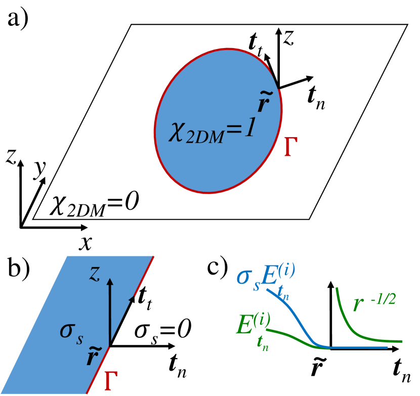
To find the correct factorization rule for Eq. (26), the continuity property of the two factors in the r.h.s. of this equation as well as that of the product have to be investigated. To this end, consider Fig. 6, which depicts the plane that comprises a surface conductivity, . Hereby, denotes the characteristic function of the 2DM distribution and is the sheet conductance of the 2DM, e.g. Eq. (2) for graphene. At each point, , of the 1D boundary of the 2DM we introduce a local coordinate system defined by the orthogonal vectors , , and , where and are the in-plane unit vectors normal and tangent to the contour , respectively, at the point and is the unit vector along the -axis. One can assume that the sheet conductance function is smooth along the direction, yet it is discontinuous along the direction, as per Fig. 6(b). The continuity relation, Eq. (25a), of the tangential electric field at allows one to define a tangential surface electric field, , as the limit of the volumetric electric fields, , from either side of plane:
| (27) |
The electromagnetic near-field in the vicinity of such a conductive sheet can be calculated analytically [76] and here we only summarize the main results relevant to our numerical method: i) The -component of the surface current vanishes at as
Since for , is continuous around . ii) The -component of the surface electric field, , is discontinuous at the boundary . More specifically,
that is inside the 2DM vanishes near the boundary, whereas it diverges when approaching the interface from outside the 2DM,
Finally, iii) the in-plane tangential component of the interfacial electric field is continuous and bounded at the boundary . Findings i) and ii) are schematically depicted in Fig. 6(c).
These results imply that is a continuous function but both factors, and , in Eq. (26) are discontinuous. Therefore, Laurent’s product rule cannot be applied, as it would result in spurious field oscillations near the boundary and slow convergence of the algorithm. The inverse rule is also not applicable, as the first factor, , vanishes in some regions of the unit cell, outside of the domains occupied by the 2DM. To overcome this problem, a small but nonzero surface conductivity, , is added at the interface regions where there is no 2DM with finite conductivity. As a result, this modified sheet conductance distribution in the unit cell is defined as:
| (28) |
As it has been seen in Section III.1, is a function of frequency and can vary by orders of magnitude. Therefore, it is natural to scale the added conductivity, , relative to the absolute value of the physical conductivity of the 2DM, that is , where is a small scaling constant. This choice ensures in addition that is a negative imaginary quantity, so that one does not introduce artificial losses in the system but only a vanishingly small phase change at the interface. However small this effect is, it introduces an error and hence its quantitative contribution to the optical response of the photonic structure must be investigated. The influence of , and implicitly that of , on the calculated near- and far-fields by the proposed method will be investigated in Section V.
A further justification of our nonzero conductivity model is provided by the application of Ampere’s law for a loop around the interface, an approach that has been recently introduced elsewhere [49, 55]. This alternative model also amounts to using a modified conductivity at the interface similar to that in Eq. (28).
In order to complete the derivation of the correct Fourier factorization of the surface current defined by Eq. (26) for , let denote a normal vector field (NVF), namely a vector field that is normal to the 1D contour at any point of the interface and is analytically continued into the regions away from . This can be done analytically for certain cross-sections and ways to automatically generate a NVF for arbitrary cross-sections are readily available [77]. This allows one to express the factorization of in terms of the conductivity distribution coefficients, and , and tangential field coefficients, , in such a way that the normal -component of is decomposed using the inverse rule, and its tangential -component is decomposed using the regular product rule:
| (29) |
where the conductivity difference matrix is given by
| (30) |
This procedure is similar to the factorization rule for the displacement field used in the regular RCWA for bulk materials employing the NVF approach for fast Fourier factorization given in (114); see also Refs. [73, 78].
The calculation of as a function of requires the electric near-field distribution at the interface. This near-field is difficult to calculate accurately in the RCWA even when the correct Fourier factorization rules are employed, as was noted in Refs. [56, 79, 78]. A revealing insight into the accuracy of near-field calculations is that RCWA relies on the accurate description of continuous quantities, as they can be readily expanded in Fourier series. This can be exploited to achieve an accurate interface-field description: knowing that the -component of the interface electric field, , is continuous, it is convenient to evaluate this component directly by Fourier series reconstruction. Since, however, its -component is discontinuous (and in fact singular), it can only be poorly represented by its Fourier series, so that the reconstructed field will experience unphysical oscillations and the Gibbs phenomenon.
A more well-behaved quantity is the surface current, which is continuous and hence properly described by its Fourier series. With the definition of the Fourier coefficients of the vectorial normal surface current and tangential surface fields as:
| (31a) | ||||
| (31b) | ||||
one obtains the reconstructed field at the interface as:
| (32) |
Here, all Fourier series represent functions continuous at the in-plane boundaries of the 2DM. The fact that this approach only allows a reconstruction of the near-field at the 2DM interface, where , is not particularly concerning since the nonlinear surface current is a priori nonvanishing there only.
IV.4 Inhomogeneous -matrix formalism
In he previous section we have introduced the modal expansion of the electromagnetic fields inside and around the diffraction grating structure and cast them in a concise matrix form, as per Eq. (24). It remains now to determine the coefficients in every computational layer in order to obtain the electromagnetic fields. This is achieved by fulfilling the boundary conditions given by Eq. (25b) between all computational layers, the results of these calculations being cast in a versatile inhomogeneous -matrix formalism.
To this end, let us consider again the multilayer structure and the computational variables defining the corresponding electromagnetic field schematically illustrated in Figs. 5(a) and 5(b), respectively. The optical structure consists of exactly one 2DM sheet located at , defined by its distribution of conductivity, and an arbitrary number of bulk layers, defined by their respective electrical permittivity distribution and identified by their superscript. Three of the layers are of particular interest, namely the two computational layers directly enclosing the 2DM sheet, identified by “” and “”, and the evaluation layer, “”, which can be any computational bulk layer in the grating structure. In addition, the semi-infinite layers “” and “” identify the cover and substrate, respectively. These capital letters are used to label the mode shape matrices, and , and the propagation matrix, , in each layer, . The vector of mode coefficients in each layer is denoted by the corresponding bold lower-case letters, , , , , and .
At each of the pump frequencies, plane wave incidence is assumed, i.e. the incoming cover and substrate coefficients, and , respectively, are given and at least one of their entries is nonzero. At the generated frequency, no field is assumed to be incident, hence . Moreover, the higher-harmonics optical field is generated due to the nonlinear surface current, . With this set-up, the goal of the remaining derivation is to determine the mode coefficients, , in the evaluation layer, . Since the layer was arbitrarily chosen, this suffices to determine the mode coefficients, and hence the electromagnetic field, in any layer.
Since the fields in layers and are expressed using their Fourier series according to Eq. (15), the boundary conditions given by Eq. (25) can be expressed in terms of the Fourier vector coefficients of the fields and read:
| (33a) | |||
| (33b) | |||
Hereby, denotes the variation of the tangential components of across the surface and the superscript, , is dropped to simplify the notation. The symbol “” means matrix transpose operation.
The vector Fourier coefficients, and , can be expressed in terms of their mode coefficients, and , via Eq. (24). This same procedure is performed with the linear surface current according to the factorization rule expressed by Eq. (29), which relies on the tangential field at . Due to the continuity of the tangential surface field, in principle, the field values from either side or , or their average, could be taken, as they are all equal. The latter is chosen in our approach, thus yielding .
Using the factorization rule given in Eq. (29), one obtains for the -component of the linear surface current:
| (38) | |||
| (43) |
Defining the block matrix for layers and as
| (46) |
the surface variation is found to be:
| (52) | ||||
| (58) |
Inserting this equation and Eq. (24) into Eqs. (33), the following matrix relation is derived:
| (65) |
where
Here, denotes the matrix of all tangential Fourier components of the modes in layer . Note that the vectors of Fourier coefficients have already been arranged in a way suitable for the -matrix formalism, which is explained in what follows.
By multiplying from the left both sides of Eq. (65) with the inverse of matrix , the Fourier coefficients of the outgoing modes, and , can be determined in terms of the coefficients of the incoming modes, and , and the nonlinear surface current:
| (72) | ||||
| (81) |
where is the scattering matrix (-matrix) of the interface system. This equation shows that the outgoing coefficients are comprised of two parts: and are the contributions to the total coefficients, and , respectively, given by linear scattering at the interface of the incident modes described by the coefficients and , whereas and are the contributions of the nonlinear surface current to the total coefficients and , respectively, and only enter if the generated frequency is considered.
If the considered structure only consists of cover, substrate, and one periodically patterned 2DM sheet, Eq. (72) is sufficient to fully describe its optical response. In multilayer structures, however, the contributions of -matrices of different layers and interfaces have to be properly incorporated. To this end, consider three layers, , , and , with coefficients , , and , respectively, depicted in Fig. 5(b). We assume that the -matrix, which connects the mode coefficients in layers and , is known and fulfills the relation
| (88) |
Combining this equation and Eq. (72), one determines the scattering matrix relation between the coefficients associated to the top and bottom layers, and , respectively, by eliminating the coefficients :
| (97) |
where the four sub-blocks of the combined -matrix, , are given by:
| (98a) | |||
| (98b) | |||
| (98c) | |||
| (98d) | |||
and the four sub-blocks of the combined matrix are expressed as:
| (99a) | |||
| (99b) | |||
| (99c) | |||
| (99d) | |||
These relations are found by straightforward matrix calculations, where one of the intermediate steps yields the coefficients of the middle layer, :
| (100a) | ||||
| (100b) | ||||
expressed solely in terms of incoming and known coefficients , and .
The matrix operation, , is known as the Redheffer star-product [80]. It is associative, noncommutative, and has the neutral element . It can be applied repeatedly and hence at all pump frequencies, where all nonlinear coefficients () vanish, it enables the calculation of the outgoing mode coefficients and from the incident mode coefficients, and .
Note that the term
| (107) |
in Eq. (97) can be viewed as the effective coefficients of the modes that are radiated by the combined multilayer-interface system, . More specifically, this term accounts for the linear propagation of the internally radiated modes at the generated frequency, with coefficients in bulk layer , and it accounts for linear optical interaction (reflection, transmission, and absorption) with the 2DM located at the -interface or the -layer-interface system.
Equipped with these matrix-vector relations, the calculation of all solution coefficients at the generated frequency can now be completed. In order to evaluate the mode coefficients in the evaluation layer , one calculates the combined -matrix, , of all layers and interfaces above the evaluation layer , and the combined -matrix, , of all interfaces and layers between the evaluation layer and up to but excluding the 2DM sheet. This is depicted in Fig. 5(c). Note that this procedure allows for , , or to be equal to , i.e. the evaluation layer can be any layer above the nonlinear 2DM sheet, which itself can be located at any interface, including just above the substrate.
Under these circumstances, the governing -matrix relations read as follows:
| (108e) | |||
| (108j) | |||
| (108q) | |||
By applying Eq. (97) to the matrix relations for and , one obtains and effective affine coefficients, and , as per Eq. (107).
The final constellation of the remaining two -matrices, and , and corresponding coefficients is depicted in Fig. 5(d). This configuration is similar to the initial system of -matrices, in Eq. (72) and in Eq. (88). Hence, it allows the calculation of the evaluation coefficients by means of Eq. (100), with the following replacements , , , , , , and , yielding
The treatment of an evaluation layer below the nonlinear layer can be performed in a similar manner. Moreover, if the structure contains more than one nonlinear 2DM sheet, the algorithm we just described can be repeated independently for each interface where nonlinear 2DM is located and then sum the individually obtained solution coefficients. It should be noted that in addition to the nonlinear optical response of 2DMs, the linear scattering effects at interfaces are naturally incorporated in our algorithm. This overall approach to linear and nonlinear light scattering in layered photonic structures containing 2DMs is possible because of the affine linearity of the total system.
V Validation of the numerical method and convergence analysis
In this section, aiming to validate our numerical method, we consider a series of generic test cases of diffraction gratings containing 2DMs and analyze the corresponding convergence characteristics of the numerical method. We consider both 1D- and 2D-periodic structures made of graphene, which has cubic nonlinearity. No additional test cases for the TMDC monolayers are shown here because they are far less challenging than graphene from a computational point of view: TMDC monolayers are poorly conductive materials and thus do not affect the optical field as strongly as graphene does.
In our analysis, we investigate physical quantities describing the near- and far-field, so as to fully assess the stability and convergence properties of our modal method, as was discussed in Ref. [78]. To characterize the far-field, we used the optical absorption, , at the FF, which is given by , where and denote the fraction of the intensity of the incident light that is reflected and transmitted, respectively. At the TH, the total radiation, , is chosen as a far-field quantity suitable to validate our method, where and denote the intensity at the TH radiated in the direction of reflection and transmission, respectively.
V.1 One-dimensional binary graphene gratings
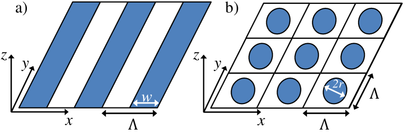
As a first example of a periodic diffraction grating containing nonlinear 2DMs, consider the 1D periodic array of graphene ribbons depicted in Fig. 7(a), sandwiched in-between homogeneous cover and substrate materials with electric permittivity, and , respectively. The period of the grating is and the spacing between adjacent ribbons is . The incident light is normally impinging onto this binary graphene grating and is TM-polarized.
In order to illustrate the effectiveness and benefits of our algorithm with added conductivity, Eq. (28) with , and correct Fourier factorization, Eq. (29), we compare it with two other versions of the proposed method. The first of these two algorithms employs a zero conductivity, , in the regions without graphene and only uses the product factorization rule for Eq. (26), i.e. an incorrect factorization rule. In the second algorithm we assume that graphene has a finite thickness, , i.e. we model the array of graphene ribbons as a periodic bulk layer with relative permittivity, . This can be done using a standard RCWA implementation. We stress, however, that this is computationally more costly as it involves the determination of the RCWA modes in this bulk layer representing the array of graphene ribbons. In addition, for the sake of completeness, computational results from Ref. [49] are included, too.
The linear absorption spectra calculated using a moderate number of harmonics, , are shown in Fig. 8(a). The device absorption presents a broad resonance peak with maximum of about at the wavelength, , with negligible absorption being observed at both shorter and longer wavelengths. The results obtained using the algorithm with added conductivity with shows very good agreement with those found using conventional bulk RCWA calculations and with the results taken from Ref. [49]. The model without added conductivity slightly overestimates the absorption, in the region .
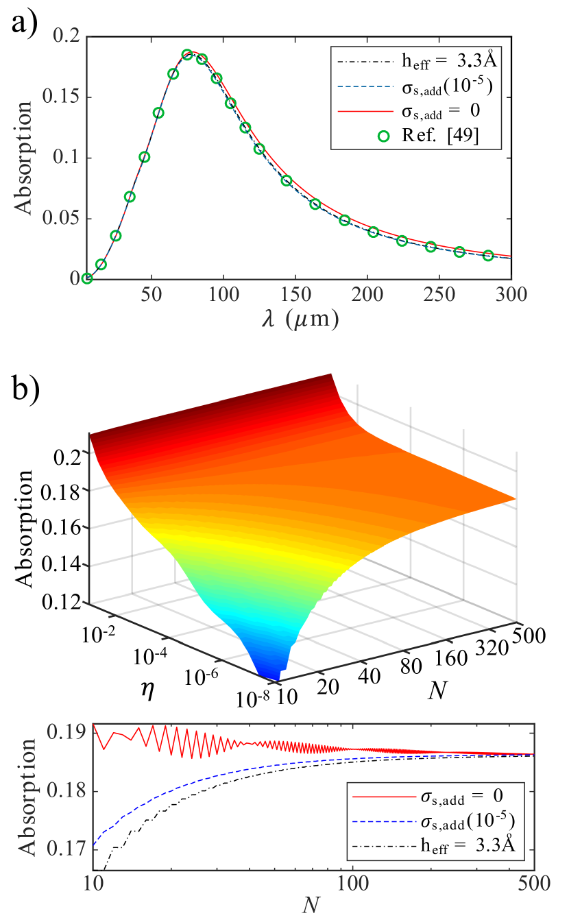
Keeping in mind that the sheet conductance of graphene, , has been introduced somewhat artificially to facilitate the use of the correct (inverse) factorization rule, the influence of on the accuracy of the computed results needs to be carefully investigated. The asymptotic behavior of both near- and far-field physical quantities are suitable tools for performing this analysis. To this end, we have determined the dependence of the absorption at on and , as depicted in Fig. 8(b). Among other things, this figure shows that the convergence with respect to is faster for larger . This dependence is not surprising, because the interface containing the structured graphene sheet becomes more optically homogeneous as increases, i.e. the description of as a Fourier series becomes more accurate. However, this does not prove the accuracy of the method just yet: was introduced at a purely mathematical level and as such it should vanish in physical diffraction gratings. The accuracy of the method is demonstrated by the fact that as , convergence of the absorption is reached; for example, as the maximum absorption converges to for increasing value of .
In the bottom panel of Fig. 8(b) we contrast the convergence characteristics of the three algorithms we just described. As it can be seen in this figure, all three approaches converge to the same value but, importantly, the convergence speed in the case of finite added conductivity is the fastest among the three cases. It is also instructive to remark that the slowest convergence is observed in the case of zero conductivity, an added drawback in this case being the oscillatory dependence of the absorption on , which confirms that this formulation is incorrect as was theoretically argued in Section IV.3.
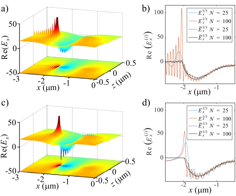
The spatial profile of the electric near-field deserves special attention as well because it reveals new important features pertaining to the convergence of the numerical method. To illustrate this idea, the -component of the electric field for the cases in which and when the conductivity is finite, , are shown in Figs. 9(a) and 9(c), respectively. The operating wavelength is and in both cases. In these plots, the boundary of the graphene ribbon in the unit cell is located at . It can be seen from these plots that without the added conductivity the field exhibits very strong, unphysical oscillations near the boundary of the graphene ribbons, i.e. at , which spread over the whole unit cell along the -direction. The spatial frequency of these oscillations is equal to the highest spatial discretization frequency, namely to . In the case of finite , on the other hand, there are no such spurious field oscillations outside graphene regions and only weak oscillations are seen inside the graphene ribbon, as per Fig. 9(c). In both cases, these field oscillations only occur very close to the interface where the graphene sheet is located and can merely be observed at distances . These oscillations are due to the fact that the Fourier series decomposition does not resolve the singularity of the electric field at the edges of the graphene ribbons, as we discussed in Section IV.3.
One of the aims of the accurate near-field formulation introduced by Eqs. (31) is to overcome this shortcoming of Fourier series decompositions and thus to allow the accurate field evaluation exactly at the location of the 2DM monolayers, i.e. at . To illustrate how our method achieves this, we depict in Figs. 9(b) and 9(d) the interface field, , for the cases in which and when the conductivity is finite, , respectively. Without using an added conductivity, the improper field evaluation of the surface field leads to a strongly oscillatory spatial dependence, which in addition changes significantly with , as shown by the blue and red lines in Fig. 9(b) for and , respectively. By contrast, the interface field obtained by using Eqs. (31) with replaced by displays hardly any oscillations, as per the black lines in this figure, yet it does not vanish at the edge of the graphene ribbon as required by the theoretical analysis presented in Section IV.3. These remaining oscillations are merely due to the fact that the incorrect factorization rule was used and not because of the unresolved singularity of the field.
This description changes significantly if one uses a small, finite value for , see Fig. 9(d). The improper evaluation using a finite value for yields a smooth field outside the graphene region, , but still displays unphysical oscillations inside the graphene region, , and does not vanish at the graphene boundary, , as required. On the other hand, by employing the correct evaluation of the surface field and surface current given by Eqs. (31), one obtains a surface field that vanishes at , is free of spurious oscillations, and converges rapidly with .
We stress that since the nonlinear polarization generated in our photonic structures is determined by the optical near-field at the location of 2DMs, an accurate evaluation of these near-fields is a paramount prerequisite to a rigorous description of the nonlinear optical response of these nonlinear photonic devices. To this end, as we just showed, this can be readily achieved by using the correct Fourier factorization expressed as Eq. (29) in the model with finite sheet conductance, the correct field evaluation given by Eqs. (31), and a properly chosen number of harmonics.
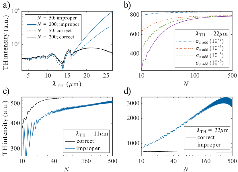
The total intensity of radiated TH is considered as the first quantity characterizing the nonlinear optical response of our graphene gratings, the corresponding computational results being summarized in Fig. 10. Thus, Fig. 10(a) depicts the total radiated power at the TH, determined for the case of finite added conductivity, , and number of harmonics, and . The nonlinear source current given by Eq. (6) was calculated using both the improperly evaluated interface field, , and the correctly calculated interface field, . Interestingly, in the wavelength range , both calculation methods yield qualitatively similar spectra. For longer wavelengths, however, results differ considerably and in fact only the results obtained using field converge.
Before investigating in more detail this behavior, we consider first the convergence characteristics of the far-field at the TH with respect to the value of the added conductivity, . The main features of this dependence, illustrated by the data plotted in Fig. 10(b), which corresponds to , are similar to those observed in the case of linear calculations. More specifically, the larger is the faster self-convergence with respect to is observed and the computational results converge for vanishingly small .
The difference in convergence behavior for increasing of the two approaches used to evaluate the surface field is illustrated in Figs. 10(c) and 10(d), for two representative wavelengths, and , respectively. These figures show that the correct field evaluation leads to rapid convergence at both wavelengths, whereas the improper approach yields slow and oscillatory convergence at and completely fails to converge at .
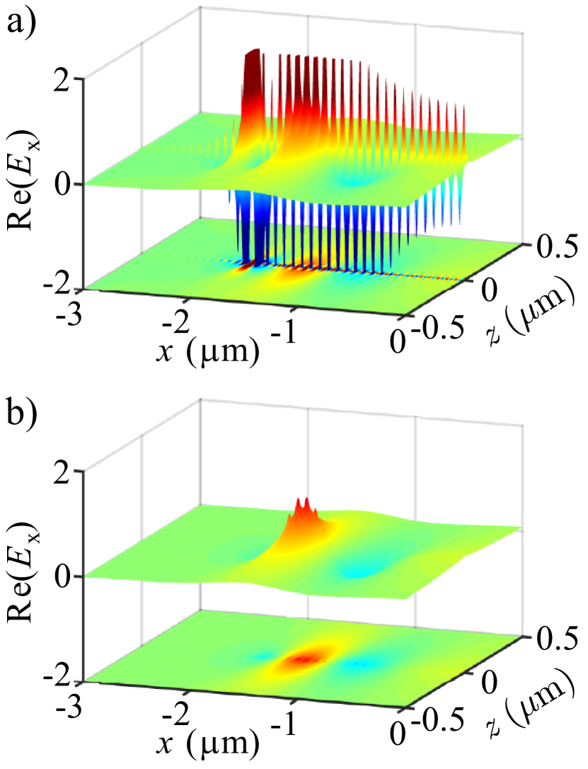
The electromagnetic near-field, , at the TH wavelength, , determined using the two algorithmic choices and spatial harmonics, is plotted in Fig. 11. Thus, the TH field derived from the nonlinear source polarization, , comprising the incorrectly evaluated field at the FF, , is completely swamped by unphysical oscillations, i.e. numerical artefacts, at the interface where the graphene ribbon is located, as per Fig. 11(a). On the other hand, the -component of the TH electric field, , which has the nonlinear polarization as its source, shows almost no oscillatory behavior and thus has the expected spatial profile, as shown in Fig. 11(b). Only further away from the interface, some agreement between the data in Figs. 11(a) and 11(b) can be observed.
The faster convergence, the more physically correct near-fields at both FF and TH, combined with the expected electric field behavior at graphene boundaries allow us to conclude that the properly evaluated field, , at the FF yields the correct results at the TH, whereas the TH optical response obtained using the improperly evaluated field, , at the FF is plagued by numerical artefacts and unphysical behavior.
V.2 Two-dimensional graphene diffraction gratings
Let us now consider 2D diffraction gratings that contain 2DMs, namely the periodically arranged graphene disks depicted in Fig. 7(b). We assume that the two periods are the same, and the diameter of the graphene disks is . For the sake of simplicity, we consider that the incoming light is normally impinging onto the grating, the cover and substrate media being air () and glass (), respectively.
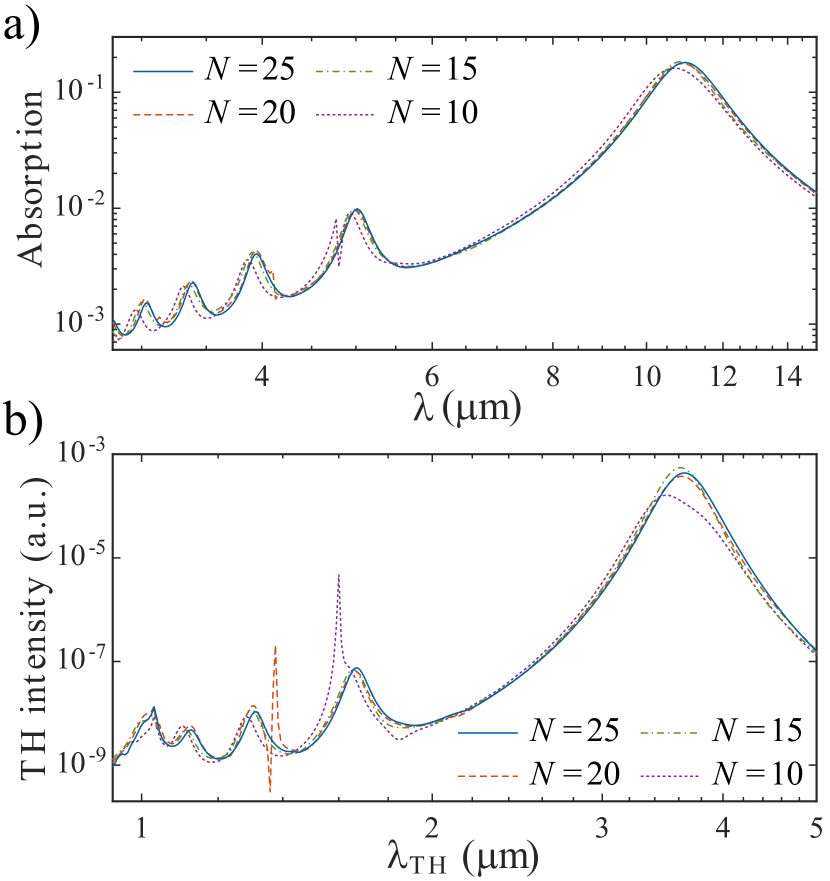
The absorption spectrum for -polarized incoming light, calculated for harmonics, is presented in Fig. 12(a). All results are obtained using the finite conductivity model defined by Eq. (28), the scaling parameter being . The zero-conductivity model or the improper interface field evaluation yield highly oscillatory near-field profiles at FF and TH and fails to deliver converging TH far-field results. Thus, it can be seen that the spectra calculated using different values of agree well and exhibit similar features. In particular, all spectra show a series of resonances whose amplitude and spectral width increase with the wavelength. Figure 12(b) depicts the dependence of the intensity of the total radiated TH from the array of graphene disks, , on the number of harmonics, . The nonlinear radiation spectra corresponding to the largest values and already show good agreement, which suggests that convergence has been achieved.
We now investigate in more detail the self-convergence characteristics of linear calculations, the main conclusions of this analysis being summarized in Fig. 13(a). We considered the wavelengths of the first three absorption resonances seen in Fig. 12(a), that is , , and . Setting as converged values the results obtained by using a large number of harmonics, , specifically , the relative self-error corresponding to a number of harmonics, , is then defined as:
| (109) |
This self-error function can be used as a reliable measure of the convergence of the method as long as the value of for which the reference absorption is defined is chosen to be sufficiently large.
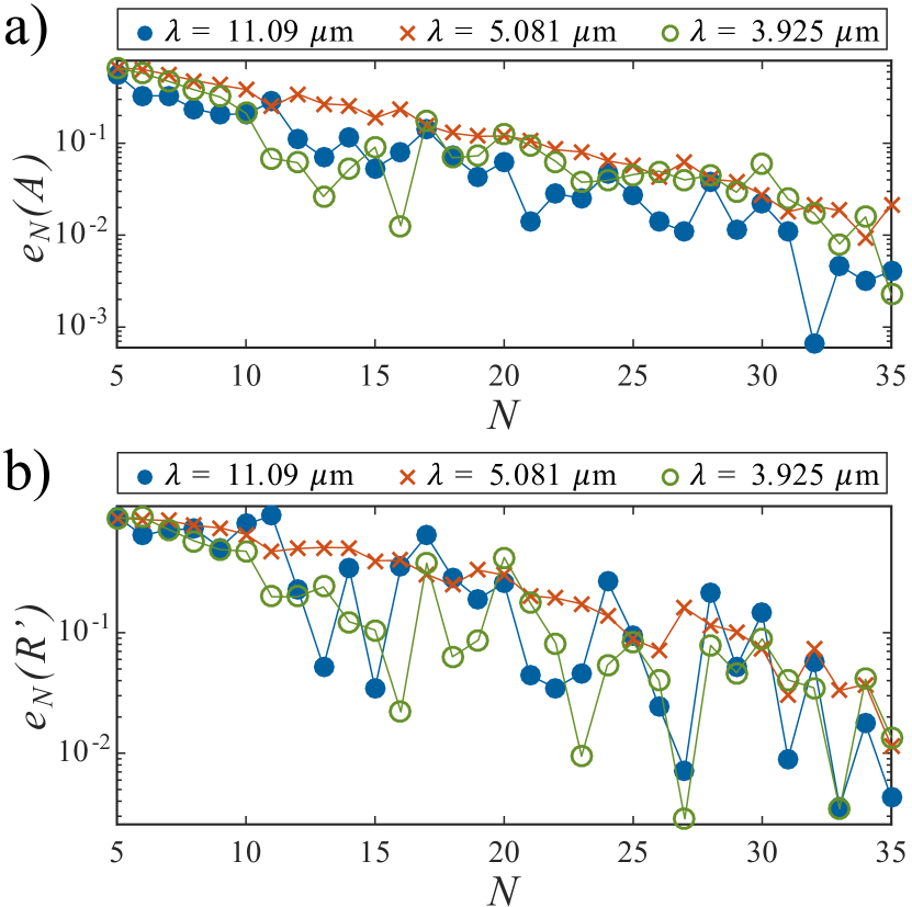
At all three resonance wavelengths, relative errors of are achieved for . It should be noted that in terms of computational effort, using in 2D simulations is comparable to using in 1D simulations. Moreover, the accuracy of the 2D simulation with is still correlated to and limited by the highest spatial frequency, .
To asses the convergence of the TH simulations more rigorously, the relative error, , of the TH radiation intensity, , for a given number of harmonics , which is defined similarly to in Eq. (109) with , is depicted in Fig. 13(b). A relative self error of can be achieved at for all three resonance wavelengths. Note also that the intensity of the TH radiation varies over six orders of magnitude and has maxima at the locations of the spectral resonances of the linear absorption, as per Fig. 12(a).
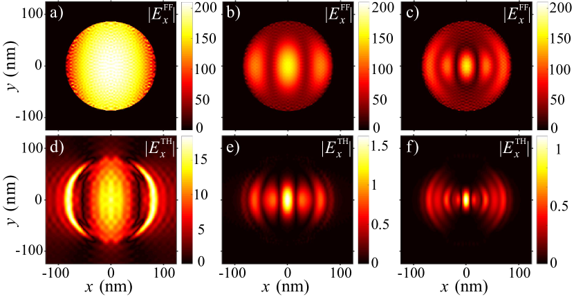
Graphene is a lossy conductor in the spectral range considered and therefore allows the excitation of surface waves [62, 47, 45]. This is the case with each of the absorption maxima seen in the linear spectrum, as illustrated by Figs. 14(a)–14(c). Thus, we show in these figures the dominant field component, , of the linear electric field at the first three resonance wavelengths, in Fig. 14(a), in Fig. 14(b), and in Fig. 14(c). These field profiles exhibit distinct mode shapes with one, three and five maxima, which demonstrates that the corresponding resonances represent the first three plasmon modes of the graphene disks.
Strongly enhanced and largely confined optical field resulting from the excitation of localized plasmon modes gives rise to enhanced THG. This fact is supported by the field profiles plotted in the bottom panels of Fig. 14, where the dominant electric field component at the TH, , is shown. Indeed, regions of strong field enhancement can be seen, with field profiles with three, seven, and eleven maxima being observed at in Fig. 14(d), in Fig. 14(e), and in Fig. 14(f), respectively.
VI Diffraction in nonlinear gratings containing 2D materials
In this section the linear and nonlinear optical response of diffraction gratings incorporating TMDC monolayer materials or graphene is investigated and the application of the inhomogeneous -matrix formulation introduced in Section IV.4 is illustrated in several specific cases.
Throughout this section, the intensity of the incident beam is chosen to be , which is a moderately high peak intensity generated by a pulsed laser. Changing the incident intensity in the undepleted pump approximation does not alter the numerical results at any of the incident frequencies, but it substantially changes the magnitude of the electromagnetic field at the generated frequency, . More specifically, for SHG and THG the intensity of the generated waves behaves as and , respectively, and as such they can increase to significant values. A problem that might arise in the undepleted pump approximation is that if the intensity of the generated waves becomes comparable to the intensity of the incident wave, the use of this approximation would become questionable. This is not the case in most practical situations and certainly not the case here, as can be seen by the intensity of generated optical fields in the examples hereafter.
VI.1 SHG from TMDC monolayer ribbons
To begin with, we consider a 1D binary TMDC grating placed on top of a glass substrate with . Its period is and the filling factor is . An -polarized plane wave is normally incident onto the grating and a spectral range of for the incident wavelength is considered. The computations were performed using harmonics and an added sheet conductance of , the results being presented in Fig. 15. The convergence of these calculations has been assured as diligently as for the binary graphene diffraction gratings discussed in Section V.1.
The plots presented in Fig. 15(a) reveal that the linear absorption spectra are primarily determined by the linear material properties of the TMDC materials. The absence of any additional resonant features in the spectra has two main reasons: the dielectric nature of the TMDCs does not allow the formation of plasmons, as in the case of graphene, whereas the vanishingly small thickness of the TMDC monolayers precludes the existence of geometric, Mie-type resonances. These explanations are supported also by the fact that linear and nonlinear spectra are qualitatively similar if one varies the grating period and the feature size of the TMDC ribbons.
In order to obtain the SH radiation of the 2DM grating, we used the nonlinear conductivity, , discussed in Section III.2. Since no values of for were available, we determined the nonlinear optical response of the grating only in the case of three TMDC materials, , , and . As our calculations showed that there is no resonant field enhancement at the TMDC ribbons at the FF, no strong enhancement of generated SH is expected. The nonlinear SH radiation spectra presented in Fig. 15(b) suggest that indeed the intensity of radiated SH closely follows the magnitude of , as can be found by comparison with the plots in Fig. 4(b). The maximal intensity of generated SH is , rendering valid the undepleted pump approximation.
VI.2 Nonlinear efficiency enhancement for TMDC monolayers on a slab waveguide
Since TMDC monolayers themselves do not possess optical modes, we use a different approach to achieve enhanced nonlinear optical interactions in these 2D materials. Thus, we combine a TMDC monolayer with a bulk structure that possesses waveguide modes whose excitation leads to strong local field enhancement. A very effective structure for this purpose is a periodically patterned slab waveguide, covered by a TMDC monolayer, as depicted in Fig. 16(a). Dielectric slab waveguides exhibit very narrow spectral resonances, due to the resonant excitation of guiding slab modes, a phenomenon that can be used to enhance linear and nonlinear optical response of certain devices [81, 82, 71, 83].
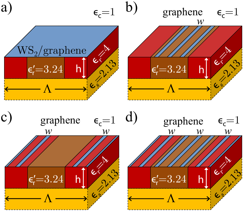
The waveguide structure under consideration consists of a slab of height, , placed between a monolayer WS2 and substrate with relative permittivity (index of refraction, ). The 2DM monolayer is adjacent to the cover region, which is assumed to be air, . The slab itself is periodically patterned, that is it consists of alternating regions with permittivity () and () with a period . This particular choice of parameters was inspired by Ref. [81].
For now, consider the unperturbed waveguide consisting of a material with relative permittivity . A slab waveguide supports optical guided modes and their excitation strongly affects its reflective and transmissive characteristics. A mode of order with in-plane propagation constant can be excited, when the in-plane wavenumber, , of an incident wave coincides with . This is not possible for a homogeneous waveguide due to the particular dispersion properties of and , but can be achieved if the waveguide permittivity is periodically modulated, as illustrated in Fig. 16(a). This periodic perturbation effectively folds the propagation constant into the first Brillouin-zone of the -space of the modes of the periodic waveguide and enables phase matching between and , i.e. the excitation of the mode . It should be stressed that, albeit less effectively, free-space photons couple to waveguide modes even if the periodic slab waveguide is covered by a thin, optically homogeneous layer, such as a 2DM, because the effective refractive index of the combined structure is periodic in this case, too.
In what follows, we demonstrate the resonant excitation of modes in the TMDC-waveguide structure for a fixed height of . Subsequently we optimize the height of the slab waveguide to obtain maximal generated SH and investigate the interplay between various resonant mechanisms in the combined waveguide-2DM device that lead to enhanced nonlinear optical response. Only monolayer WS2 is considered as covering 2DM in this example, because for this TMDC monolayer the dispersion of the nonlinear conductivity, , is known over the broadest spectral domain. The WS2 monolayer is oriented such that the arm-chair direction of the atomic lattice is aligned with the -axis of the structure. Due to the particular tensorial structure of , this configuration only yields TM-polarized SH for a TM-polarized fundamental field.
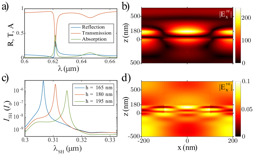
In order to illustrate the excitation of a waveguide mode, we considered a TM-polarized, normally incident plane wave in a wavelength range at FF of . The corresponding reflection, transmission, and absorption spectra are depicted in Fig. 17(a). A steep increase of the absorption is observed, from less than to a maximum of at . Moreover, the transmission and reflection have their minimum and maximum at this wavelength, respectively. This is due to the excitation of the TM0 waveguide mode, as can be confirmed by the inspection of the electric near-field profile in Fig. 17(b): has maxima at the top and bottom facets of the waveguide, which also implies a maximum of at its center, as one expects for a TM0 waveguide mode. Another local maximum of the absorption can be seen at and is due to one of the exciton absorption peaks of monolayer WS2 [c.f. Fig. 2(b)].
The enhancement of the fundamental field at the top of the waveguide, where the WS2 monolayer is located, yields a strongly increased intensity of SH radiation with a maximal value of , as shown in Fig. 17(c). Comparison of the radiation spectra for different waveguide heights, , , and , already shows the large sensitivity of the spectral location of waveguide modes to changing height. This is the basis for the parameter study in the remainder of this section. Before that, let us inspect the electric near-field at the SH wavelength, , presented in Fig. 17(d). This profile is markedly different from that of the linear near-field, namely it is spatially more inhomogeneous and has a different distribution of local minima and maxima. Finally, we point out that the absorption peak at does no translate to a notable increase of SH radiation, which is similar to the findings reported in Section VI.1.
In the rest of this section we explore the interplay among different resonant mechanisms in the combined waveguide-2DM structure that lead to enhanced nonlinear optical response and investigate how one can exploit them to increase the intensity of SH generated from this optical device. To this end, TM-polarized incident light in a wavelength range at the FF of is considered and simulations for waveguide height ranging from , using harmonics, are performed. The results of these calculations, corresponding to the FF, are shown in Fig. 18(a) in terms of the reflection spectra maps, and will be discussed now. The nonlinear part of the device study is summarized in Fig. 18(b) in terms of maps of its outgoing radiation at the SH and will be investigated subsequently.
The linear optical characteristics of the TMDC-covered waveguide determined for different heights are depicted as a 2D map of reflectivity values. This 2D map of reflection spectra exhibits a smooth dependence on and with minimal and maximal values of and , respectively, except when one of several mechanisms leads to resonant enhancement of the reflectivity. i) The most evident and spectrally broadest features are due to the Fabry-Perot interference mechanism, which yields maximal (minimal) reflectivity if the multiple reflections inside the slab waveguide are in (out-of) phase [84]. These Fabry-Perot resonances appear in the reflectivity map as spectrally broad variations from reflection minima to maxima. ii) The second kind of spectral feature is due to the resonant increase of intrinsic optical absorption of WS2, which occurs at wavelengths at which excitons are generated in the WS2 monolayer. The strongest of these absorption peaks is at . Their spectral location is determined by the dispersion of , given in Fig. 2(b), and is largely independent of the electromagnetic environment and hence does not depend on . The intrinsic optical absorption mostly increases the absorption in the combined waveguide-2DM device, but also leads to increasing reflection and decreasing transmission, as was already shown for around in Fig. 17(a). iii) The third kind of resonance is due to the excitation of TMν waveguide modes and manifests itself as a spectrally narrow, asymmetric, and steep variation of the reflectivity of the device. A detailed analysis of the resonant excitation of the TM0 mode for and was already presented in relation to Fig. 17. By varying the waveguide height and wavelength, the excitation of the TM1 and TM2 modes was found, too.
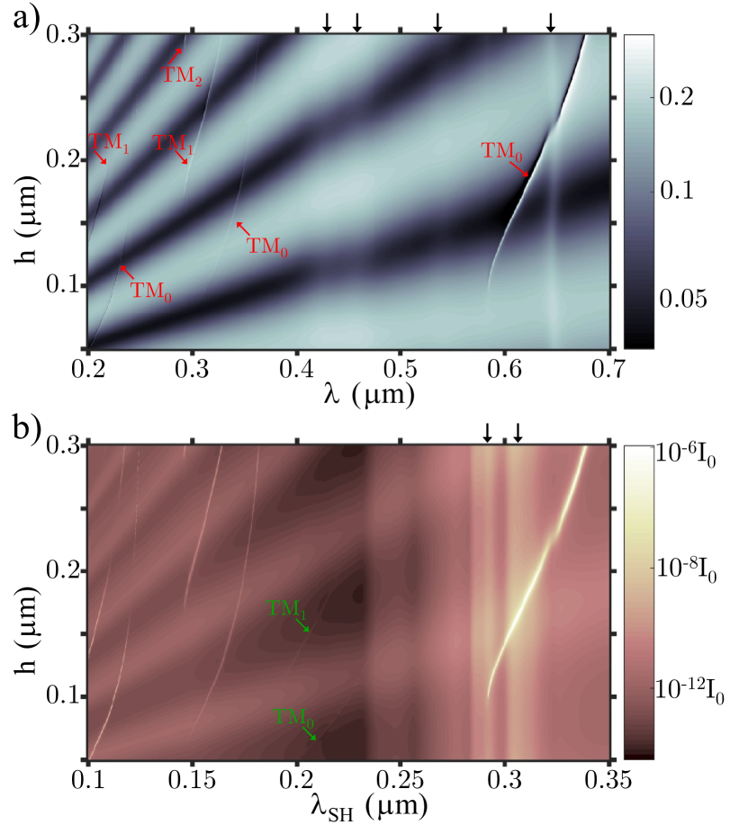
As the map in Fig. 18(a) suggests, there is a mutual interaction among resonances of the TMDC-covered waveguide, giving rise to several interesting phenomena. First, one can observe the generation of Fano resonances, which generally result from the interference between a discrete state and a broad continuum and are characterized by an asymmetric spectral profile [85, 86, 87]. Fano resonances arise via different scenarios in the considered structure, most notably due to the interference of the TM0 waveguide mode (the discrete state) and the Fabry-Perot resonance (the broad continuum). For example, for a device height of and for increasing wavelengths around , the reflection decreases to a minimum value of , then steeply increases to , as shown in Fig. 17(a). Similar behavior can be observed when TM1 and TM2 waveguide modes are excited. The absorption and transmission spectra exhibit similar features, but the spectral asymmetry, a characteristic feature of Fano resonances, is not as well pronounced in these cases. Hence, only the reflection is shown here. The second phenomenon revealed by Fig. 17(a) is the crossing of the TM0 waveguide mode with the spectrally highest exciton absorption peak of monolayer WS2. In particular, the two resonances exhibit an anti-crossing behavior at the wavelength of their strongest interaction, which is a well-known phenomenon in photonics and other physical systems [88, 89, 90].
Having understood the key features of the linear response of the combined waveguide-2DM optical system, we now explore its nonlinear optical properties. To this end, consider Fig. 18(b), which depicts the map of the intensity of the total generated SH at wavelengths, , ranging from and for the same values of the waveguide height as in Fig. 18(a). This intensity varies over almost 6 orders of magnitude, from a minimum of at and to a maximum of for and . It exhibits a smooth dependence on the system parameters, except for the excitation of certain resonances via mechanisms similar to those examined in the linear case.
In general, the nonlinear radiation is affected by two factors, which we call inherited and intrinsic effects. Inherited effects are due to the enhancement via certain mechanisms of the optical field at the FF, at the location of the WS2 monolayer, which increases the nonlinear source current and consequently the intensity of the generated SH. Intrinsic effects, on the other hand, are resonant effects at the SH wavelength, which can also influence the intensity of radiated waves at the SH.
The most important inherited effects leading to resonant enhancement of nonlinear radiation, seen in the map plotted in Fig. 18(b), are as follows: i) The inherited Fabry-Perot reflection minima lead to a moderate increase of the SH over broad wavelength ranges. ii) The excitation of waveguide modes at the FF leads to particularly strong enhancement of the fundamental field and yields the highest intensity of SH radiation, most notably when the TM0 mode is excited. In particular, SH radiation with intensity is consistently achieved when this mode is excited, except for fundamental wavelengths near the exciton absorption maximum at . iii) Finally, the interaction of the fundamental TM0 mode and the WS2 exciton leads to a reduced enhancement of the fundamental field, as compared to the case of the sole excitation of the TM0 mode, and results in a decrease of the SH intensity to .
Amongst the intrinsic effects, two important mechanisms that lead to enhancement of SH intensity were identified: i) The generated electric field at the SH wavelength acts as excitation waves for the TMDC monolayer-waveguide system and resonantly excites waveguide modes existing at the SH, namely the TM0 and TM1 modes. This leads to a relatively small increase in the SH intensity. ii) The frequency dispersion of the nonlinear optical conductivity of monolayer WS2 is apparent in the SH spectra: maxima of , which are naturally independent of the waveguide height, , correspond to maxima in the SH radiation spectrum. Moreover, the SHG due to the combined inherited TM0 mode and the intrinsic maximum of for three values of is presented in Fig. 17(c) and shows that the two effects constructively add to increase the intensity of the SHG.
Note that the reflection, transmission, and absorption spectra, the nonlinear radiation spectra, as well as the resonance wavelengths of the slab waveguide were accurately calculated even for the moderate number of harmonics, as was ensured with a convergence check for fixed height and with the rigorous procedures described in Section V.1. A total of simulations for pairs of were performed, where a higher spectral resolution was used near the resonance wavelengths of the device in order to accurately resolve the spectrally narrow effect of the waveguide resonances.
VI.3 Nonlinear interaction between waveguide modes and graphene plasmons
In the preceding section, we combined a 2D material, WS2, which does not support localized optical modes, with an optical device consisting of a periodic slab waveguide, and achieved a strong enhancement of the nonlinear efficiency of the combined device. In this section we follow a similar approach and combine a similar slab waveguide with graphene structures, which we have already shown that support localized surface plasmon modes, in order to achieve a multiresonant, highly nonlinear optical device. Thus, the structure under consideration is schematically depicted in Fig. 16(d). It consists of a periodically patterned slab waveguide with the same optical parameters as the one in the preceding section, which now is covered by graphene ribbons with width . We will call the three graphene ribbons centered on top of the material with permittivity and the inner and outer ribbons, respectively, which is natural given the definition of the unit cell in Fig. 16(d). The center-to-center distance of the inner ribbons (and outer ribbons) is and the center-to-center distance between a inner ribbon to a neighboring outer ribbon is . In this case, the height of the slab waveguide is and the period is .
The small feature size of the graphene ribbons, , is required to excite graphene plasmons at moderately small wavelengths, at which waveguide modes exist, too. This is not a conceptual drawback of this particular structure, but it is computationally costly to accurately resolve graphene ribbons with very small width. Thus, harmonics were used throughout this computational analysis and an added conductivity of was introduced.
To fully understand the linear and nonlinear optical properties of the graphene-waveguide structure, let us first investigate two less complex, complementary structures where the graphene ribbons are located on the waveguide sections with either low or high index of refraction, as per Figs. 16(b) and 16(c), respectively, and also the waveguide covered with an unstructured, uniform graphene sheet, as per Fig. 16(a).
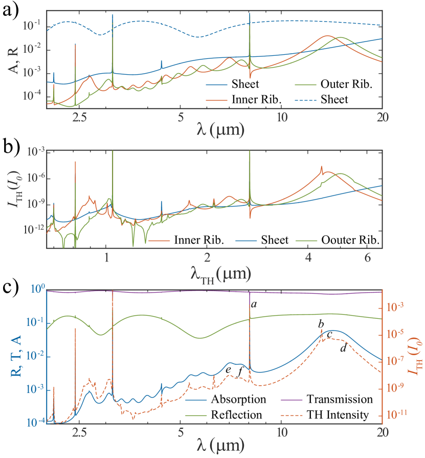
The linear absorption spectra for these three variations of the device, determined for values of the fundamental wavelength ranging from , are depicted in Fig. 19(a), where normal incidence and TM-polarization is assumed. The absorption of the waveguide with the covering graphene sheet follows a monotonously increasing trend, upon which alternating, broad local minima and maxima are superimposed. These maxima are due to the Fabry-Perot interference and primarily reveal themselves as maxima and minima of the device reflectivity, also shown in Fig. 19(a). The absorption spectra for the waveguide with graphene ribbons on top of the inner and outer parts of the waveguide exhibit relatively broad spectral peaks due to the excitation of surface plasmons in the graphene ribbons. Their excitation wavelength chiefly depends on the width of the ribbon and the permittivity of the underlying dielectric: the lower refractive index material () underneath the inner ribbons leads to excitation of plasmons at smaller wavelength than the wavelength corresponding to the plasmons in the outer ribbons, placed on top of waveguide sections with higher refractive index (). In all three devices, the absorption exhibits additional, spectrally narrow peaks with up to 30% absorption due to the excitation of optical modes in the slab waveguide grating.
The nonlinear radiation spectra in Fig. 19(b) complement these findings. Thus, the intensity of the TH radiation generated by the unstructured graphene sheet increases with wavelength and overlayed on it one can observe the effect of Fabry-Perot resonances. Moreover, the local field enhancement due to the excitation of localized surface plasmons in the inner and outer graphene ribbons leads to increased THG at lower and higher wavelengths, respectively. The inherited waveguide modes maximize the amount of generated TH radiation, which reaches values of up to .
The interplay of these resonant effects in the combined graphene-waveguide structure with ribbons distributed over the whole area of the waveguide is revealed by the results presented in Fig. 19(c). Note that the abscissa of this figure gives the values of the incoming wavelength, , for the linear reflection, transmission, and absorption spectra and the TH wavelength, , for the intensity of THG. The absorption at the FF displays an increasing trend in the range of ; however, there are several spectrally broad and narrow absorption peaks, which are the manifestation of different phenomena. Thus, the narrow resonances are due to the excitation of the TM0 mode of the slab waveguide, e.g. those at , , and . The electric field, , at the FF, , shows a strong enhancement at the top of the waveguide region, as per Fig. 20(a, top). Similarly to the TM0 mode shown in Fig. 17(b), this field profile has two maxima over the -extent of one unit cell of the grating and two maxima along the -extent of the waveguide, where the maximum near the top of the waveguide is much larger than the one at the bottom. This strong fundamental field enhancement increases the absorption to and leads to a strong nonlinear source current, which in turn generates a strong electric field at the TH, the near-field of which is depicted in Fig. 20(a, bottom). This TH field is mostly localized around the graphene ribbons and has an evanescent nature. The total intensity of TH radiated into the cover and substrate amounts to .
The excitation of the TM0 mode at is equally interesting. It appears both as a sharp local maximum in the linear absorption spectrum at and as an increase of TH intensity at the TH wavelength in Fig. 19(c). The nonlinear electric near-field profile in Fig. 20(b, bottom) confirms the excitation of this intrinsic nonlinear TM0 mode for .
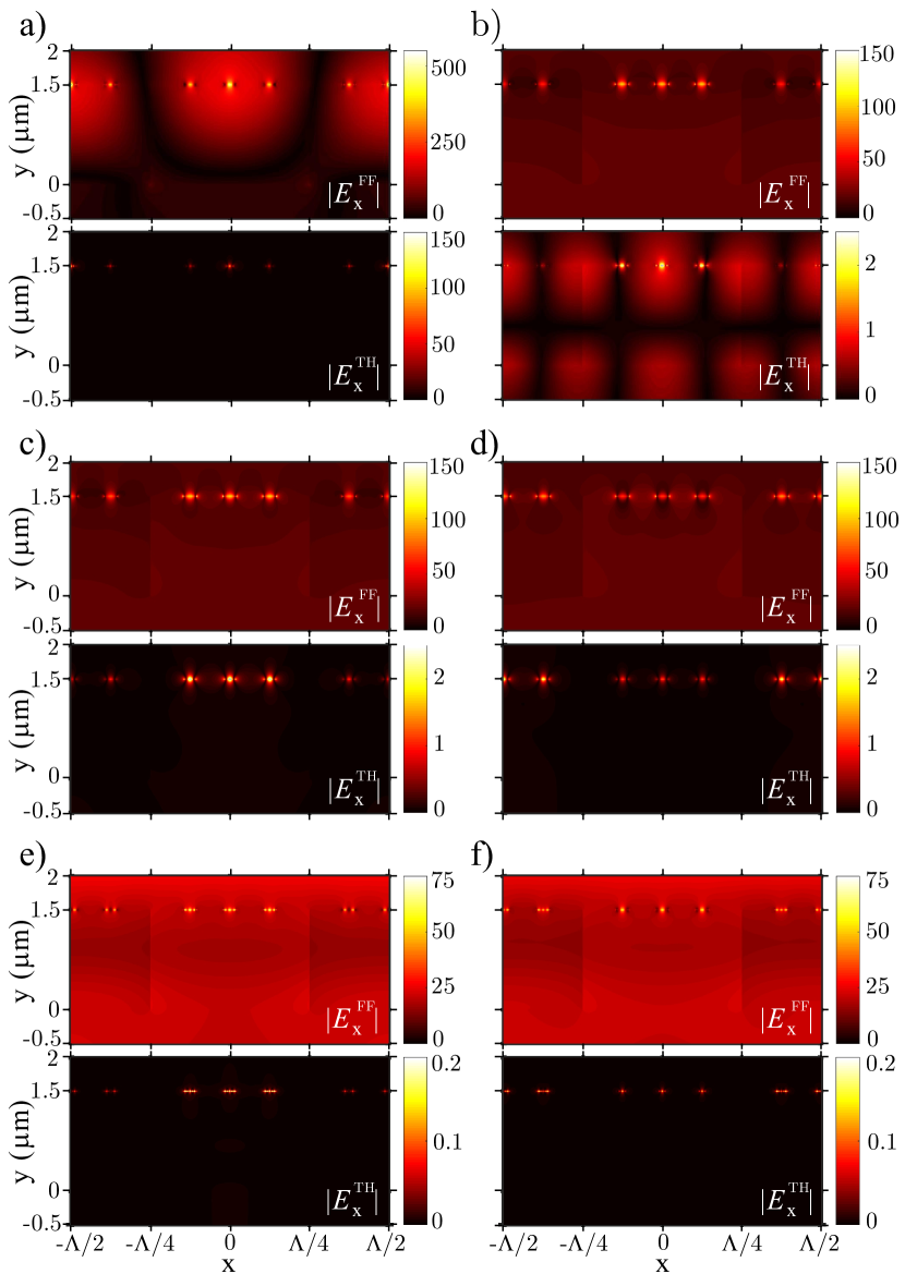
Another reason for increased absorption is the excitation of localized surface plasmons on the graphene ribbons. In order to illustrate this, let us consider the two absorption peaks with largest wavelengths, around and . The absorption maximum with the largest wavelength appears in the linear spectrum as a very broad resonance around , but the electric near-field profiles in the two top panels of Figs. 20(c) and 20(d) reveal that the actually surface plasmons are excited on the inner and outer graphene ribbons at slightly different wavelengths, and , respectively, which is explained by the difference in the electromagnetic environment probed by the corresponding plasmons. The excitation of these surface plasmons can also be seen in Fig. 19(c), as the local maxima labeled by “c” and “d”. Moreover, they can be viewed directly in the nonlinear far-field radiation spectrum, too, as spectrally separated peaks. As a consequence of excitation of localized surface plasmons, the TH near-field shows its highest values near the inner and outer ribbons at the TH wavelengths, and , as illustrated in the bottom panels of Figs. 20(c) and 20(d), respectively.
Similar physics describe the lower-order plasmon corresponding to . Thus, by inspecting the profiles of the fundamental near-field in the top panels of Figs. 20(e) and 20(f), one can see that, correspondingly, a plasmon with three peaks in the field profile is excited on the inner ribbons at whereas this same type of plasmon is excited on the outer ribbons at . This near-field pattern is in accordance to the surface plasmon field profiles that were found in Section V.2, Fig. 14(b). Moreover, no optical coupling between the plasmonic fields near adjacent ribbons could be observed. The spectra of the TH radiation at the wavelengths and also exhibits two local maxima, due to the enhancement of the fundamental field. The number of electric field maxima near the inner and outer graphene ribbons in the bottom of Figs. 20(e) and 20(f), respectively, agrees with the 5 field maxima in Fig. 14(d).
The two physical mechanisms that lead to the resonant enhancement of the optical response of the graphene-waveguide structure can partly be observed in the reflection and transmission spectra at the fundamental wavelength, which mainly exhibit a variation between minima and maxima due to the Fabry-Perot interference. This pattern is complemented by spectrally very narrow regions of increased reflection and decreased transmission due to the excitation of waveguide modes. The influence of surface plasmons on the reflection and transmission is only apparent at the largest excitation wavelengths around , where reflection and transmission are notably increased and decreased, respectively.
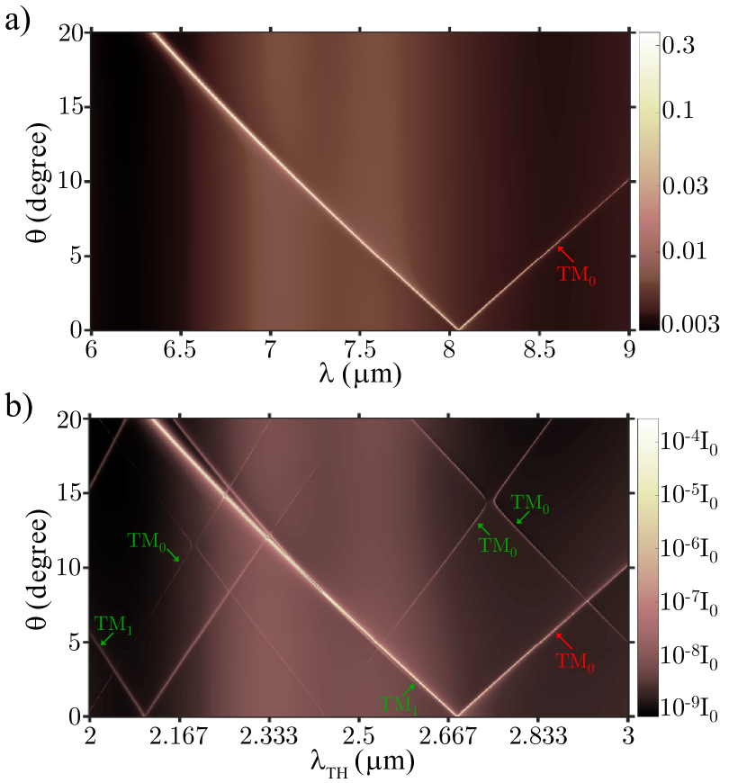
An effective way of tuning the characteristics of the light radiated by our nonlinear diffraction grating is by varying the angle of incidence of the incoming light. Not only will this showcase the effectiveness of the proposed numerical method in the oblique-incidence configuration, but it will also demonstrate the influence of the angle of incidence on the optical response of the grating. For example, the interaction of the spectrally narrow TM0 waveguide mode at with the two broad continua corresponding to the excitation of graphene plasmons at and provides a convenient optical setting for studying a tunable Fano resonance resulting from the interaction between a discrete state and multiple continua, a phenomenon that has recently been explored in a different plasmonic structure [91].
To investigate the interaction between a waveguide mode and the two absorption peaks, simulations with harmonics have been performed for increasing angle of incidence, , ranging from (and constant azimuthal angle ) in the fundamental wavelength range of the second-order plasmon peak, namely from . Higher spectral resolution was employed near the waveguide resonance wavelengths of the slab waveguide.
The resulting absorption map is shown in Fig. 21(a). The spectrum for is the same as in Fig. 19(c) and shows two broad maxima of , due to the excitation of surface plasmons, and a sharp maximum of due to the excitation of the TM0 waveguide mode at . Increasing the angle of incidence, , leaves the spectral location of the plasmon excitation unchanged; however, the spectral location of the waveguide mode resonance varies. For , the TM0 mode is excited at two wavelengths, and . Their separation from increases with and a more effective excitation on the left branch of the TM0 mode can be seen as compared to the right branch. For and the wavelengths of the mode, and , coincide with the central wavelength of the plasmon absorption peaks of the inner and outer ribbons, yielding absorption of and , respectively.
Along the TM0 band, i.e. the path of excitation of the TM0 mode in the ()-space, strong enhancement of conversion efficiency due to inherited effect of this mode can be observed in Fig. 21(b). The simultaneous excitation of waveguide modes and graphene plasmons yields strong THG, with intensities of at and and at and . However, the strongest TH intensity of is generated at and , namely where the intrinsic TM1 band crosses the inherited TM0 band. The increase of the conversion efficiency due to sole excitation of the intrinsic nonlinear modes is notable, but orders of magnitude lower than in the case of inherited effects, e.g. the same intrinsic TM1 mode away from the simultaneous resonance, at and , yields TH radiation of intensity .
Inspection of the bands of the intrinsic modes reveals and additional interesting feature. Specifically, intrinsic modes of the same order show anti-crossing behavior, e.g. TM0 at and or TM1 at and , whereas bands of different intrinsic modes pass through each other, i.e. TM0 and TM1 at and . This crossing of modes of same order occurs when the transverse component of the incident vector, , reaches the edge of the first Brillouin zone.
VII Concluding Remarks
In conclusion, we have derived an improved, an accurate formulation of the rigorous coupled-wave analysis (RCWA) method to describe linear and nonlinear optical interactions between light and periodically patterned 2D materials, such as graphene and transition-metal dichalcogenide (TMDC) monolayers. Unlike previous approaches, our numerical formalism does not depend on the height of the 2D material, a poorly defined physical quantity, and as such is applicable to any 2D material, as long as their linear and nonlinear optical surface conductivities are known. A key ingredient that markedly improves the accuracy and convergence of this numerical method is a vanishingly small, added conductivity, which allows for correctly solving the Fourier factorization problem and consequently a reliable computational investigation of 2D materials. In particular, this small value of the added conductivity yields accurate results when convergence with respect to the number of harmonics has been achieved. The proposed numerical method also allows one to describe the nonlinear optical response of generic periodically patterned 2D materials. In this context, we have found that correct nonlinear optical physics in these structures can only be captured when using the accurate near-field formulation of RCWA introduced in [78]. Importantly, our approach employing boundary conditions for the linear and nonlinear fields can be readily extended to other methods [92, 93, 94] used to describe nonlinear optical effects at interfaces, as in the case of graphene and TMDC monolayer materials the optical higher-harmonics are generated in a single atomic layer.
Our numerical method has been comprehensively validated by comparing its predictions to results obtained using an alternative method. Upon successful validation, we have used it to investigate the characteristics of various kinds of diffraction gratings comprising graphene and TMDC monolayers. We found that these materials interact differently with light, which is explained by their metallic or semiconductor nature. Thus, graphene exhibits THG as the lowest-order nonlinear optical interaction, due to the inversion symmetry properties of its atomic lattice, and supports surface plasmons. We found that the excitation of surface plasmons leads to increased linear absorption and enhanced THG, which points to significant potential for tunable THG in graphene. The TMDC monolayer materials, on the other hand, are semiconductors and non-centrosymmetric. As a result, their linear optical absorption spectra show a series of exciton resonances, whereas in this case the SHG is the lowest-order nonlinear optical process.
As an application of our numerical method, we have demonstrated that by coupling a TMDC monolayer with a photonic structure that possesses optical resonances, namely a periodically patterned slab waveguide, one can achieve strong, frequency selective field enhancement and consequently increased nonlinear optical response of the TMDC monolayer. In addition, we have showed that by coupling graphene with a similar waveguiding device, the interplay between plasmon resonances in graphene and leaky waveguide resonances of the slab waveguide leads to rich physics explained by intriguing phenomena, such as multi-continua Fano resonances and enhanced SHG via simultaneous excitation and efficient coupling of optical modes at the FF and SH.
The formulation of our method is general enough to describe most nonlinear optical processes of practical interest in the undepleted pump approximation, which is valid in essentially all experimental settings. In order to tackle those cases where this approximation might be less accurate, such as the optical Kerr effect, one can easily extend our method beyond the undepleted pump approximation by employing an iterative, self-consistent solution process, similar to the approach introduced in [95, 96, 97] for describing optical Kerr effects in periodic bulk media. Equally important, it is also possible to investigate important carriers related optical effects in 2D materials with the proposed method, namely the influence of charge doping on the optical properties of photonic structures containing 2D materials. Whereas a rigorous description of transient effects in such systems would require the incorporation of charge dynamics in our numerical algorithm, a nontrivial but tractable task, the optical response in the steady-state can be determined by simply modifying the electric permittivity of the 2D materials so as to take into account the dependence of the permittivity on the charge density.
Acknowledgements.
This work was supported by the European Research Council, Grant Agreement no. ERC-2014-CoG-648328. The work of M. W. was partly supported through a UCL Impact Award graduate studentship funded by UCL and Photon Design, Ltd. The authors thank Y. S. Kivshar and D. F. G. Gallagher for many insightful discussions and wish to acknowledge support from the Royal Society’s International Exchanges Scheme and the hospitality of the Nonlinear Physics Centre of the Australian National University. The authors acknowledge the use of the UCL Legion High Performance Computing Facility (Legion@UCL) and associated support services in the completion of this work.*
Appendix A Outline of the rigorous coupled-wave analysis
For the sake of completeness, we outline in this Appendix the mathematical description of the RCWA based approach used to find the layer-wise solution of the diffraction grating problem. For now, let us drop the superscript , as the description of the modal form of the electromagnetic field is independent on whether a pump or generated frequency is considered.
Known as the Bloch theorem, the solution of MEs for a periodic structure is pseudo-periodic, i.e. periodic with an additional transverse phase shift. Therefore, the permittivity of the structure in the -plane can be expressed as a 2D Fourier series:
| (110) |
with -dependent coefficients . The sum over is to be understood as the double infinite sum over the integers , . Similarly, the electromagnetic field quantities, , can be expressed as a Fourier series with phase shift,
| (111) |
where is the component of the th diffraction order. The intrinsic phase shift is determined by the transverse component of the -vector of the incident plane wave, . The sequence of Fourier coefficients shall be denoted by , and the evaluation of a Fourier by means of the sum in Eq. (111) is denoted by the reconstruction operator, .
In actual calculations, the infinite sums in Eqs. (110) and (111) have to be truncated. A rectangular truncation approach, namely , will be used throughout this derivation, yielding a total of Fourier series coefficients (or harmonics).
In the remaining part of the section we will provide the general mathematical formulation of the modal field expansion of the electromagnetic field. Thus, the underlying assumption of the modal field expansion in a periodic bulk layer of the grating is that the permittivity function, , in layer is -invariant, where and denote the bottom and the top of the periodic bulk layer. This implies that the Fourier coefficients, , of are -independent, too.
Since the field solution is periodic according to Bloch theorem, the electromagnetic fields inside this periodic bulk layer are pseudo-periodic, i.e. they can be expressed as Fourier series with phase shift using the reconstruction operator, :
| (112a) | ||||
| (112b) | ||||
Before using these ansatz functions to determine the electromagnetic fields, the correct Fourier factorization rules [75, 72, 54, 73] have to be used in order to factorize the product,
| (113) |
as they ensure accuracy and convergence of the RCWA modal expansion even for low number of harmonics.
In this work, the normal vector field approach [73, 78] in bulk layers is used to accurately solve the Fourier factorization problem in 2D. To this end, let be a continuation of the surface normal vectors of the grating structure, i.e. a normal vector field. The Fourier series factorization of the constitutive relation Eq. (113) then reads,
| (114) |
where is the Kronecker delta. Here, denotes the Toeplitz matrix of Fourier coefficients of a function , and the matrix is given by , with and being the -component of the normal vector field, , at the material boundary.
Inserting Eq. (112), the permittivity given by Eq. (110), and the correct factorization provided by Eq. (114) into the MEs one obtains a linear system of ordinary differential equations for the -dependent amplitudes of the modal fields. This system is solved assuming exponential dependency for modal Fourier coefficients, and , with the complex propagation constant, . Then, the system of ordinary differential equations can be rewritten as an algebraic eigenvalue problem for ,
| (119) |
and an additional relation for ,
| (124) |
In these relations, are matrices of block-matrix form:
Here, , the matrices , , are diagonal matrices of the in-plane propagation constants, , of the diffraction orders, and I is the identity matrix of size .
The eigenvalue problem defined by Eq. (119) has solutions consisting of the eigenvalues and eigenvectors , . Defining the positive and negative roots of as
respectively, one obtains a total of upward and downward propagating modes of the grating. The upward (downward) mode with index is defined by its propagation constant, (), and its transverse mode profile given by the Fourier vector coefficients, and ( and ), where () are obtained from Eq. (124) by setting ().
Since the bulk grating layer is considered to be made of linear optical materials, the linear superposition of modes is a solution to the MEs, too. Therefore, the total electric field in the grating is given by
| (125) |
where the complex mode coefficient () determines the contribution of each upward (downward) propagating mode to the total grating field and () denotes the -coordinate of the bottom (top) of the considered grating layer. The components of the magnetic field, , can be found from a similar equation. Given this structure of the modes, the electromagnetic fields in the grating are hence fully determined by mode coefficients, . Their values are obtained by means of the electromagnetic boundary conditions described in Section IV.4.
For reasons related to the practical implementation of RCWA, it is useful to rewrite Eq. (125) in terms of -dependent Fourier coefficients, similar to Eqs. (112), but interchanging the order of summation of modes and Fourier components in Eq. (125):
| (126a) | |||
| (126b) | |||
where and are given by:
| (127a) | ||||
| (127b) | ||||
Here, the mode-shape matrix () contains the vector of Fourier coefficients, (), in its th column. Moreover, the propagation matrix, , is a diagonal matrix containing the -dependence of each mode on its diagonal, , with , and denotes the vector of upward (“”) and downward (“”) propagating mode coefficients.
Using Eqs. (126) and (127) one can determine the electromagnetic field everywhere in and around the grating, namely in the periodic or homogeneous bulk layers forming the grating as well as in the cover and substrate. However, for homogeneous layers a Rayleigh expansion [72] with the diffraction orders as modes is preferable to the solution of the RCWA eigenproblem defined by Eq. (119) as it is computationally less demanding to calculate , , and for the Rayleigh expansion.
As a concluding remark, we note that the importance of Eqs. (127) resides in that it translates the electromagnetic field from its modal representation to its direct representation as Fourier series. The modal representation in terms of , , and in the r.h.s. of Eqs. (127) is restricted to a computational layer, but very advantageous therein, as it separates mode-shape quantities, , propagation and decay constants , and excitation strength coefficients . On the other hand, the direct field representation as a Fourier series with coefficients in the l.h.s. of Eqs. (127) has the same complex exponentials, , as basis functions everywhere in the grating, and hence it facilitates the comparison of quantities in different computational layers.
References
- Novoselov et al. [2004] K. S. Novoselov, A. K. Geim, S. Morozov, D. Jiang, Y. Zhang, S. Dubonos, I. Grigorieva, and A. Firsov, Science 306, 666 (2004).
- Novoselov et al. [2005a] K. Novoselov, A. K. Geim, S. Morozov, D. Jiang, M. Katsnelson, I. Grigorieva, S. Dubonos, and A. Firsov, Nature (London) 438, 197 (2005a).
- Novoselov et al. [2005b] K. S. Novoselov, D. Jiang, F. Schedin, T. J. Booth, V. V. Khotkevich, S. V. Morozov, and A. K. Geim, Proc. Natl. Acad. Sci. USA 102, 10451 (2005b).
- Lee et al. [2008] C. Lee, X. Wei, J. W. Kysar, and J. Hone, Science 321, 385 (2008).
- Frank et al. [2007] I. Frank, D. M. Tanenbaum, A. Van der Zande, and P. L. McEuen, J. Vac. Sci. Technol. B 25, 2558 (2007).
- Meyer et al. [2007] J. C. Meyer, A. K. Geim, M. Katsnelson, K. Novoselov, T. Booth, and S. Roth, Nature (London) 446, 60 (2007).
- Balandin et al. [2008] A. A. Balandin, S. Ghosh, W. Bao, I. Calizo, D. Teweldebrhan, F. Miao, and C. N. Lau, Nano Lett. 8, 902 (2008).
- Ghosh et al. [2008] S. Ghosh, I. Calizo, D. Teweldebrhan, E. Pokatilov, D. Nika, A. Balandin, W. Bao, F. Miao, and C. N. Lau, Appl. Phys. Lett. 92, 151911 (2008).
- Morozov et al. [2008] S. V. Morozov, K. S. Novoselov, M. I. Katsnelson, F. Schedin, D. Elias, J. A. Jaszczak, and A. K. Geim, Phys. Rev. Lett. 100, 016602 (2008).
- Lin et al. [2010] Y.-M. Lin, C. Dimitrakopoulos, K. A. Jenkins, D. B. Farmer, H.-Y. Chiu, A. Grill, and P. Avouris, Science 327, 662 (2010).
- Schwierz [2010] F. Schwierz, Nat. Nanotechnol. 5, 487 (2010).
- Xu et al. [2013] M. Xu, T. Liang, M. Shi, and H. Chen, Chem. Rev. 113, 3766 (2013).
- Song et al. [2010] L. Song, L. Ci, H. Lu, P. B. Sorokin, C. Jin, J. Ni, A. G. Kvashnin, D. G. Kvashnin, J. Lou, B. I. Yakobson, and P. M. Ajayan, Nano Lett. 10, 3209 (2010).
- Vogt et al. [2012] P. Vogt, P. De Padova, C. Quaresima, J. Avila, E. Frantzeskakis, M. C. Asensio, A. Resta, B. Ealet, and G. Le Lay, Phys. Rev. Lett. 108, 155501 (2012).
- Wang et al. [2012] Q. H. Wang, K. Kalantar-Zadeh, A. Kis, J. N. Coleman, and M. S. Strano, Nat. Nanotechnol. 7, 699 (2012).
- Nair et al. [2008] R. Nair, P. Blake, A. Grigorenko, K. Novoselov, T. Booth, T. Stauber, N. Peres, and A. Geim, Science 320, 1308 (2008).
- Bonaccorso et al. [2010] F. Bonaccorso, Z. Sun, T. Hasan, and A. Ferrari, Nat. Photon. 4, 611 (2010).
- Chen et al. [2012] J. Chen, M. Badioli, P. Alonso-Gonzalez, S. Thongrattanasiri, F. Huth, J. Osmond, M. Spasenovic, A. Centeno, A. Pesquera, P. Godignon, A. Zurutuza Elorza, N. Camara, F. J. G. de Abajo, R. Hillenbrand, and F. H. L. Koppens, Nature (London) 487, 77 (2012).
- Fei et al. [2012] Z. Fei, A. S. Rodin, G. O. Andreev, W. Bao, A. S. McLeod, M. Wagner, L. M. Zhang, Z. Zhao, M. Thiemens, G. Dominguez, M. M. Fogler, A. H. C. Neto, C. N. Lau, F. Keilmann, and D. N. Basov, Nature (London) 487, 82 (2012).
- Jablan et al. [2009] M. Jablan, H. Buljan, and M. Soljacic, Phys. Rev. B 80, 245435 (2009).
- Ju et al. [2011] L. Ju, B. Geng, J. Horng, C. Girit, M. Martin, Z. Hao, H. A. Bechtel, X. Liang, A. Zettl, Y. R. Shen, et al., Nat. Nanotechnol. 6, 630 (2011).
- Bao and Loh [2012] Q. Bao and K. P. Loh, ACS Nano 6, 3677 (2012).
- Jablan et al. [2013] M. Jablan, M. Soljacic, and H. Buljan, Proc. IEEE 101, 1689 (2013).
- Luo et al. [2013] X. Luo, T. Qiu, W. Lu, and Z. Ni, Mat. Sci. Eng. R 74, 351 (2013).
- Yeung et al. [2014] K. Y. Yeung, J. Chee, H. Yoon, Y. Song, J. Kong, and D. Ham, Nano Lett. 14, 2479 (2014).
- Smirnova et al. [2015a] D. A. Smirnova, A. E. Miroshnichenko, Y. S. Kivshar, and A. B. Khanikaev, Phys. Rev. B 92, 161406 (2015a).
- Smirnova et al. [2015b] D. A. Smirnova, R. E. Noskov, L. A. Smirnov, and Y. S. Kivshar, Phys. Rev. B 91, 075409 (2015b).
- Hong et al. [2013] S.-Y. Hong, J. I. Dadap, N. Petrone, P.-C. Yeh, J. Hone, and R. M. Osgood Jr, Phys. Rev. X 3, 021014 (2013).
- Cheng et al. [2014a] J. L. Cheng, N. Vermeulen, and J. E. Sipe, New J. Phys. 16, 053014 (2014a).
- Zhang et al. [2012] H. Zhang, S. Virally, Q. Bao, L. K. Ping, S. Massar, N. Godbout, and P. Kockaert, Opt. Lett. 37, 1856 (2012).
- Bykov et al. [2012] A. Y. Bykov, T. V. Murzina, M. G. Rybin, and E. D. Obraztsova, Phys. Rev. B 85, 121413 (2012).
- Cheng et al. [2014b] J. Cheng, N. Vermeulen, and J. Sipe, Opt. Express 22, 15868 (2014b).
- An et al. [2014] Y. Q. An, J. E. Rowe, D. B. Dougherty, J. U. Lee, and A. C. Diebold, Phys. Rev. B 89, 115310 (2014).
- Xia et al. [2009] F. Xia, T. Mueller, Y. Lin, A. Valdes-Garcia, and P. Avouris, Nat. Nanotechnol. 4, 839 (2009).
- Radisavljevic et al. [2011] B. Radisavljevic, A. Radenovic, J. Brivio, V. Giacometti, and A. Kis, Nat. Nanotechnol. 6, 147 (2011).
- Zhang et al. [2014] H. Zhang, S. Lu, J. Zheng, J. Du, S. Wen, D. Tang, and K. Loh, Opt. Express 22, 7249 (2014).
- Janisch et al. [2014] C. Janisch, Y. Wang, D. Ma, N. Mehta, A. L. Elías, N. Perea-López, M. Terrones, V. Crespi, and Z. Liu, Sci. Rep. 4, 5530 (2014).
- Malard et al. [2013] L. M. Malard, T. V. Alencar, A. P. M. Barboza, K. F. Mak, and A. M. de Paula, Phys. Rev. B 87, 201401 (2013).
- Li et al. [2013] Y. Li, Y. Rao, K. F. Mak, Y. You, S. Wang, C. R. Dean, and T. F. Heinz, Nano Lett. 13, 3329 (2013).
- Seyler et al. [2015] K. L. Seyler, J. R. Schaibley, P. Gong, P. Rivera, A. M. Jones, S. Wu, J. Yan, D. G. Mandrus, W. Yao, and X. Xu, Nat. Nanotechnol. 10, 407 (2015).
- Kim et al. [2009] K. S. Kim, Y. Zhao, H. Jang, S. Y. Lee, J. M. Kim, K. S. Kim, J.-H. Ahn, P. Kim, J.-Y. Choi, and B. H. Hong, Nature (London) 457, 706 (2009).
- Li et al. [2009] X. Li, W. Cai, J. An, S. Kim, J. Nah, D. Yang, R. Piner, A. Velamakanni, I. Jung, E. Tutuc, S. K. Banerjee, L. Colombo, and R. S. Ruoff, Science 324, 1312 (2009).
- Taflove and Hagness [2005] A. Taflove and S. C. Hagness, Computational Electrodynamics (Artech House, 2005).
- Jin [2014] J. M. Jin, The Finite Element Method in Electromagnetics (John Wiley & Sons, 2014).
- Gao et al. [2012] W. Gao, J. Shu, C. Qiu, and Q. Xu, ACS Nano 6, 7806 (2012).
- Gosciniak and Tan [2013] J. Gosciniak and D. T. Tan, Sci. Rep. 3, 1897 (2013).
- Nikitin et al. [2012] A. Y. Nikitin, F. Guinea, F. J. Garcia-Vidal, and L. Martin-Moreno, Phys. Rev. B 85, 081405 (2012).
- Llatser et al. [2012] I. Llatser, C. Kremers, A. Cabellos-Aparicio, J. M. Jornet, E. Alarcon, and D. N. Chigrin, Phot. Nano. Fund. Appl. 10, 353 (2012).
- Khavasi [2013] A. Khavasi, Opt. Lett. 38, 3009 (2013).
- Nayyeri et al. [2013] V. Nayyeri, M. Soleimani, and O. M. Ramahi, IEEE Trans. Antennas Propag. 61, 4176 (2013).
- Chen and Alu [2011] P.-Y. Chen and A. Alu, ACS Nano 5, 5855 (2011).
- Moharam et al. [1995] M. G. Moharam, T. K. Gaylord, E. B. Grann, and D. A. Pommet, J. Opt. Soc. Am. A. 12, 1068 (1995).
- Li [1996a] L. Li, J. Opt. Soc. Am. A. 13, 1870 (1996a).
- Li [2003] L. Li, J. Opt. Soc. Am. A. 5, 345 (2003).
- Nekuee et al. [2014] S. A. H. Nekuee, A. Khavasi, and M. Akbari, J. Opt. Soc. Am. B 31, 987 (2014).
- Popov et al. [2002] E. Popov, M. Neviere, B. Gralak, and G. Tayeb, J. Opt. Soc. Am. A. 19, 33 (2002).
- Wunsch et al. [2006] B. Wunsch, T. Stauber, F. Sols, and F. Guinea, New J. Phys. 8, 318 (2006).
- Berkelbach et al. [2013] T. C. Berkelbach, M. S. Hybertsen, and D. R. Reichman, Phys. Rev. B 88, 045318 (2013).
- Li et al. [2014] Y. Li, A. Chernikov, X. Zhang, A. Rigosi, H. M. Hill, A. M. van der Zande, D. A. Chenet, E.-M. Shih, J. Hone, and T. F. Heinz, Phys. Rev. B 90, 205422 (2014).
- Mukherjee et al. [2015] B. Mukherjee, F. Tseng, D. Gunlycke, K. K. Amara, G. Eda, and E. Simsek, Opt. Mater. Express 5, 447 (2015).
- Hwang and Das Sarma [2007] E. H. Hwang and S. Das Sarma, Phys. Rev. B 75, 205418 (2007).
- Koppens et al. [2011] F. H. Koppens, D. E. Chang, and F. J. Garcia de Abajo, Nano Lett. 11, 3370 (2011).
- Ribeiro-Soares et al. [2014] J. Ribeiro-Soares, R. M. Almeida, E. B. Barros, P. T. Araujo, M. S. Dresselhaus, L. G. Cancado, and A. Jorio, Phys. Rev. B 90, 115438 (2014).
- Shen [2003] Y. Shen, The principles of nonlinear optics (Wiley-Interscience, 2003).
- Boyd [2008] R. W. Boyd, Nonlinear Optics (Academic Press, 2008).
- Bergfeld and Daum [2003] S. Bergfeld and W. Daum, Phys. Rev. Lett. 90, 036801 (2003).
- Krause et al. [2004] D. Krause, C. W. Teplin, and C. T. Rogers, J. Appl. Phys. 96, 3626 (2004).
- Nakagawa et al. [2002] W. Nakagawa, R.-C. Tyan, and Y. Fainman, J. Opt. Soc. Am. A. 19, 1919 (2002).
- Bai and Turunen [2007] B. Bai and J. Turunen, J. Opt. Soc. Am. B. 24, 1105 (2007).
- Paul et al. [2010] T. Paul, C. Rockstuhl, and F. Lederer, J. Opt. Soc. Am. B. 27, 1118 (2010).
- Weismann et al. [2015a] M. Weismann, D. F. G. Gallagher, and N. C. Panoiu, J. Opt. Soc. Am. B. 32, 523 (2015a).
- Li [1997] L. Li, J. Opt. Soc. Am. A. 14, 2758 (1997).
- Schuster et al. [2007] T. Schuster, J. Ruoff, N. Kerwien, S. Rafler, and W. Osten, J. Opt. Soc. Am. A. 24, 2880 (2007).
- Jackson [1999] J. D. Jackson, Classical Electrodynamics (John Wiley, 3rd ed., 1999).
- Lalanne and Morris [1996] P. Lalanne and G. M. Morris, J. Opt. Soc. Am. A. 13, 779 (1996).
- Born and Wolf [1999] M. Born and E. Wolf, Principles of Optics: Electromagnetic Theory of Propagation, Interference and Diffraction of Light (Cambridge University Press, 1999) Chap. 11.5.
- Gotz et al. [2008] P. Gotz, T. Schuster, K. Frenner, S. Rafler, and W. Osten, Opt. Express 16, 17295 (2008).
- Weismann et al. [2015b] M. Weismann, D. F. G. Gallagher, and N. C. Panoiu, J. Opt. 17, 125612 (2015b).
- Lalanne and Jurek [1998] P. Lalanne and M. P. Jurek, J. Mod. Opt. 45, 1357 (1998).
- Li [1996b] L. Li, J. Opt. Soc. Am. A. 13, 1024 (1996b).
- Peng and Morris [1996] S. Peng and G. M. Morris, J. Opt. Soc. Am. A. 13, 993 (1996).
- Panoiu and Osgood [2007] N. C. Panoiu and R. M. Osgood, Opt. Lett. 32, 2825 (2007).
- Cowan and Young [2002] A. R. Cowan and J. F. Young, Phys. Rev. B 65, 085106 (2002).
- Hernandez [1988] G. Hernandez, Fabry-Perot interferometers, Vol. 3 (Cambridge University Press, 1988).
- Fano [1961] U. Fano, Phys. Rev. 124, 1866 (1961).
- Miroshnichenko et al. [2010] A. E. Miroshnichenko, S. Flach, and Y. S. Kivshar, Rev. Mod. Phys. 82, 2257 (2010).
- Lukyanchuk et al. [2010] B. Lukyanchuk, N. I. Zheludev, S. A. Maier, N. J. Halas, P. Nordlander, H. Giessen, and C. T. Chong, Nat. Mater. 9, 707 (2010).
- Weisbuch et al. [1992] C. Weisbuch, M. Nishioka, A. Ishikawa, and Y. Arakawa, Phys. Rev. Lett. 69, 3314 (1992).
- Yoshie et al. [2004] T. Yoshie, A. Scherer, J. Hendrickson, G. Khitrova, H. Gibbs, G. Rupper, C. Ell, O. Shchekin, and D. Deppe, Nature 432, 200 (2004).
- Novotny [2010] L. Novotny, Am. J. Phys. 78, 1199 (2010).
- Osley et al. [2013] E. J. Osley, C. G. Biris, P. G. Thompson, R. R. F. Jahromi, P. A. Warburton, and N. C. Panoiu, Phys. Rev. Lett. 110, 087402 (2013).
- Cao et al. [2007] L. Cao, N. C. Panoiu, and R. M. Osgood, Phys. Rev. B 75, 205401 (2007).
- Cao et al. [2009] L. Cao, N. C. Panoiu, R. D. R. Bhat, and R. M. Osgood, Phys. Rev. B 79, 235416 (2009).
- Biris and Panoiu [2010] C. G. Biris and N. C. Panoiu, Phys. Rev. B 81, 195102 (2010).
- Panoiu et al. [2003] N. C. Panoiu, M. Bahl, and R. M. Osgood, Opt. Lett. 28, 2503 (2003).
- Panoiu et al. [2004] N. C. Panoiu, M. Bahl, and R. M. Osgood, J. Opt. Soc. Am. B. 21, 1500 (2004).
- Bej et al. [2014] S. Bej, J. Tervo, Y. P. Svirko, and J. Turunen, J. Opt. Soc. Am. B. 31, 2371 (2014).