Negative dynamic conductivity of a current driven array of graphene nanoribbons
Abstract
We consider a periodic array of graphene nanoribbons under the action of a strong dc electric field and an external electromagnetic excitation with the frequency and the lateral wave vector . Solving the quasi-classical Boltzmann kinetic equation and calculating the surface dynamic conductivity and the absorption coefficient of such a system we show that the real part of the conductivity and the absorption coefficient may become negative under certain conditions. Physically this corresponds to the amplification of the electromagnetic waves at the expense of the energy of the direct current source. The results are discussed in connection with experiments on the surface acoustic waves and on the Smith-Purcell-type graphene-based terahertz emitter.
pacs:
78.67.Wj, 42.65.-k, 41.60.-mI Introduction
The nonlinear electrodynamic and optical properties of graphene currently attract much attention and continuously growing interest. It was theoretically predicted Mikhailov (2007) that the linear energy dispersion of graphene electrons should lead to a strongly nonlinear electrodynamic response of this material. This prediction was experimentally confirmed, both at microwave Dragoman et al. (2010); Hotopan et al. (2011) and optical Hendry et al. (2010); Wu et al. (2011); Gu et al. (2012); Zhang et al. (2012); Bykov et al. (2012); Kumar et al. (2013); Hong et al. (2013); An et al. (2014) frequencies. The nonlinear effects, such as the harmonics generation Dragoman et al. (2010); Kumar et al. (2013); Hong et al. (2013); Bykov et al. (2012); An et al. (2014), the four-wave mixing Hendry et al. (2010); Hotopan et al. (2011); Gu et al. (2012), the Kerr effect Wu et al. (2011); Zhang et al. (2012), and others have been observed. The nonlinear parameters of graphene were found to be several orders of magnitude larger than in many nonlinear materials.
Theoretical works (e.g. Refs. Mikhailov (2011); Yao and Belyanin (2013); Cheng et al. (2014a, b); Peres et al. (2014); Smirnova et al. (2014); Yao et al. (2014); Cox and de Abajo (2014); Cheng et al. (2015, 2016); Sabbaghi et al. (2015); Savostianova and Mikhailov (2015); Cox and de Abajo (2015); Mikhailov (2016); Cox et al. (2016); Marini et al. (2016)) predicted interesting physical phenomena, many of which have not yet been experimentally studied in details. Among them, for example, a resonant enhancement of the second harmonic due to plasma resonances in a graphene layer Mikhailov (2011), a giant nonlinear optical response of graphene in a magnetic field Yao and Belyanin (2013), an optical bistability at terahertz frequencies Peres et al. (2014), a nonlinear generation of two-dimensional (2D) plasmons in graphene Yao et al. (2014), a direct current induced second harmonic generation at optical frequencies Cheng et al. (2014b), nonlinear plasmonic effects Cox and de Abajo (2014, 2015); Cox et al. (2016), a resonant enhancement of the third-order nonlinear effects due to the interband optical transitions in graphene Cheng et al. (2014a, 2015); Mikhailov (2016), a saturable absorption effect Cheng et al. (2015); Mikhailov (2016); Marini et al. (2016) and other effects. These theoretical and experimental results suggest that graphene is a very promising nonlinear medium and pave the way for graphene-based nonlinear optoelectronics and photonics.
In this paper we develop a quasi-classical theory of the low-frequency (microwave, terahertz) electrodynamic response of an array of graphene nanoribbons driven by a strong dc electric field . Within the relaxation time approximation, we calculate the dc field dependent dynamic conductivity of a single and of an array of nanoribbons as a function of the frequency , wave vector of the external radiation ( is the direction along the ribbons), of the applied dc electric field (which is not necessarily weak), as well as of the chemical potential and temperature. We show that the real part of the conductivity, as well as the absorption coefficient of the structure, may become negative under certain conditions, which means the amplification of waves. The results are discussed in view of their possible application for the design of a current-driven tunable graphene-based terahertz emitterMikhailov (2013); Moskalenko and Mikhailov (2014), as well as in view of the surface acoustic wave experiments in 2D crystals Bandhu et al. (2013); Bandhu and Nash (2014); Preciado et al. (2015).
The effect of the direct current induced negative dynamic conductivity was studied in the past, both in one-dimensional (quantum wires, e.g. Ref. Sablikov and Chenskii (1996)) and two-dimensional (GaN quantum wells, e.g. Ref. Kim et al. (2004)) electron systems. In contrast to our paper, in all these works “conventional” electrons (with the parabolic energy dispersion) were studied.
The paper is organized as follows. In Section II we consider an array of graphene nanoribbons under the action of only an inhomogeneous ac electric field (i.e., at ). We introduce the method of solving the problem and analyze the electromagnetic response of such an unbiased electron system. Then, in Sections III and IV we switch on the dc electric field and study the dc response of such a current-driven electron system (Section III) and its ac response to a weak electromagnetic excitation (Section IV). The influence of the dc electric field is taken into account non-perturbatively. In Section V we summarize our results and draw conclusions. Some technical details of calculations are given in the Appendix A.
II Electrodynamic response of a non-driven system
II.1 Formulation of the problem
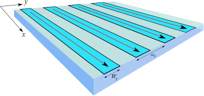
We assume that an array of narrow graphene nanoribbons lies on a substrate with the dielectric constant in the plane , Figure 1. The nanoribbons are infinite in the -direction and have the width in the -direction. The period of the structure in the -direction is . We assume that a sufficiently strong dc electric field is applied to the structure and a stationary charge current flows along the ribbons in the -direction. In addition, a space- and time-dependent electric field influences the system, so that the total external field acting on electrons in the ribbons amounts to
| (1) |
Our goal is to calculate the linear response of the system to the ac electric field not assuming that the dc field is weak, i.e. the response of the system to the dc field is aimed to be taken into account non-perturbatively.
The energy spectrum of electrons in two-dimensional graphene is described by the known linear dispersion relation where cm/s is the Fermi velocity in grapheneCastro Neto et al. (2009), is the quasi-momentum, and the upper (lower) sign corresponds to the electron (hole) energy band. We assume that in a single nanoribbon with the width the momentum is quantized, so that the quasi-one-dimensional spectrum of electrons and holes has the form
| (2) |
where is the subband index () and
| (3) |
is the half of the band gap in the ribbon Yang et al. (2007).
If the dc and ac electric fields (1) are applied to the system of nanoribbons, its response can be described by quasi-classical Boltzmann equations written for the distribution functions of electrons and holes in all occupied subbands (we consider the low-frequency range, , when the interband optical transitions can be neglected). Our previous studies Mikhailov (1998, 2013); Moskalenko and Mikhailov (2014) showed that, in order to realize the negative conductivity of the system, the density of electrons should be sufficiently low (this conclusion is also confirmed by the present work). Almost everywhere in this paper we will therefore assume that the chemical potential lies in the upper half of the forbidden band, , and the temperature is low, . Under these conditions one may consider only the response of electrons of the lowest () conduction () subband and ignore the inter-subband scattering. Then the Boltzmann equation for electrons of the subband assumes the form (we omit the indexes )
| (4) |
where is the elementary charge, the dc field is assumed to be negative, , , and is the scattering integral. The latter describes the scattering of graphene electrons by impurities, phonons, grain boundaries, etc., and is, in general, a complicated functional of the distribution function . Since we aim to get a non-perturbative (in ) solution of the problem we will assume a simple relaxation time () model for the scattering integral,
| (5) |
This approximation for is sufficiently reasonable and allows us to get an exact analytical solution of the response problem at a strong driving dc electric field. The function in Eq. (5) is the Fermi distribution function describing the local equilibrium Mermin (1970); Kragler and Thomas (1980)
| (6) |
it differs from the global equilibrium distribution
| (7) |
by the space and time dependence of the local chemical potential . The local chemical potential is determined from the particle conservation condition Mermin (1970); Kragler and Thomas (1980)
| (8) |
the global chemical potential is denoted as .
II.2 Parameters
In this paper we utilize the value of , Eq. (3), as the energy scale and measure the frequency, wave vector, scattering rate, chemical potential, temperature and the electric field in the following dimensionless units
| (9) |
where is the mean free path and is the scattering rate. Consider an illustrative numerical example. Assume that the ribbon width is nm. Then the value of the energy scale is meV. This is equivalent to K and THz. The temperature parameter thus corresponds to K, and the dimensionless frequency to about THz. The spatial periodicity of the external ac electric field can be created by placing a grating (with the period in the -direction) in the vicinity of the nanoribbon array. Then and the dimensionless wave-vector parameter can vary from values small as compared to unity up to and above. The value of corresponds to the grating period nm.
The scattering parameter depends on the sample quality. With nm and the mean free path about 1.3 m, the factor constitutes about . The field parameter reaches 1 at V/cm in the samples with the indicated value of the mean free path. At V/cm mV/m we have .
II.3 Equilibrium density
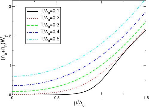
Now we consider the equilibrium linear density of charge carriers (electrons and holes ) as a function of the chemical potential at different temperatures. The result reads (here, in Section II.3 only, we take into account all electron and hole subbands)
| (10) |
where are the spin and valley degeneracies, and
| (11) |
The -dependence of the total dimensionless charge density is shown in Figure 2. At and the parameter ; under these conditions the main contribution to the density is given by electrons of the lowest subband. If nm, the linear charge density is about /cm. If the aspect ratio of the nanoribbon array is about the two-dimensional (2D) average charge carrier density is
| (12) |
It will be seen below that the amplification of the waves in the current driven system of graphene nanoribbons can be achieved at low electron densities. The number (12) gives a typical scale of the charge carrier density needed for the realization of the amplification.
II.4 Solution of the Boltzmann equation
| (13) |
Substituting
| (14) |
and
| (15) |
into Eq. (13), where , we get the linearized (in ) version of the Boltzmann equation
| (16) |
From the charge-density conservation condition (8) we get
| (17) |
The solution of the linearized Boltzmann equation (16) is searched for in the form . Then we obtain
| (18) |
The second term in the left-hand side contains an unknown constant . To find it we perform summation over in both sides of Eq. (18) and get
| (19) |
The solution of the Boltzmann equation then assumes the form
| (20) |
II.5 Current density
Calculating the current according to the standard formula
| (21) |
where is the ribbon length in the -direction, we obtain
| (22) |
Here we have defined the integrals
| (23) |
After some transformations they can be presented in the following form
| (24) |
with the dimensionless integrals
| (25) |
can be evaluated numerically as functions of all their dimensionless arguments.
II.6 Dynamic conductivity
The current in Eq. (21) is a one-dimensional (1D) current flowing in a single nanoribbon. The corresponding 1D dynamic conductivity is . In an array of nanoribbons it is reasonable to determine the 2D conductivity as an average current density flowing in all nanoribbons divided by the electric field. It is related to the 1D conductivity as
| (26) |
Then we get for :
| (27) |
where
| (28) |
If, instead of one, the system consists of several () parallel graphene nanoribbon layers, the right hand side of Eq. (27) should be multiplied by .
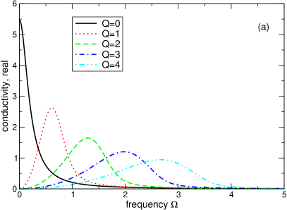
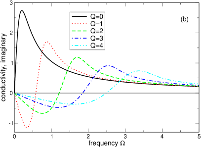
Figure 3 shows the frequency dependence of the dimensionless conductivity from Eq. (27) at different wave vectors. The real (Fig. 3(a)) and imaginary (Fig. 3(b)) parts of the conductivity are even and odd functions of , respectively. At Eq. (27) is reduced to the Drude formula (black solid curves in Figure 3). At a larger the maximum is shifted to larger values of and becomes broader. The maxima are located at due to the single particle absorption caused by electrons moving with the velocity smaller than . The imaginary part of the conductivity, Figure 3(b), is connected to the real part by the Kramers-Kronig relations.
II.7 Dielectric function
If the 2D layer with the conductivity lies on the dielectric substrate with the dielectric constant , the effective dielectric function of such a system can be determined as Stern (1967)
| (29) |
where is the effective dielectric constant of the surrounding medium. Substituting the expression for the conductivity (27) we get
| (30) |
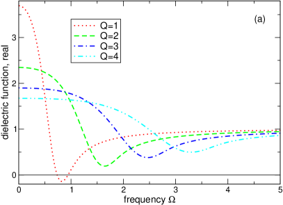
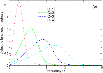
The real and imaginary parts of the dielectric function (30) are shown in Figure 4.
II.8 Absorption
If the potential of the external electric field is , the potential of the total electric field acting on graphene electrons is , and the induced linear-response current reads
| (31) |
The time-averaged Joule heat is then given by . If we assume that the time-averaged magnitude of the Poynting vector of the incident wave is , the absorption coefficient can be found as
| (32) |
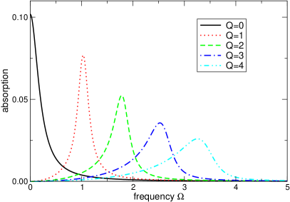
The absorption spectrum of an array of graphene nanoribbons is shown in Figure 5. The maxima of the absorption coefficient are shifted with respect to those of Re to higher frequencies, and the linewidths are a bit narrower. Notice that, under the chosen conditions (, ) and at the real part of the dielectric function , Figure 4(a), does not vanish at any frequency, i.e. the 2D plasmons whose spectrum satisfies the equation Re , do not exist. The absorption maxima in Figure 5 at thus have the single-particle origin. At smaller these maxima correspond to the collective (2D plasmon) resonance.
III DC response of a current driven system
Now we consider the case when a strong dc electric field is applied to the system but the amplitude of the ac field is zero, . We calculate the stationary non-equilibrium distribution function which is formed under the action of the dc field whereas the scattering processes are described within the -approximation (5).
III.1 Stationary distribution function
Under the action of the uniform and time-independent electric field the Boltzmann equation for the stationary distribution function reads (we assume and ):
| (33) |
It is solved by the separation of variables method; the solution can be written in the following dimensionless form
| (34) |
where we have used the boundary condition at and introduced the normalized momentum . The function (34) satisfies the condition
| (35) |
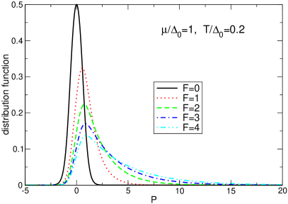
and is shown in Figure 6. At and electrons move in the positive -direction. One sees that the stationary distribution function is strongly asymmetric and substantially differs from the equilibrium distribution function already at .
III.2 Stationary dc current and average drift velocity
Having obtained the stationary distribution function we now calculate the dc current density (21). It can be reduced to the dimensionless form
| (36) |
where
| (37) |
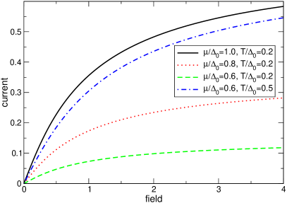
The dc-field dependence of the current for several values of the chemical potential and temperature is illustrated in Figure 7. The current-voltage characteristics is linear only at . At larger values of one sees substantial deviations from the Ohm’s law.
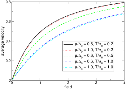
The average drift velocity of electrons in the first electron subband,
| (38) |
is shown in Figure 8; here
| (39) |
is the dimensionless velocity of electrons in the first electron subband. Notice that weakly depends on the chemical potential but is sensitive to a change of the temperature.
The - characteristics similar to the one shown in Figure 7 have been experimentally observed in graphene, see, e.g., Fig. 2b in Ref. Barreiro et al. (2009). The average drift velocity which was achieved in that paper (at much higher electron density and temperature than we assume here) was about which confirms the feasibility of our model.
IV AC response of a current driven system
IV.1 Dynamic distribution function in a driven system
Now we consider the system response to the ac electric field in the presence of the strong dc driving field . It is described by the Boltzmann equation (4)–(5). We search for a solution in the form
| (40) |
where is the stationary distribution function found in Section III, Eq. (33), and is the correction proportional to the perturbation . Linearizing the Boltzmann equation we get the following equation for :
| (41) |
Since the perturbation is proportional to , we search for a solution with the same spatio-temporal form and obtain the integro-differential equation for :
| (42) |
Its general solution reads:
| (43) |
where
| (44) |
is, again, an unknown constant proportional to , cf. Eq. (18). It can be found by taking a sum over in Eq. (43):
| (45) |
The formulas (43) and (45) give the closed-form analytical expression for the electron distribution function in a direct current driven system of graphene nanoribbons.
IV.2 Current density, field-dependent conductivity and absorption coefficient: Analytic formulas
In order to calculate the current density in a dc-driven graphene nanoribbon we substitute the distribution function (43), (45) into the definition (21). The dc-field dependent 1D conductivity of a single nanoribbon is then given by the relation , and the effective 2D conductivity of an array of nanoribbons is determined by Eq. (26). Introducing dimensionless variables , , and (9) we get the following expression for the 2D conductivity:
| (46) |
where the formula is written for parallel graphene nanoribbon layers and the dimensionless function is determined by the formula
| (47) |
Here we have defined the following functions:
| (48) |
| (49) |
| (50) |
where
| (51) |
Equations (47) – (51) determine the current-driven nonlocal frequency-dependent conductivity of an array of graphene nanoribbons as a function of the frequency , wave-vector , scattering rate , chemical potential , temperature and the driving dc electric field . Without the driving field, , the function is reduced to ,
| (52) |
defined in Eq. (28).
The effective dielectric function is introduced like in Section II.7; it is now related to the function :
| (53) |
The formula for the absorption coefficient in the current driven system of graphene nanoribbons is given by Eq. (32), in which the function and should be taken from Eqs. (46) and (53) respectively.
The formulas (46), (53) and (32) determine the electrodynamic response of the system of graphene nanoribbons driven by a strong dc current. In order to proceed further and plot the corresponding figures we have to numerically calculate the integrals , and in Eqs. (48) – (50). The integral (50) can be easily calculated since the integrand of this function is a localized function of . The integrals and, especially, , require a careful treatment since they are, in fact, a double () and triple () integrals with strongly oscillating (due to the exponential function ) integrands. The method utilized for numerical evaluation of such integrals is briefly described in Appendix A.
IV.3 Dynamic conductivity and absorption: Results
Using the numerical integration technique described in Appendix A we now calculate the dynamic conductivity and the absorption coefficient of a current driven system of graphene nanoribbons at different values of the input parameters. Figure 9 shows typical spectra of the real and imaginary parts of the dimensionless conductivity (47). The parameters , and are the same as in Figure 3, the wavevector . In Figure 9 we show the spectra both at negative and positive frequencies. Since we have searched for a solution in the form , the positive (negative) frequencies correspond to the wave running in the positive (negative) direction of the -axis. Since the drift velocity of electrons is positive at , at positive frequencies the wave and electrons move in the same direction, while at negative frequencies they move in the opposite directions.
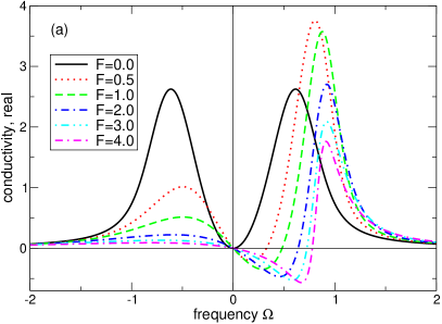
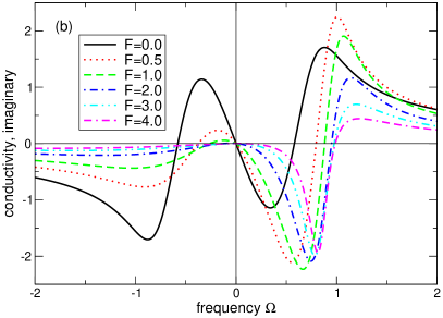
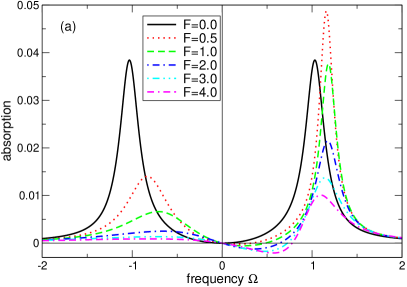
As seen from Figure 9, at (black solid curves) the real (imaginary) part of the dynamic conductivity is an even (odd) function of the frequency . The real part has two symmetric maxima at which means that the waves running in opposite directions are absorbed equally and that the maximum absorption is the case for the wave running with the phase velocity . Similar features can be seen in the absorption spectra, Figure 10, but the maxima are the case at and the absorption lines are a bit narrower, which is due to the influence of the dielectric function (53) in the denominator of Eq. (32).
When the dc field is switched on, , the position and the linewidth of the conductivity and absorption resonances are modified. If (the wave and the electron beam propagate in opposite directions) the resonance is shifted to the lower frequencies and gets broader. At positive frequencies (the wave and the electron beam propagate in the same direction) the resonance is first shifted to a larger and gets slightly narrower (at ); at stronger dc fields (at ) it broadens again. The most interesting feature of the conductivity and absorption spectra is the appearance of a finite frequency interval where the real part of the conductivity and of the absorption coefficient becomes negative, see details in Figure 10(b). The negative absorption means that the wave is amplified taking the energy from the electron beam. This effect is the case only if the wave and electrons run in the same direction () and if the frequency satisfies a critical condition , where depends on the driving dc electric field and other system parameters. Another interesting point characterizes the position of the maximum negative absorption, see Figure 10(b).
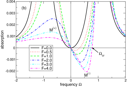
At and the critical frequency is about 0.78 and the maximum negative absorption is about % at . At the physical parameters outlined in Section II.2 the values of and correspond to 480 and 360 GHz respectively. The amplification coefficient 0.2% does not seem to be small if to remember that we are dealing with only a monolayer of atoms with the very low areal density of electrons cm-2 (at parameters from Section II.2, see the estimate in Eq. (12)).
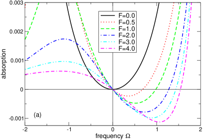
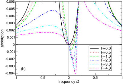
If the wavevector is two times larger, Figure 11(a), the critical frequency increases up to (corresponds to THz) but the maximum amplification (negative absorption) decreases, %. If the wavevector gets smaller, see Figure 11(b) for , the value of % increases, but the critical frequency (corresponds to GHz) decreases.
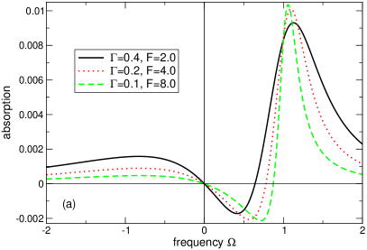
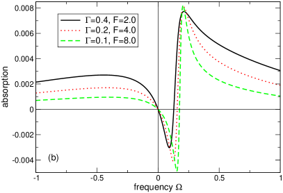
Figure 12 illustrates the influence of the scattering rate on the absorption spectra. Here we show the spectra for the curves from Figure 10(b) () and 11(b) () together with two other curves corresponding to two times smaller and two times larger values of the scattering rate . We notice that the scattering rate enters two dimensionless quantities and , see Eq. (9). Therefore reducing by a factor of two leads to the reduction of by the factor of two and to the increase of by the same factor. One sees that increasing reduces both the negative absorption region ( decreases) and the maximum amplification value .
For numerical parameters used in this paper (see Section II.2) the value of corresponds to the mean free path m. The -values of this (and larger) scale have been observed in graphene sandwiched between two h-BN crystals, e.g. Ref. Mayorov et al. (2011). It should be noticed that the scattering rate should be considered as a phenomenological parameter which may depend, for example, on the electron density, temperature or dc electric field. For example, at electrons may get enough energy to emit optical phonons or to be scattered to higher electron subbands. The first process is however unlikely since the typical energy of the optical phonons in the considered systems ( meV) is times larger than the energy scale in our problem ( meV, Section II.2). The scattering to the higher subbands is more likely but we believe that such a scattering should not dramatically influence our results: the probability of the elastic (e.g. impurity) scattering from to states is much higher than to the states (due to the smaller momentum transfer) but the processes lead to small current changes since after the scattering electrons continue to move in the same direction (here the first number in the ket states denotes the subband index, , and the states are the states with the same energy but different, positive and negative, momentum).
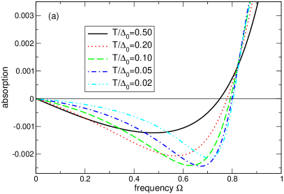
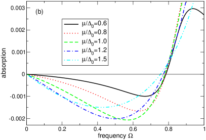
The influence of the temperature and the chemical potential on the maximum value of the negative absorption is illustrated in Figure 13. One sees that the critical point slightly grows with decreasing temperature and the chemical potential (i.e. with decreasing the electron density). The maximum amplification value has an optimum as a function of both and . At the parameters of Figure 13 this optimum lies at approximately % and is achieved at and .
The rather small value of the parameter corresponds, in the chosen numerical example with nm and K (Section II.1), to cryogenic temperatures K. The operation temperature of devices based on the discussed effect (e.g. of the Smith-Purcell-type emitter of terahertz radiation, see discussion in Section V) can be increased if the nanoribbons could be made substantially narrower. For example, at nm the gap corresponds to K, so that the room-temperature operation becomes feasible.
Analyzing all so far presented results one can notice that the critical frequency , which restricts the negative absorption region from above, is related to the average velocity of electrons in our system of graphene nanoribbons, Figure 8. Comparing the absorption plots with Figure 8 one can observe that . The amplification of the electromagnetic wave is thus the case when the drift velocity of electrons exceeds the phase velocity of the wave,
| (54) |
Under this condition the electron flow transmits its energy to the wave and amplifies it; under the opposite condition the wave transmits its energy to the electron system which leads to an additional damping of the wave and to the electron drag effect (not studied here). Notice that being written in the form (54) the amplification condition does not depend on details of the considered structure and its parameters and has therefore a larger range of applicability than the initial model.
The studied phenomenon is closely related to the acoustoelectric effect, in which the running electric-field excitation is created by a surface acoustic wave propagating in a piezoelectric material underlying the 2D electron system. The acoustoelectric interaction has been widely used and studied in semiconductor structures with the 2D electron gas, see e.g. Wixforth et al. (1986); Falko et al. (1993), as well as recently in graphene and other (e.g. MoS2) two-dimensional crystals Bandhu et al. (2013); Bandhu and Nash (2014); Preciado et al. (2015). It should be noticed however that the discussed effect in graphene offers substantially more opportunities as compared to semiconductors: while in semiconductors the drift velocity cannot be made very high so that one can only study the interaction of the drifting electrons with the (relatively slow) acoustic waves ( cm/s), in graphene the drift velocity can approach the Fermi velocity cm/s, which makes it possible to study the interaction of drifting electrons with faster electromagnetic excitations, e.g. with 2D plasma waves. This work thus also contributes to the theory of graphene-based voltage-tunable terahertz emitter proposed and discussed in Refs. Mikhailov (2013); Moskalenko and Mikhailov (2014).
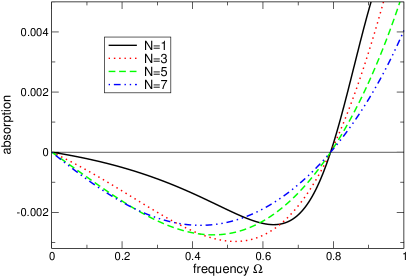
Finally, we would like to discuss the following point. The absolute value of the amplification factor was found to be rather small, below %, which is mainly due to the low density of electrons in a system which has only one (structured) monolayer of carbon atoms. Naturally the question arises, whether the factor can be increased by forming a many-layered system of parallel graphene-nanoribbon arrays. Figure 14 answers this question. It shows the absorption spectra of an array of the current-driven graphene nanoribbons for different numbers of layers . At the maximum negative absorption is about %. When increases, the absolute value of first grows with , indeed, but at it reaches a maximum (%) and then decreases again. Such a behavior becomes clear from Eqs. (32), (46) and (53): The number of layers enters both the nominator () and the denominator (which grows as at ). The suppression of the factor at large is thus due to the dielectric function (53). This suppression is unavoidable but may depend on (and be controlled by) the specific dielectric environment. By a special design of the environment one can probably increase the absolute value of the amplification factor but this problem is not considered in the present work.
V Conclusions
To summarize, we have studied the wave-vector, frequency, dc electric field, scattering rate, electron density, temperature and the number-of-layers dependence of the dynamic conductivity, dielectric function and the absorption coefficient in a direct current driven array of graphene nanoribbons. The influence of the dc electric field is taken into account non-perturbatively, the influence of the ac field – within the linear response theory, the scattering processes – within the simple relaxation time approximation. We have shown that, at frequencies satisfying the condition (54), the propagating electromagnetic wave can be amplified at the expense of the energy of the direct current source. We have analyzed the optimal conditions for the wave amplification depending on all system parameters.
We have assumed that the external electric field acting on the system is given by the formula (1) but did not discuss how the ac part of this field is created. This can be done by different means. For example, the running electric-field wave can be produced by the surface acoustic waves propagating along the surface of a piezoelectric material covered by graphene Bandhu et al. (2013); Bandhu and Nash (2014), a semiconductor 2D crystal Preciado et al. (2015), or by a graphene nanostructure as considered in this paper. In this case the phase velocity of the wave is about cm/s () and the required drift velocity and the dc electric field are very low (, ), see Figure 8.
Another opportunity to create the running electric-field wave (1) is to irradiate the graphene-nanoribbon array with an adjacent grating structure by electromagnetic radiationMikhailov (2013). The grating transforms the incident wave to the electromagnetic excitation running along the 2D layer with the phase velocity (with being the speed of light), thus realizing a Smith-Purcell-type emitter of radiation Smith and Purcell (1953). In this case the phase velocity of the wave can be comparable with the Fermi velocity of electrons in graphene, cm/s, which make it feasible to extend the operation frequency range up to terahertz. Attempts to realize such emitters of terahertz radiation have been made in the past on the basis of semiconductor structures Tsui et al. (1980); Hirakawa et al. (1995), for reviews see, e.g. Mikhailov (1998); Otsuji et al. (2011, 2012). Recently it has been proposed to use graphene for this purpose Mikhailov (2013); Moskalenko and Mikhailov (2014). This work thus contributes to the realization of graphene-based voltage-tunable emitters of sub-terahertz and terahertz radiation.
We thank Geoffrey Nash, Jérôme Faist, Isaac Luxmoore, Federico Valmorra, Janine Keller and Hua Qin for numerous discussions of issues related to the experimental realization of the graphene-based terahertz emitters. The work has received funding from the European Union under the FET-open grant GOSFEL (grant agreement No. 296391) and the European Union’s Horizon 2020 research and innovation programme Graphene Flagship under grant agreement No. 696656.
Appendix A Method of calculating the integrals
We aim to develop an efficient method of a numerical evaluation of the following integrals
| (55) |
where , is the exponential function (51) and is the dimensionless velocity (39). The functions and in Eqs. (48)–(49) are special cases of (55) if
| (56) |
and
| (57) |
respectively; here
| (58) |
is the equilibrium Fermi distribution function expressed in the dimensionless variables. A direct numerical integration in Eq. (55) runs into problems: the function strongly oscillates, which leads to a very long integration time as well as to error messages like “the required accuracy was not achieved”. To solve this problem we had to find a more elegant way to calculate the integral (55).
First, let us change the order of integration over and and make the substitution , . This gives
| (59) |
where the new function is defined as
| (60) |
The function in Eq. (59) is smooth and localized, therefore the problem is only in the functions , Eq. (60). The integrand in (60) is a strongly oscillating function of . But, considering it as a function of a complex variable ,
| (61) |
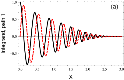
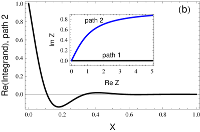
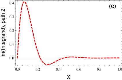
(here and ), we see that it is an analytical function in the whole complex plane . Therefore we can choose another integration path from the point to the complex infinity without changing the value of the integral. Choosing the integration path so that the integrand oscillations are substantially suppressed we can calculate the integrals much faster and without error messages.
Figure 15 illustrates this approach. In Figure 15(a) we show the real and imaginary parts of the integrand (61) if varies along the integration path 1 (the real axis ); the path 1 is shown by the black line in the inset to Figure 15(b). One sees that both the real and imaginary parts weakly decay and strongly oscillate when increases. In Figures 15(b,c) we choose another path, , , shown by the blue curve in the inset to Figure 15(b). The real and imaginary parts of the integrand (61) (shown in Figures 15(b) and (c) respectively) tend to zero much faster and without oscillations. The path 2 may depend on parameters , , and but a suitable path can always be found.
References
- Mikhailov (2007) S. A. Mikhailov, Europhys. Lett. 79, 27002 (2007).
- Dragoman et al. (2010) M. Dragoman, D. Neculoiu, G. Deligeorgis, G. Konstantinidis, D. Dragoman, A. Cismaru, A. A. Muller, and R. Plana, Appl. Phys. Lett. 97, 093101 (2010).
- Hotopan et al. (2011) G. Hotopan, S. Ver Hoeye, C. Vazquez, R. Camblor, M. Fernández, F. Las Heras, P. Álvarez, and R. Menéndez, Progress In Electromagnetic Research 118, 57 (2011).
- Hendry et al. (2010) E. Hendry, P. J. Hale, J. J. Moger, A. K. Savchenko, and S. A. Mikhailov, Phys. Rev. Lett. 105, 097401 (2010).
- Wu et al. (2011) R. Wu, Y. Zhang, S. Yan, F. Bian, W. Wang, X. Bai, X. Lu, J. Zhao, and E. Wang, Nano Lett. 11, 5159 (2011).
- Gu et al. (2012) T. Gu, N. Petrone, J. F. McMillan, A. van der Zande, M. Yu, G. Q. Lo, D. L. Kwong, J. Hone, and C. W. Wong, Nature Photonics 6, 554 (2012).
- Zhang et al. (2012) H. Zhang, S. Virally, Q. Bao, L. K. Ping, S. Massar, N. Godbout, and P. Kockaert, Optics Letters 37, 1856 (2012).
- Bykov et al. (2012) A. Y. Bykov, T. V. Murzina, M. G. Rybin, and E. D. Obraztsova, Phys. Rev. B 85, 121413(R) (2012).
- Kumar et al. (2013) N. Kumar, J. Kumar, C. Gerstenkorn, R. Wang, H.-Y. Chiu, A. L. Smirl, and H. Zhao, Phys. Rev. B 87, 121406(R) (2013).
- Hong et al. (2013) S.-Y. Hong, J. I. Dadap, N. Petrone, P.-C. Yeh, J. Hone, and R. M. Osgood, Jr., Phys. Rev. X 3, 021014 (2013).
- An et al. (2014) Y. Q. An, J. E. Rowe, D. B. Dougherty, J. U. Lee, and A. C. Diebold, Phys. Rev. B 89, 115310 (2014).
- Mikhailov (2011) S. A. Mikhailov, Phys. Rev. B 84, 045432 (2011).
- Yao and Belyanin (2013) X. H. Yao and A. Belyanin, J. Phys. Condens. Matter 25, 054203 (2013).
- Cheng et al. (2014a) J. L. Cheng, N. Vermeulen, and J. E. Sipe, New J. Phys. 16, 053014 (2014a).
- Cheng et al. (2014b) J. L. Cheng, N. Vermeulen, and J. E. Sipe, Optics Express 22, 15868 (2014b).
- Peres et al. (2014) N. M. R. Peres, Y. V. Bludov, J. E. Santos, A.-P. Jauho, and M. I. Vasilevskiy, Phys. Rev. B 90, 125425 (2014).
- Smirnova et al. (2014) D. A. Smirnova, I. V. Shadrivov, A. E. Miroshnichenko, A. I. Smirnov, and Y. S. Kivshar, Phys. Rev. B 90, 035412 (2014).
- Yao et al. (2014) X. Yao, M. Tokman, and A. Belyanin, Phys. Rev. Lett. 112, 055501 (2014).
- Cox and de Abajo (2014) J. D. Cox and F. J. G. de Abajo, Nat. Commun. 5, 5725 (2014).
- Cheng et al. (2015) J. L. Cheng, N. Vermeulen, and J. E. Sipe, Phys. Rev. B 91, 235320 (2015).
- Cheng et al. (2016) J. L. Cheng, N. Vermeulen, and J. E. Sipe, Phys. Rev. B 93, 039904(E) (2016).
- Sabbaghi et al. (2015) M. Sabbaghi, H.-W. Lee, T. Stauber, and K. S. Kim, Phys. Rev. B 92, 195429 (2015).
- Savostianova and Mikhailov (2015) N. A. Savostianova and S. A. Mikhailov, Appl. Phys. Lett. 107, 181104 (2015).
- Cox and de Abajo (2015) J. D. Cox and F. J. G. de Abajo, ACS Photonics 2, 306 (2015).
- Mikhailov (2016) S. A. Mikhailov, Phys. Rev. B 93, 085403 (2016).
- Cox et al. (2016) J. D. Cox, I. Silviero, and F. J. G. de Abajo, ACS NANO 10, 1995 (2016).
- Marini et al. (2016) A. Marini, J. D. Cox, and F. J. G. de Abajo, arXiv:1605.06499 (2016).
- Mikhailov (2013) S. A. Mikhailov, Phys. Rev. B 87, 115405 (2013).
- Moskalenko and Mikhailov (2014) A. S. Moskalenko and S. A. Mikhailov, J. Appl. Phys. 115, 203110 (2014).
- Bandhu et al. (2013) L. Bandhu, L. M. Lawton, and G. R. Nash, Appl. Phys. Lett. 103, 133101 (2013).
- Bandhu and Nash (2014) L. Bandhu and G. R. Nash, Appl. Phys. Lett. 105, 263106 (2014).
- Preciado et al. (2015) E. Preciado, F. J. R. Schulein, A. E. Nguyen, D. Barroso, M. Isarraraz, G. von Son, I.-H. Lu, W. Michailow, B. Moller, V. Klee, et al., Nat. Commun. 6, 8593 (2015).
- Sablikov and Chenskii (1996) V. A. Sablikov and E. V. Chenskii, JETP 82, 900 (1996).
- Kim et al. (2004) K. W. Kim, V. V. Korotyeyev, V. A. Kochelap, A. A. Klimov, and D. L. Woolard, J. Appl. Phys. 96, 6488 (2004).
- Castro Neto et al. (2009) A. H. Castro Neto, F. Guinea, N. M. R. Peres, K. S. Novoselov, and A. K. Geim, Rev. Mod. Phys. 81, 109 (2009).
- Yang et al. (2007) L. Yang, C.-H. Park, Y.-W. Son, M. L. Cohen, and S. G. Louie, Phys. Rev. Lett. 99, 186801 (2007).
- Mikhailov (1998) S. A. Mikhailov, Phys. Rev. B 58, 1517 (1998).
- Mermin (1970) N. D. Mermin, Phys. Rev. B 1, 2362 (1970).
- Kragler and Thomas (1980) R. Kragler and H. Thomas, Z. Phys. B 39, 99 (1980).
- Stern (1967) F. Stern, Phys. Rev. Lett. 18, 546 (1967).
- Barreiro et al. (2009) A. Barreiro, M. Lazzeri, J. Moser, F. Mauri, and A. Bachtold, Phys. Rev. Lett. 103, 076601 (2009).
- Mayorov et al. (2011) A. S. Mayorov, R. V. Gorbachev, S. V. Morozov, L. Britnell, R. Jalil, L. A. Ponomarenko, P. Blake, K. S. Novoselov, K. Watanabe, T. Taniguchi, et al., Nano Lett. 11, 2398 (2011).
- Wixforth et al. (1986) A. Wixforth, J. P. Kotthaus, and G. Weimann, Phys. Rev. Lett. 56, 2104 (1986).
- Falko et al. (1993) V. I. Falko, S. V. Meshkov, and S. V. Iordanskii, Phys. Rev. B 47, 9910 (1993).
- Smith and Purcell (1953) S. J. Smith and E. M. Purcell, Phys. Rev. 92, 1069 (1953).
- Tsui et al. (1980) D. C. Tsui, E. Gornik, and R. A. Logan, Solid State Commun. 35, 875 (1980).
- Hirakawa et al. (1995) K. Hirakawa, K. Yamanaka, M. Grayson, and D. C. Tsui, Appl. Phys. Lett. 67, 2326 (1995).
- Otsuji et al. (2011) T. Otsuji, T. Watanabe, M. A. E., K. H., T. Komori, A. Satou, T. Suemitsu, M. Suemitsu, E. Sano, W. Knap, et al., J. Infrared Milli. Terahz. Waves 32, 629 (2011).
- Otsuji et al. (2012) T. Otsuji, S. A. B. Tombet, A. Satou, H. Fukidome, M. Suemitsu, E. Sano, V. Popov, M. Ryzhii, and V. Ryzhii, J. Phys. D: Appl. Phys. 45, 303001 (2012).